T33 Module Datasheet
Last Updated on : 2023-06-12 09:43:04download
T33 is a fully integrated single chip that integrates all peripheral devices. The chip integrates complete hardware and software resources required by Wi-Fi and Bluetooth applications, can support AP and STA dual-role connections, and support Bluetooth connections at the same time.
Overview
A 32-bit MCU with a running speed of up to 120 MHz and a built-in 256 KB RAM can enable the chip to support multi-cloud connections, and the MCU’s special instructions for signal processing can effectively implement audio encoding and decoding.
T33 integrates crystals, RF matching circuits and all peripheral devices, and has rich peripherals, such as PWM, I2C, UART, SPI, SDIO, USB and IrDA Up to six 32-bit PWM outputs, making the chip very suitable for high-quality LED control.
Features
- Embedded low-power 32-bit CPU, which can also function as an application processor
- The maximum clock rate: 120 MHz
- Working voltage: 3.3 ± 0.3V
- Peripherals: 6 PWMs, 2 I2Cs, 2 UARTs, 1 SPI, and 1 USB
- Wi-Fi connectivity
- 802.11 b/g/n
- Channels 1 to 14 at 2.4 Ghz
- Support WEP,WPA/WPA2,WPA/WPA2 PSK (AES) security modes
- Up to +17 dBm output power in 802.11b mode
- Support STA/AP/STA+AP working mode
- Support SmartConfig and AP network configuration manners for Android and iOS devices
- Working temperature: -40 to 105℃
- Bluetooth connectivity
- Up to 20 dBm transmit power in bluetooth mode
- Bluetooth coexistence interface
Applications
- Intelligent building
- Smart household and home appliances
- Smart socket and light
- Industrial wireless control
- Baby monitor
- Network camera
- Intelligent bus
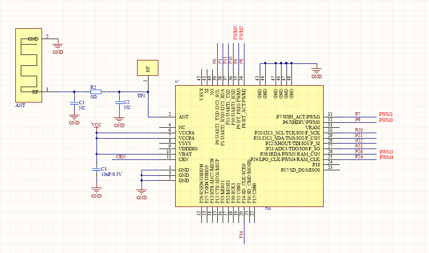
Module interfaces
Dimensions and footprint
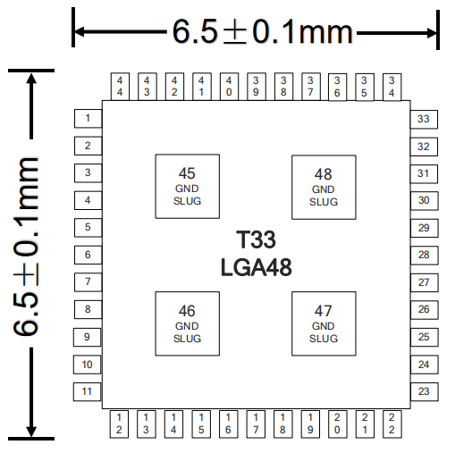
T33 is packaged in the form of LGA 6.5x6.5 48-pin.
The T33 dimensions are 6.5±0.1 mm (W)×6.5±0.1 mm (L) ×0.98±0.1 mm (H).
The dimensions of T33 are as follows:
Pin definition
| Pin number | Symbol | I/O type | Function |
|---|---|---|---|
| 1, 3, 5, 43, 44, 45, 46, 47 and 48 | GND | P | ground |
| 2 | ANT | I/O | External antenna with 2.4 GHz RF output/input |
| 4 | NC | / | No connection |
| 6 | VCCPA | P | RF PA power input, voltage is 3.0 to 3.6V, 3.3 V recommended |
| 7 | VCCPA | P | RF PA power input, voltage is 3.0 to 3.6V, 3.3 V recommended |
| 8 | VSYS | O | System power output, voltage is about 2.7 to 3.0 V, not connected by default |
| 9 | VDDDIG | O | Digital power output, voltage is around 1.2 V |
| 10 | VBAT | P | Chip main power input, voltage is 3.0 to 3.6V, 3.3 V recommended |
| 11 | CEN | I | Enable a chip, high effective |
| 12 | P28/RXEN/USBDN | I/O | Set high or USBDN during receiving of a universal IO interface or RF |
| 13 | P25/TXEN/USBDP | I/O | Set high or USBDN during transmission of a universal IO interface or RF |
| 14 | P13/RTS/ADC7/MICN | I/O | A universal IO interface, RTS of UART1, ADC or the input negative end of a microphone |
| 15 | P12/CTS/ADC6/MICP | I/O | A universal IO interface, CTS of UART1, ADC or the input positive end of a microphone |
| 16 | P33/MISO1 | I/O | A universal IO interface or MISO of SPI1 |
| 17 | P32/MOSI1 | I/O | A universal IO interface or MOSI of SPI1 |
| 18 | P30/SCK1 | I/O | A universal IO interface or SCK of SPI1 |
| 19 | P31/CSN1 | I/O | A universal IO interface or MISO of SPI1 |
| 20 | P14/SD_CLK/SCK0 | I/O | A universal IO interface, CLK of SD, or SCK of SPI0 |
| 21 | P16/SD_CMD/MOSI0 | I/O | A universal IO interface, CMD of SD, or MOSI of SPI0 |
| 22 | P15/CSN0 | I/O | A universal IO interface or CSN of SPI0 |
| 23 | P17/SD_D0/MISO0 | I/O | A universal IO interface, D0 of SD, MISO of SPI0 |
| 24 | P18 | I/O | A universal IO interface |
| 25 | P24/LPO_CLK/PWM4/RAM_CLK | I/O | A universal IO interface or low-power clock 32.768-K output or PWM 4 or CLK of an external RAM |
| 26 | P26/IRDA/PWM5/RAM_CSN | I/O | A universal IO interface, infrared, PWM5, CSN of an external RAM |
| 27 | P23/ADC3/TDO/IO0/F_SO | I/O | A universal IO interface, ADC, TDO of JTAG, IO0 of QSPI, data output during flash download |
| 28 | P22/XHOUT/TDI/IO1/F_SI | I/O | A universal IO interface, crystal frequency output, TDO of JTAG, IO1 of QSPI, or data input during flash download |
| 29 | P21/I2C1_SDA/TMS/IO2/F_CSN | I/O | A universal IO interface, SDA of I2C1, TMS of JTAG, IO2 of QSPI, or chip selection during flash download |
| 30 | P20/I2C1_SCL/TCK/IO3/F_SCK | I/O | A universal IO interface, SCL of I2C1, TCK of JTAG, IO3 of QSPI, or clock during flash download |
| 31 | VRAM | O | Supply power to external RAM 1.8 V, 2.5 V, or 3.3 V |
| 32 | P6/XHDIV/PWM0 | I/O | A universal IO interface, 1, 2, 4, and 8 frequency division output of crystal clock or PWM0 |
| 33 | P7/WIFI_ACT/PWM1 | I/O | A universal IO interface or WIFI_ACTIVE or PWM1 with WIFI coexistence |
| 34 | P8/BT_ACT/PWM2 | I/O | A universal IO interface, BT_ACTIVE coexisting with Wi-Fi or PWM 2 |
| 35 | P9/BT_PRIO/PWM3 | I/O | A universal IO interface, BT_PRIORITY coexisting with Wi-Fi or PWM 3 |
| 36 | P10/UART1_RXD | I/O | A universal IO interface or RXD of a serial interface UART 1 |
| 37 | P11/UART1_TXD | I/O | A universal IO interface or TXD of a serial interface UART 1 |
| 38 | P1/UART2_RXD/I2C2_SDA | I/O | A universal IO interface, RXD of a serial interface UART 2 or I2C2_SDA |
| 39 | P0/UART2_TXD/I2C2_SCL | I/O | A universal IO interface, TXD of a serial interface UART 2 or I2C2_SCL |
| 40 | XO | O | 26 MHz crystal output terminal, not connected by default |
| 41 | XI | I | 26 MHz crystal input terminal, not connected by default |
| 42 | VSYS | I | System power output voltage is about 2.7 to 3.0 V |
Note: P indicates power supply pins and I/O indicates input/output pins.
Electrical parameters
Absolute electrical parameters
| Parameter | Description | Minimum value | Maximum value | Unit |
|---|---|---|---|---|
| Ts | Storage temperature | -55 | 125 | ℃ |
| VBAT | Power supply voltage | -0.3 | 3.9 | V |
| ESD voltage (human body model) | TAMB-25℃ | -2 | 2 | KV |
| ESD voltage (machine model) | TAMB-25℃ | -200 | 200 | V |
Normal working conditions
| Parameter | Description | Minimum value | Typical value | Maximum value | Unit |
|---|---|---|---|---|---|
| Ta | Working temperature | -40 | - | 105 | ℃ |
| VBAT | Power supply voltage | 3.0 | 3.3 | 3.6 | V |
| VIL | IO low-level input | -0.3 | - | VCC*0.25 | V |
| VIH | IO high-level input | VCC*0.75 | - | VCC | V |
| VOL | IO low-level output | VSS | - | VSS+0.3 | V |
| VOH | IO high-level output | VCC-0.3 | - | VCC | V |
| Imax | IO drive current | - | 6 | 20 | mA |
RF power consumption
| Working status | Mode | Rate | Transmit power/Receive | Average value | Peak value (Typical value)) | Unit |
|---|---|---|---|---|---|---|
| Transmit | 11 b | 11 Mbps | +17 dBm | 295 | 304 | mA |
| Transmit | 11 g | 54 Mbps | +13.5 dBm | 257 | 306 | mA |
| Transmit | 11 n | MCS 7 | +13 dBm | 260 | 251 | mA |
| Receive | 11b | 11 Mbps | Constantly receive | 98 | 150 | mA |
| Receive | 11g | 54 Mbps | Constantly receive | 98 | 147 | mA |
| Receive | 11n | MCS 7 | Constantly receive | 98 | 147 | mA |
Working current
| Working mode | Working status, Ta = 25°C | Average value | Maximum value (Typical value) | Unit |
|---|---|---|---|---|
| Quick connection state (Bluetooth) | The module is in the fast network connection state and the Wi-Fi indicator always flashes | 88 | 196 | mA |
| Quick connection state (AP ) | The module is in the hotspot network configuration state and the Wi-Fi indicator flashes slowly | 95 | 240 | mA |
| Quick connection state (EZ) | The module is in the fast network connection state and the Wi-Fi indicator always flashes | 105 | 232 | mA |
| Connected | The module is connected to the network and the Wi-Fi indicator is always on | 55 | 192 | mA |
| Disconnected | The module is disconnected and the Wi-Fi indicator is dark | 41 | 200 | mA |
RF parameters
Basic RF features
| Parameter | Description |
|---|---|
| Working frequency | 2.412 to 2.484GHz |
| Wi-Fi standard | IEEE 802.11 b/g/n (channels 1 to 14) |
| Data transmission rate | 11b: 1, 2, 5.5, 11 (Mbps); 11g: 6, 9, 12, 18, 24, 36, 48, 54 (Mbps); 11n: HT20 MCS 0 to 7 |
| Antenna type | PCB antenna, FPC antenna or ceramic antenna |
Wi-Fi transmission performance
| Parameter | Minimum value | Typical value | Maximum value | Unit |
|---|---|---|---|---|
| Average RF output power, 802.11b CCK Mode 11M | - | 16 | - | dBm |
| Average RF output power, 802.11g OFDM Mode 54M | - | 14 | - | dBm |
| Average RF output power, 802.11n OFDM Mode MCS7 | - | 12 | - | dBm |
| Frequency error | -10 | - | 10 | ppm |
Wi-Fi reception performance
| Parameter | Minimum value | Typical value | Maximum value | Unit |
|---|---|---|---|---|
| PER<8%, RX sensitivity, 802.11b DSSS Mode 11M | - | -85 | - | dBm |
| PER<10%, RX sensitivity, 802.11g OFDM Mode 54M | - | -72 | - | dBm |
| PER<10%, RX sensitivity, 802.11n OFDM Mode MCS7 | - | -68 | - | dBm |
| PER<10%, RX sensitivity, Bluetooth 1M | - | -94 | - | dBm |
Bluetooth transmission performance
| Parameter | Minimum value | Typical value | Maximum value | Unit |
|---|---|---|---|---|
| Working frequency | 2402 | - | 2480 | MHz |
| Air rate | - | 1 | - | Mbps |
| TX power | -20 | 6 | 20 | dBm |
| Frequency error | -150 | - | 150 | KHz |
Bluetooth reception performance
| Parameter | Minimum value | Typical value | Maximum value | Unit |
|---|---|---|---|---|
| RX sensitivity | - | -93 | - | dBm |
| Maximum RF signal input | -10 | - | - | dBm |
| Intermodulation | - | - | -23 | dBm |
| Co-channel suppression ratio | - | 10 | - | dB |
Antenna
Antenna type
T33 can choose an antenna according to the actual space and environment.
Antenna interference reduction
To ensure optimal Wi-Fi performance when the Wi-Fi module uses an onboard PCB antenna, it is recommended that the antenna be at least 15 mm away from other metal parts.
To ensure antenna performance, the PCB should not be routed or clad with copper in the antenna area.
Packaging information and production instructions
Mechanical dimensions
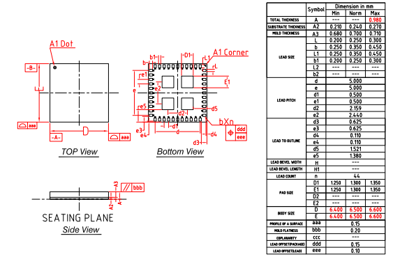
Schematic diagram
Production instructions
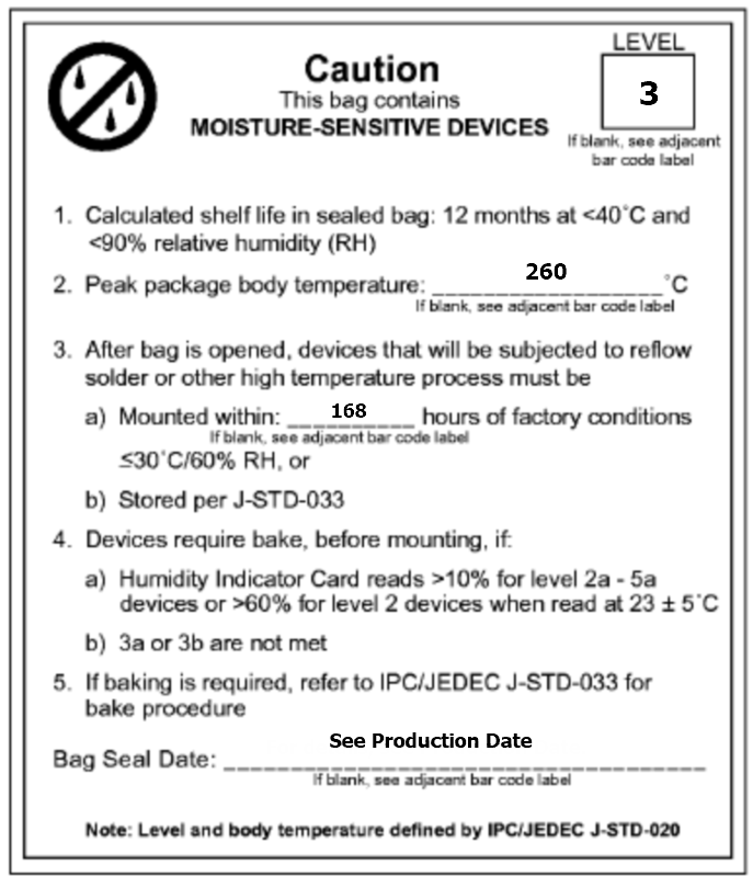
- The Tuya SMT module should be mounted by the SMT device. After being unpacked, it should be soldered within 24 hours. Otherwise, it should be put into the drying cupboard where the RH is not greater than 10%; or it needs to be packaged under vacuum again and the exposure time needs to be recorded (the total exposure time cannot exceed 168 hours).
- SMT devices:
- Mounter
- SPI
- Reflow soldering machine
- Thermal profiler
- Automated optical inspection (AOI) equipment
- Baking devices:
- Cabinet oven
- Anti-electrostatic and heat-resistant trays
- Anti-electrostatic and heat-resistant gloves
- SMT devices:
- Storage conditions for a delivered module:
-
The moisture-proof bag must be placed in an environment where the temperature is below 40°C and the relative humidity is lower than 90%.
-
The shelf life of a dry-packaged product is 12 months from the date when the product is packaged and sealed.
-
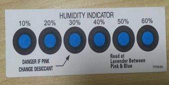
There is a humidity indicator card (HIC) in the packaging bag.
-
- The module needs to be baked in the following cases:
- The packaging bag is damaged before unpacking.
- There is no HIC in the packaging bag.
- After unpacking, circles of 10% and above on the HIC become pink.
- The total exposure time has lasted for over 168 hours since unpacking.
- More than 12 months have passed since the sealing of the bag.
- Baking settings:
- Temperature: 60°C and ≤ 5% RH for reel package and 125°C and ≤5% RH for tray package (please use the heat-resistant tray rather than plastic container)
- Time: 48 hours for reel package and 12 hours for tray package
- Alarm temperature: 65°C for reel package and 135°C for tray package
- Production-ready temperature after natural cooling: < 36°C
- Re-baking situation: If a module remains unused for over 168 hours after being baked, it needs to be baked again.
- If a batch of modules is not baked within 168 hours, do not use the reflow soldering to solder them. Because these modules are Level-3 moisture-sensitive devices, they are very likely to get damp when exposed beyond the allowable time. In this case, if they are soldered at high temperatures, it may result in device failure or poor soldering.
- In the whole production process, take electrostatic discharge (ESD) protective measures.
- To guarantee the passing rate, it is recommended that you use the SPI and AOI to monitor the quality of solder paste printing and mounting.
Recommended oven temperature curve
Set oven temperatures according to the following temperature curve of reflow soldering. The peak temperature is 245°C.
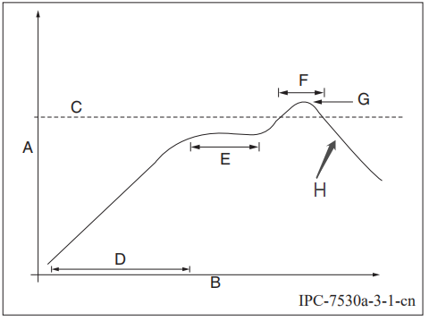
-
A: Temperature axis
-
B: Time axis
-
C: Liquidus temperature: 217 to 220°C
-
D: Ramp-up slope: 1 to 3°C/s
-
E: Duration of constant temperature: 60 to 120s; the range of constant temperature: 150 to 200°C
-
F: Duration above the liquidus: 50 to 70s
-
G: Peak temperature: 235 to 245°C
-
H: Ramp-down slope: 1 to 4°C/s
Note: The above curve is just an example of the solder paste SAC305. For more details about other solder pastes, please refer to Recommended oven temperature curve in the solder paste specifications.
Storage conditions
Storage conditions

MOQ and packing method
| Product number | Package | Packing method | MOQ |
|---|---|---|---|
| T33 | LGA48_6.5X6.5 | Tape reel | 3000 |
Is this page helpful?
YesFeedbackIs this page helpful?
YesFeedback


