NM1 Series Hardware Design
Last Updated on : 2023-03-07 07:59:29download
About this document
Applicability
These guidelines apply to NM1 series modules, including NM1, NM1-CT, and NM1-GL.
Purposes
These guidelines are intended to serve as the reference when you develop with NM1 series modules. It helps you get an overall understanding of the product specifications and assists in developing IoT products and applications.
This topic describes the hardware design guidelines in terms of features, specifications, reliability tests, test standards, development process, radio frequency (RF) metrics, and circuit designs.
Glossary
| Abbreviation | Spelled-out |
|---|---|
| ESD | Electrostatic discharge |
| USB | Universal serial bus |
| UART | Universal asynchronous receiver-transmitter |
| SIM | Subscriber identification module |
| SPI | Serial peripheral interface |
| I2C | Inter-integrated circuit |
| I/O | Input/Output |
| GPIO | General-purpose input/output |
| TBD | To be determined |
| RTC | Real time clock |
| ADC | Analog-to-digital converter |
Product overview
NM1 series is a family of compact, high-performance, and low-consumption NB-IoT modules. It features:
- Conforming to the NB-IoT radio protocols in 3GPP Release 13
- Frequency bands:
- NM1: B1/B3/B5/B8/B20
- NM1-CT: B5/B8
- NM1-GL: B1/B2/B3/B4/B5/B8/B12/B13/B14/B17/B18/B19/B20/B25/B26/B28/B66/B70/B85
- Support for both power saving mode (PSM) and extended discontinuous reception (eDRX)
- Abundant external interfaces including SIM card (1.8V), USB 1.1, UART, SPI, I2C, and GPIO
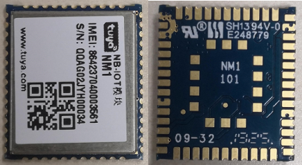
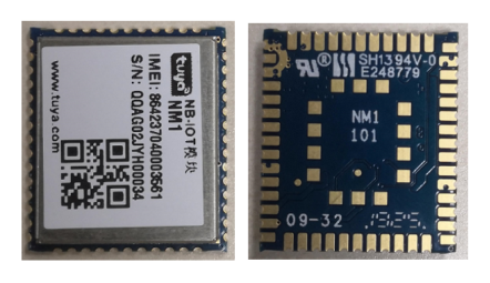
Module appearance
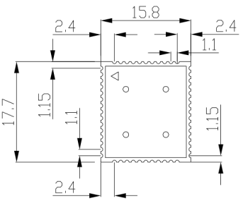
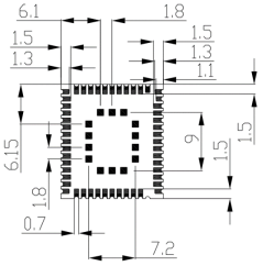
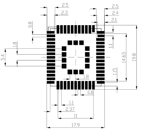
Package dimensions
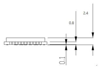
NM1 is equipped with a total of 66 pins, including 52 LCC pins and 14 LGA pins. It has an ultra-compact profile of 17.7 mm (L) x 15.8 mm (W) x 2.4 mm (H).
Features
The following table describes the detailed features of NM1 in terms of physical characteristics, baseband, RF, technical standards, and environmental specifications.
Key features
| Items | Features | Details |
|---|---|---|
| Physical characteristics | Dimensions and packages | NM1 is equipped with a total of 66 pins, including 52 LCC pins and 14 LGA pins. It has an ultra-compact profile of 17.7 mm (L) x 15.8 mm (W) x 2.4 mm (H). |
| Module | Platform | MediaTek MT2625 |
| Module | Processor architecture | Arm Cortex-M4 |
| Module | USIM | 1.8V SIM card |
| Module | USB port | USB 1.1 |
| Module | Voltage | |
| Module | Operating mode | PWRKEY or PSM_EINT to wake up the module from PSM. |
| Module | Power saving | The module consumes an ultra-low current (typically 3.5 μA) in PSM. PSM is designed to reduce the power consumption of the module and improve battery life. |
| Module | UART interfaces | |
| Module | RTC | Supported |
| Module | ADC | The module provides a 10-bit ADC input channel to read the voltage value. The interface is available in Active and Idle mode. |
| Module | Ring indication (RI) signal* | When there is an SMS or URC output, the module will inform DTE with the RI pin. |
| Module | Network status indication | This pin keeps in high level in Active and Idle mode and in low level during module’s power-off or in PSM. |
| RF | Protocol | Conforming to the NB-IoT radio protocols in 3GPP Release 13 |
| RF | Max transmitting power | 23 dBm ± 2 dB |
| RF | Receiving sensitivity | -123 dBm/15 kHz (non-retransmit) |
| RF | Antenna interface | 50Ω impedance control. The antenna is supplied by a third party. |
| Technical standards | Data transmission | Single-tone: 25.5 kbps (downstream)/16.7 kbps (upstream). Multi-tone: 25.5 kbps (downstream)/62.5 kbps (upstream). |
| Technical standards | Network protocols | UDP/TCP/CoAP/LwM2M/PPP*/SSL*/DTLS*/FTP*/HTTP*/MQTT/HTTPS* |
| Environmental specifications | Temperature | Operation temperature range: -35°C to +75°C 1) Extended temperature range: -40°C to +85°C 2) Storage temperature range: -40°C to +90°C |
| Applications | SMS messages* | Text and PDU mode |
| Applications | Firmware update | Update firmware via main UART port OTA update (considering the update time and battery level) |
Note
- 1) Within the operation temperature range, the module is 3GPP compliant.
- 2) Within the extended temperature range, the module remains the ability to operate properly. There are no effects on the radio spectrum and no harm to the radio network. Only the values of one or more parameters like output power might exceed the specified tolerances of 3GPP specifications. When the temperature returns to the normal operating temperature levels, the module will meet 3GPP specifications again.
*means under development.
Functional description
Baseband feature
The signal groups in the baseband include SIM card interface, I2C interface, UART interfaces, USB interface, network status indication, power key, reset key, PSM wake-up, GPIO interfaces, power supply, and GND.
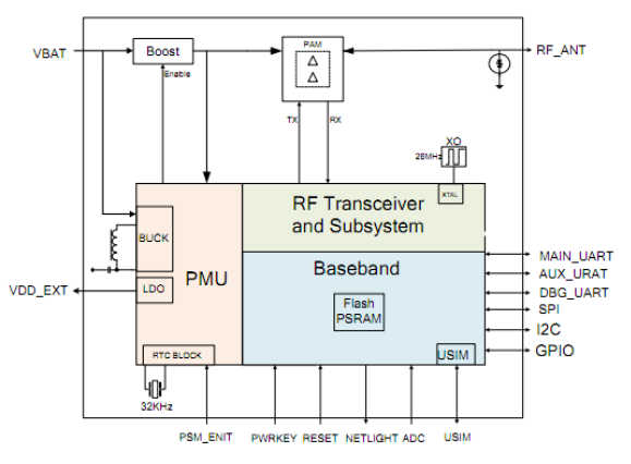
RF feature
Operating frequencies
| Operating frequencies | Upstream frequencies | Downstream frequencies |
|---|---|---|
| B1 | 1920 MHz to 1980 MHz | 2110 MHz to 2170 MHz |
| B2 | 1850 MHz to 1910 MHz | 1930 MHz to 1990 MHz |
| B3 | 1710 MHz to 1785 MHz | 1805 MHz to 1880 MHz |
| B5 | 824 MHz to 849 MHz | 869 MHz to 894 MHz |
| B8 | 880 MHz to 915 MHz | 925 MHz to 960 MHz |
| B12 | 699 MHz to 716 MHz | 729 MHz to 746 MHz |
| B13 | 777 MHz to 787 MHz | 746 MHz to 756 MHz |
| B17 | 704 MHz to 716 MHz | 734 MHz to 746 MHz |
| B18 | 815 MHz to 830 MHz | 860 MHz to 875 MHz |
| B19 | 830 MHz to 845 MHz | 875 MHz to 890 MHz |
| B20 | 832 MHz to 862 MHz | 791 MHz to 821 MHz |
| B25 | 1850 MHz to 1915 MHz | 1930 MHz to 1995 MHz |
| B26 | 814 MHz to 849 MHz | 859 MHz to 894 MHz |
| B28 | 703 MHz to 748 MHz | 758 MHz to 803 MHz |
| B66 | 1710 MHz to 1780 MHz | 2110 MHz to 2200 MHz |
RF conducted output power
| Frequency bands | Max | Min |
|---|---|---|
| B1 | 23 dBm ± 2 dB | ≤ 39 dBm |
| B2 | 23 dBm ± 2 dB | ≤ 39 dBm |
| B3 | 23 dBm ± 2 dB | ≤ 39 dBm |
| B5 | 23 dBm ± 2 dB | ≤ 39 dBm |
| B8 | 23 dBm ± 2 dB | ≤ 39 dBm |
| B12 | 23 dBm ± 2 dB | ≤ 39 dBm |
| B13 | 23 dBm ± 2 dB | ≤ 39 dBm |
| B17 | 23 dBm ± 2 dB | ≤ 39 dBm |
| B18 | 23 dBm ± 2 dB | ≤ 39 dBm |
| B19 | 23 dBm ± 2 dB | ≤ 39 dBm |
| B20 | 23 dBm ± 2 dB | ≤ 39 dBm |
| B25 | 23 dBm ± 2 dB | ≤ 39 dBm |
| B26 | 23 dBm ± 2 dB | ≤ 39 dBm |
| B28 | 23 dBm ± 2 dB | ≤ 39 dBm |
| B66 | 23 dBm ± 2 dB | ≤ 39 dBm |
RF receiving sensitivity
| Frequency bands | Conducted receiving sensitivity |
|---|---|
| B1/B2/B3/B4/B5/B8/B12/B13/B14/B17/B18/B19/B20/B25/B26/B28/B66/B70/B85 | -123 dBm/15 kHz (non-retransmit) |
Note
- The design conforms to the NB-IoT radio protocols in 3GPP Release 13 and 3GPP Release 14.
*means under development.
Operating modes
The following table describes the three operating modes of the module.
| Modes | Description |
|---|---|
| Connected | Connected: active status. The module is in this status after it is activated and connected to the network. Radio transmission and reception can be performed. If no data communication is detected for a specified time, transition to Idle mode can be initiated. |
| Idle | Idle: light sleep status. The network connection is maintained in eDRX state. Paging messages can be received. If no data communication is detected for a specified time, transition to PSM can be initiated. |
| PSM | In PSM: deep sleep status. CPU is powered off, the network is disconnected, and thus paging messages cannot be received. The module consumes an ultra-low current. The PMS duration is set by the T3324 timer. When there is upstream data to be transmitted or the tracking area update (TAU) expires, the module enters Connected mode. |
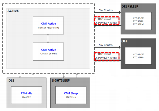
Power saving mode (PSM)
The module consumes an ultra-low current (typically 3.5 μA) in PSM. PSM is designed to reduce the power consumption of the module and improve battery life. The following figure shows the power consumption of the module in different modes.
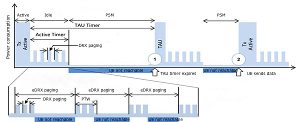
The procedure for entering PSM is as follows: The module requests to enter PSM in Attach Request message during attach or TAU procedure. Then the network accepts the request and provides values of T3324 and T3412 timers to the module and the mobile reachable timer starts. When the T3324 timer expires, the module enters PSM.
The module cannot request PSM when it is establishing an emergency attachment or initializing the public data network (PDN) connection. When the module is in PSM, it cannot be paged and stops access stratum activities such as cell re-selection, but T3412 is still active.
Either of the following methods can make the module exit from PSM:
- After the T3412 timer expires, the module will exit PSM automatically.
- Pulling down
PSM_EINT(falling edge) will wake the module up from PSM.
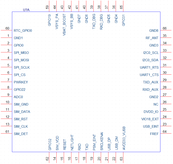
Pin description
Pin definition
I/O parameters definition
| Type | Description |
|---|---|
| I | Input |
| O | Output |
| IO | Input/Output |
Pin out
The NM1 pin out is as follows.
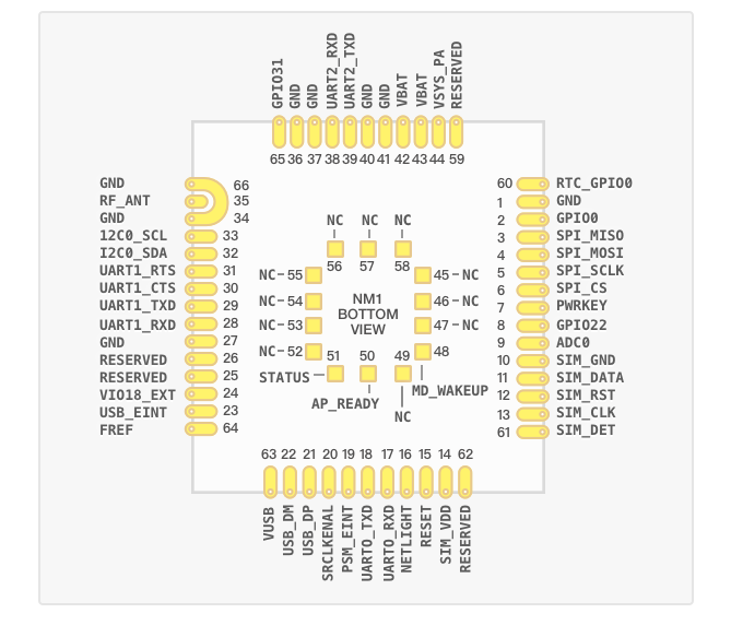
Pin description
| Pin No. | Pin name | I/O type | Input/Output | DC Characteristics | Comment |
|---|---|---|---|---|---|
| 1 | AGND | GND | - | - | |
| 2 | GPIO0 | GPIO0 | - | 1.8V | Pull down this pin to achieve USB download function. Do not pull down this pin before a normal power-on sequence. |
| 3 | SPI_MISO | Master in slave out | I | 1.8V | |
| 4 | SPI_MOSI | Master out slave in | O | 1.8V | |
| 5 | SPI_SCLK | Serial clock | O | 1.8V | |
| 6 | SPI_CS | Chip select | O | 1.8V | |
| 7 | PWRKEY | Pull down PWRKEY to turn on the module. |
I | VIL max=0.3* VBAT VIH min=0.7* VBAT |
|
| 8 | GPIO22 | GPIO22 | - | - | |
| 9 | ADC0 | General purpose analog to digital converter interface | I | 0V to 1.4V | |
| 10 | SIM_GND | Specified ground for SIM card | - | - | |
| 11 | SIM_DATA | SIM card data signal | IO | - | |
| 12 | SIM_RST | SIM card reset signal | IO | - | |
| 13 | SIM_CLK | SIM card clock signal | IO | - | |
| 14 | SIM_VDD | SIM card power supply | O | 1.8V | |
| 15 | RESET | Reset the module. Active low. | I | - | |
| 16 | NETLIGHT | Network status indication | O | - | A GPIO that can be used to indicate network status. |
| 17 | UART0_RXD | Receive data from the external microcontroller. | I | 1.8V | |
| 18 | UART0_TXD | Transmit data to the external microcontroller. | O | 1.8V | |
| 19 | PSM_EINT | Dedicated external interrupt pin, used to wake up the module from PSM. | I | - | |
| 20 | SRCLKENAI | NFC interface | - | 1.8V | |
| 21 | USB_DP | USB differential data (+) | - | - | |
| 22 | USB_DM | USB differential data (-) | - | - | |
| 23 | USB_EINT | USB_EINT | |||
| 24 | VIO18_EXT | 1.8V output power supply. No voltage output in PSM. | O | Vmin=1.53V Vnorm=1.8V |
|
| 25 | DVDD_IO | NC | NC | NC | |
| 26 | NC | NC | - | - | |
| 27 | GND | GND | - | - | |
| 28 | UART1_RXD | Receive data through serial communication by default. | I | 1.8V | |
| 29 | UART1_TXD | Transmit data through serial communication by default. | O | 1.8V | |
| 30 | UART1_CTS | Specify whether to receive data. | - | 1.8V | |
| 31 | UART1_RTS | Specify whether to transmit data. | - | 1.8V | |
| 32 | I2C0_SDA | I2C serial data line | IO | - | |
| 33 | I2C0_SCL | I2C serial clock line | O | - | |
| 34 | GND | GND | - | - | |
| 35 | RF_ANT | RF antenna interface | 50Ω characteristic impedance | ||
| 36 | GND | GND | - | - | |
| 37 | GND | GND | - | - | |
| 38 | UART2_RXD | The logging port for receiving data. | I | 1.8V | |
| 39 | UART2_TXD | Transmit log data. | O | 1.8V | |
| 40 | GND | GND | - | - | |
| 41 | GND | GND | - | - | |
| 42 | VSYS_BB | Input power | I | Vmin=2.1V Vnorm=3.3V Vmax=3.63V |
|
| 43 | VBAT_BOOST | Input power | I | Vmin=2.1V Vnorm=3.3V Vmax=3.63V |
|
| 44 | VSYS_PA | Output power | O | 3.3V | |
| 45 | GPIO11 | Reserved | - | 1.8V | |
| 46 | GPIO10 | Reserved | - | 1.8V | |
| 47 | GPIO25 | Reserved | - | 1.8V | |
| 48 | MD_WAKEUP | - | - | - | |
| 49 | GPIO28 | Reserved | - | 1.8V | |
| 50 | AP_READY | - | - | - | |
| 51 | STATUS | - | - | - | |
| 52 | GPIO24 | Reserved | - | 1.8V | |
| 53 | GPIO34 | Reserved | - | 1.8V | |
| 54 | GPIO33 | Reserved | - | 1.8V | |
| 55 | GPIO21 | Reserved | - | 1.8V | |
| 56 | GPIO20 | Reserved | - | 1.8V | |
| 57 | GPIO8 | Reserved | - | 1.8V | |
| 58 | GPIO1 | Reserved | - | 1.8V | |
| 59 | GPIO19 | Reserved | - | 1.8V | |
| 60 | RTC_GPIO0 | - | - | - | |
| 61 | SIM_DET | Detect the SIM card. | - | - | SIM card detection is supported currently. Leave this pin floating. |
| 62 | GPIO32 | Reserved | - | 1.8V | |
| 63 | AVDD33_VUSB | - | I | - | |
| 64 | FREF | The base frequency | I | - | |
| 65 | GPIO31 | Reserved | - | 1.8V | |
| 66 | GND | GND | - | - |
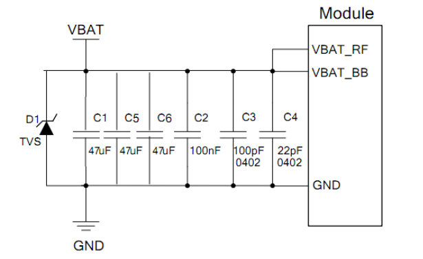
Power supply pins
Pin description
NM1 can be powered by a battery or an external power supply. The ground pin and signal ground pin must be connected to the ground plane on the PCB. Otherwise, the overall performance of the module might be affected.
| Pin No. | Signal | Description | Min | Typical | Max | Unit |
|---|---|---|---|---|---|---|
| 42 | VBAT_BOOST | Input power | 2.1 | 3.3 | 3.63 | V |
| 43 | VSYS_BB | Input power | 2.1 | 3.3 | 3.63 | V |
| 44 | VSYS_PA | Output power | - | 3.3 | - | V |
| 1, 27, 34, 36, 37, 40, 41 | GND | GND | - | - | - | - |
Power supply requirements
The supply voltage of the module ranges from 2.1V to 3.6V. You can use a low quiescent current LDO with an output current capacity of 0.5A as the power supply. A LiMnO2 battery can also be used as the power supply.
- Voltage drop: When the module is working, make sure its input voltage will never drop below 2.1V. Otherwise, the module cannot work properly.
- Voltage regulator and filter capacitor: It is recommended to place a 100 μF tantalum capacitor with low ESR (ESR < 0.7Ω) and three ceramic capacitors (100 nF, 100 pF 0402, and 22 pF 0402) near the VBAT pins.
- Electrostatic discharge protection: Add a TVS diode on the VBAT trace (near VBAT pins) to improve surge voltage withstand capability.
- In principle, the longer the VBAT trace is, the wider it should be.
A reference circuit for the power supply is illustrated in the following figure.
Power on/reset/PSM exit
Pin description
| Pin No. | Signal | Features |
|---|---|---|
| 7 | PWRKEY | Power on the module. |
| 15 | RESET | Reset the module. |
| 19 | PSM_EINT | Dedicated external interrupt pin, used to wake up the module from PSM. |
Applications
-
Power on: The module will be powered on after the
PWRKEYpin is driven to a low level for at least 35 ms and then pulled up or left floating.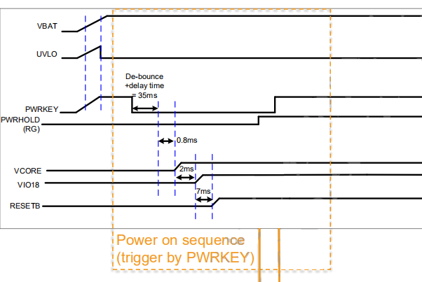
-
Reset: The module will be reset after the
RESETpin is driven to a low level for at least 35 ms and then pulled up or left floating. -
PSM exit: Pulling down
PSM_EINT(falling edge) will wake the module up from PSM. A low pulse width of at least 4 ms is required, as shown in the timing diagram below. If a triode is used to wake up the module, the output pin must not be pulled up. When MCU’s GPIO wakes up the module, use an open-drain output pin. Otherwise, the supply voltage drop might be mistaken for low-level output.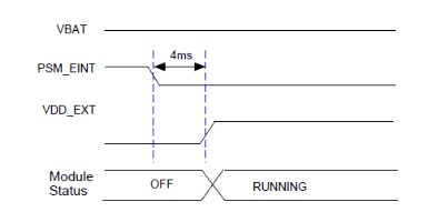
-
Pull down
PWRKEYorPSM_EINTto wake up the module from PSM. In PSM, theRESETpin is not available.
-
Use an open drain/collector driver to control the
RESETpin.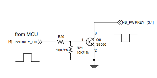
-
Use a button to control the
RESETpin.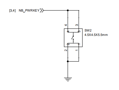
-
The module is powered on automatically and
PWRKEYis driven to high level.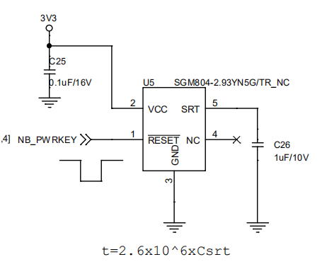
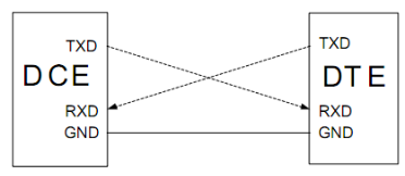
UART interfaces
Pin description
The module provides three UART ports:
- Download port: used for firmware update and AT command communication. The baud rate is 115200 bps by default and is 921600 bps when the port is used for firmware update.
- User port: used for communicating with an external microcontroller. The baud rate can be 115200 bps or 9600 bps.
- Logging port: used for firmware debugging and log printing.
The user port is the default port for communicating with an external microcontroller through Tuya’s serial protocol.
| Pin No. | Signal | Features |
|---|---|---|
| 17 | UART0_RXD | Receive firmware updates. |
| 18 | UART0_TXD | Transmit firmware updates. |
| 28 | UART1_RXD | The user port for receiving data. |
| 29 | UART1_TXD | The user port for transmitting data. |
| 38 | UART2_RXD | The logging port for receiving data. |
| 39 | UART2_TXD | The logging port for transmitting data. |
Applications
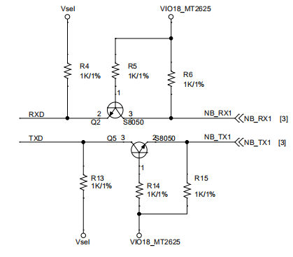
The module provides 1.8V UART interfaces. A level translator should be used if the application is equipped with a 3.3V UART interface. Take a level translator UM3202 as an example to show the reference design.
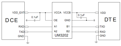
Alternatively, use a triode to translate voltage level.
See the circuit diagram above for how the logging port, user port, and download port are connected.
SIM interface
Pin description
| Pin No. | Pin name | Description | Comment |
|---|---|---|---|
| 11 | SIM_DATA | Data signal of SIM card | Voltage accuracy: 1.8V±5%. Maximum supply current: about 60 mA. |
| 13 | SIM_CLK | Clock signal of SIM card | Voltage accuracy: 1.8V±5%. Maximum supply current: about 60 mA. |
| 12 | SIM_RST | Reset signal of SIM card | Voltage accuracy: 1.8V±5%. Maximum supply current: about 60 mA. |
| 14 | SIM_VDD | Power supply for SIM card | Voltage accuracy: 1.8V±5%. Maximum supply current: about 60 mA. |
Applications

Circuit design
- Place the SIM card connector near the module. Keep the trace length as less than 200 mm as possible.
- Place a 1 μF decouple capacitor between
SIM_VDDand GND, close to the SIM card connector. - Place a 10 to 20K pull-up resistor on the
SIM_DATA. - Place the RF bypass capacitors (33 pF) close to the SIM card connector on all signal traces (
SIM_DATA,SIM_RST, andSIM_CLK) to improve EMI suppression. - Keep SIM card signals away from RF and VBAT traces. To avoid crosstalk between
SIM_DATAandSIM_CLK, keep them away from each other. - In order to offer good ESD protection, it is recommended to add a TVS diode array with a parasitic capacitance of less than 50 pF. The ESD protection device should be placed as close to the SIM card connector as possible, and make sure the SIM card signal lines go through the ESD protection device first and then to the module.
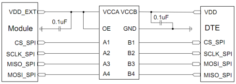
SPI interface
Pin description
| Pin No. | Signal | Features |
|---|---|---|
| 3 | SPI_MISO | Master in slave out |
| 4 | SPI_MOSI | Master out slave in |
| 5 | SPI_ SCLK | SPI serial clock |
| 6 | SPI_CS | SPI chip select |
NM1 SPI supports slave mode only. NM1-CT SPI supports both master and slave mode.
Applications
The module provides 1.8V SPI interface. A level translator for SPI should be used if the application is equipped with a 3.3V UART interface.
A reference circuit is illustrated in the following figure.
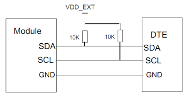
I2C bus
Pin description
| Pin No. | Signal | Features |
|---|---|---|
| 32 | SDA | I2C serial data line |
| 33 | SCL | I2C serial clock line |
I2C is a simple serial communication bus protocol that uses just two bus wires, a serial data wire (SDA) and a serial clock wire (SCL). I2C is integrated into many ICs and allows devices to communicate directly with each other. Each device is recognized by a unique address to differentiate from other devices on the same I2C bus and can operate either as a transmitter or a receiver depending on its function.
Applications
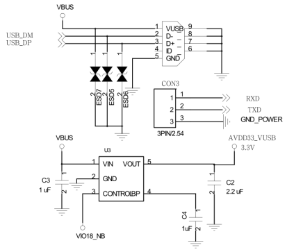
USB interface
Pin description (COM not supported)
The USB interface conforms to USB 1.1 specifications and can only be used for the software update. Pay attention to the influence of junction capacitance of ESD protection components on USB data lines. Typically, the capacitance value should be less than 0.5 pF. The impedance of the USB differential trace should be 90Ω.
| Pin No. | Signal | Features |
|---|---|---|
| 2 | GPIO0 | Pull down this pin to achieve USB download function. |
| 21 | USB_DP | USB differential data (+). |
| 22 | USB_DM | USB differential data (-). |
| 63 | AVDD33_VUSB | AVDD33_VUSB |
Applications
-
The nominal input voltage of the NM1 module is 3.3V. When the USB download function is used, design an LDO circuit to regulate the voltage to 3.3V.
-
Pull down
GPIO0to achieve USB download function. -
Make sure to route the USB signal traces as differential pairs with total grounding. The impedance of USB differential trace is 90Ω.
-
Do not route signal traces under the power supply, RF signal traces, and other sensitive signal traces. It is important to route the USB differential traces in the inner layer with ground shielding on not only the upper and lower layers but also the right and left sides.
-
Keep the ESD protection components as close to the USB connector as possible. Typically, the parasitic capacitance value of the ESD device on USB data lines should be less than 3 pF.
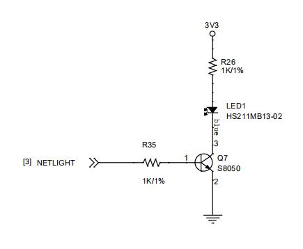
Network status indication
Netlight interface
| Pin No. | Signal | Features |
|---|---|---|
| 16 | NETLIGHT | This pin keeps in high level in Connected and Idle status and in low level in discharging or PSM. |
Applications
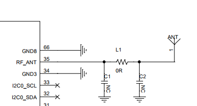
Antenna interface
Pin description
| Pin No. | Signal | Features |
|---|---|---|
| 35 | RF_ANT | 50Ω characteristic impedance |
Antenna matching circuit
In order to achieve better RF performance, it is recommended to place the π-type matching components as close to the antenna as possible.
By default, the capacitors (C1/C2) are not mounted and a 0Ω resistor is mounted on L1.
RF layout
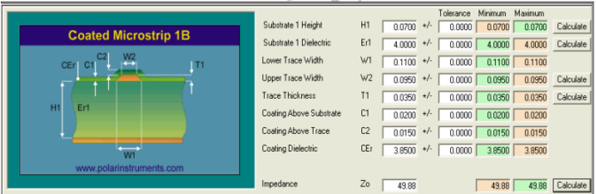
For your MCU PCB, the characteristic impedance of all RF traces should be controlled as 50Ω. A microstrip line is used for impedance control.
Microstrip line design on PCB
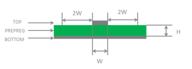
Principles in RF layout design:
- The distance between the RF pins and the RF connector should be as short as possible. All the right angle traces should be changed to 135° or curved ones.
- The reference ground of RF traces should be complete. Add some ground vias around RF traces. The distance between the ground vias and RF traces should be no less than two times the width of RF signal traces.
- The GND pins are adjacent to RF pins and should be fully connected to the ground.
- There should be a distance between the pad connected to the signal pin and the ground plane.
- Use impedance simulation tool to control the characteristic impedance of RF traces as 50Ω.
The following figure provides parameters used for impedance control. You can adjust the trace width properly to get the trace impedance closer to 50Ω.
Antenna requirements
Antenna cable insertion loss requirements
| Frequency bands | Requirements |
|---|---|
| B5/B8/B12*/B13*/B17*/B18*/B19*/B20/B26*/B28* | Cable insertion loss: < 1 dB |
| B1/B2*/B3/B25*/B66* | Cable insertion loss: < 1.5 dB |
Antenna parameters requirements
| Parameters | Requirements |
|---|---|
| Frequency bands | Vary depending on the requirements of the local operators. |
| Voltage standing wave ratio (VSWR) | ≤ 2 |
| Efficiency | ≥ 30% |
| Max input power (W) | 50 |
| Input impedance (Ω) | 50 |
| Polarization | Linear polarization |
Antenna design requirements
- The antenna should be kept away from components that are more likely to generate EMI, such as power source and data line.
- To maximize the RF performance, the distance between the antenna and the PCB or mental materials should be at least 15 mm.
- Make sure that the enclosure surrounding the antenna is not metal materials. Otherwise, the radiation performance might be degraded. It is recommended to hollow out the breakout board around the antenna area.
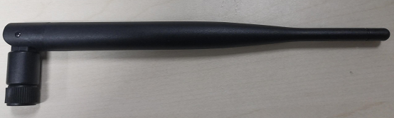
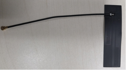
Antenna type
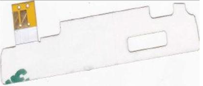
This module does not come with an antenna so an external antenna is required. You can choose one from the external rubber antenna, helical antenna, FPC antenna with IPEX connector, and PCB antenna. The antenna type can be monopole, planar inverted‐F antenna (PIFA), inverted‐F antenna (IFA), loop, and more.
The following figure shows the common antennas.
Rubber antenna
FPC antenna with IPEX connector
Built-in FPC antenna
Reliability design
EMC and ESD suppression design guide
Electromagnetic compatibility (EMC) is one of the essential considerations in designing for signal integrity and power integrity.
- When you design the peripheral circuit, have two times the width of the trace when routing signals close to each other to minimize noise coupling and generation.
- Place decoupling capacitors close to voltage pins. Keep the high-frequency and high-speed circuits and sensitive circuits away from the edge of the PCB. To reduce crosstalk between signals, increase the spacing between the traces. Provide shielding for components that emit RFI and EMI waves to protect sensitive signals from interference.
Design considerations for ESD circuit protection.
- Place ESD protection devices close to the critical signal I/Os, such as the SIM card.
- In PCB layout and design, make sure the metal shielding enclosure is fully connected to the ground.
PCB pad design
It is recommended to design the 14 pads placed in the middle of the PCB as per the dimensions specified in the structure diagram. Extend the 52 pads around the PCB to the module for over 0.3 mm and the other three sides of the pads for 0.05 mm.
Thermal design
The module generates heat when it works or might be affected by high-temperature components. The module design ensures good heat dissipation. When connecting the module to the PCB, connect the thermal pad to the ground properly to ensure thermal conduction and balance and better electrical performance.
Note
- Place the module away from the power supply and high-speed signals and protect the traces of sources of EMI.
- Place the antenna and the coaxial cable that is used to connect the antenna and network interface controller (NIC) away from these sources of EMI.
- Place the module away from components that generate a large amount of heat such as the CPU. Otherwise, the RF performance might be degraded.
Packing and manufacturing
Mechanical dimensions
NM1 is equipped with a total of 66 pins, including 52 LCC pins and 14 LGA pins.
The dimensions are 17.7 mm (L) x 15.8 mm (W) x 2.4 mm (H), as shown below.

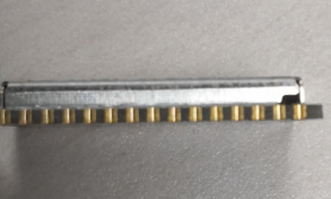
Side view
Pin out
SMT package
Top/bottom/side view
The tolerances for dimensions of length and width, height, and PCB thickness are ±0.35 mm, ±0.2 mm, and ±0.1 mm respectively. If you have special requirements for dimensions, please specify them in the datasheet after consultations.
Is this page helpful?
YesFeedbackIs this page helpful?
YesFeedback


