TYZS9V Module Datasheet
Last Updated on : 2021-06-09 04:13:31download
Product Overview
TYZS9V is a low power-consuming embedded Zigbee module developed by Hangzhou Tuya Information Technology Co., Ltd. It consists of a highly integrated wireless radio processor chip (EFR32MG13P732IM48-C) and several peripherals, with a built-in 802.15.4 PHY/MAC Zigbee network protocol stack and robust library functions. TYZS9V is embedded with a 32-bit low power-consuming ARM Cortex-M4 core, 512 KB flash, 64 KB RAM data memory, and robust peripheral resources. TYZS9V runs on the FreeRTOS platform that integrates all Zigbee MAC library functions. You can develop built-in Zigbee products as required. Figure 1 shows the architecture of TYZS9V. 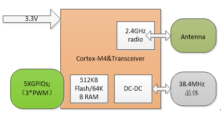 Figure 1 TYZS9V architecture
Features
- Built-in 32-bit low power-consuming ARM Cortex-M4 core with DSP instructions and floating-point unit functioning as an application processor Basic frequency: 40 MHz supported
- Wide working voltage: 1.8 V to 3.8 V
- Peripherals: five GPIOs, including three PWMs
- Zigbee operating feature 802.15.4 MAC/PHY supported Working channel: 11 to 26 @2.400 GHz to 2.483 GHz, with an air interface rate of 250 kbit/s Built-in DC-DC circuit, maximizing the power supply conversion efficiency Maximum output power: +19 dBm; dynamic output power: > 35 dB Runtime power consumption: 63 µA/MHz; current in sleep mode: 1.4 µA Proactive network configuration for terminals Embedded onboard PCB antenna Working temperature: -40℃ to 105℃ AES 128/256-based hardware encryption
Major Application Fields
- Intelligent building
- Intelligent home and household applications
- Intelligent socket and smart lighting
- Industrial wireless control
- Healthcare and measurement
- Asset tracing
Module Interfaces
Dimensions and Pin Layout
TYZS9V provides two rows of pins with the distance of 2.0 mm between every two pins. TYZS9V size: 26 mm (W) x 16 mm (L) x 1 mm (H) Figure 2 shows the overall pin layout of TYZS9V. 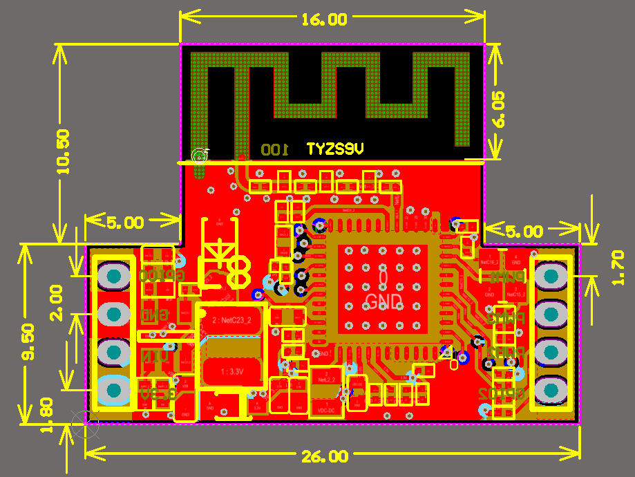 Figure 2 Front and back views of TYZS9V
Pin Definition
Table 1 describes the interface pins. Table 1 TYZS9V interface pins | No. | Symbol | I/O Type | Functions | | ------------ | -------- | ------------ | ------------------------------------------------------------ | | P1.1 | GPIO0 | I/O | Functions as a GPIO, corresponding to the PA3 pin of the internal IC. | | P1.2 | GND | P | Module reference ground pin | | P1.3 | VIN | P | A pin for external DC power supply and supports a maximum of 30 V DC power supply. | | P1.4 | 3.3V | P | A pin for 3.3 V voltage and can be used to output 3.3 V power supply. | | P2.1 | PWM1 | I/O | Functions as a GPIO and can output PWM signals to control lights. It corresponds to the PF5 pin of the internal IC. | | P2.2 | PWM3 | I/O | Functions as a GPIO and can output PWM signals to control lights. It corresponds to the PF4 pin of the internal IC. | | P2.3 | PWM2 | I/O | Functions as a GPIO and can output PWM signals to control lights. It corresponds to the PA2 pin of the internal IC. | | P2.4 | GPIO2 | I/O | Functions as a GPIO, corresponding to the PA5 pin of the internal IC. | | TP1 | nRST | I | Hardware reset pin, and the chip is reset when the level is low. TYZS9V has a power-on reset function, and this pin is not necessary in the actual situation. | | TP2 | ADC | AI | ADC port(1),12-bit precision SAR analog-to-digital converter. | | TP3 | SWCLK | I/O | JLINK SWCLK programming pin, which can also be used as a GPIO in normal programs. | | TP6 | SWDIO | I/O | JLINK SWDIO programming pin, which can also be used as a GPIO in normal programs. | | TP5 | TXD | O | UART0_TXD communication interface, corresponding to the PA0 pin of the internal IC. | | TP4 | RXD | I | UART0_RXD communication interface, corresponding to the PA1 pin of the internal IC. | Note: P indicates power-supply pins, I/O indicates input/output pins, and AI indicates analog input pins. nRST is only a module hardware reset pin, which cannot clear the Zigbee network configuration. (1): This pin can only be used as an ADC interface and cannot be used as a common I/O pin. If this pin is not used, it must be disconnected. When this pin is used as the ADC input interface, the input voltage range must be 0 to AVDD, which can be configured using software.
Test Pin Definition
Table 2 describes the test pins. Table 2 TYZS9V test pins
| No. | Symbol | I/O Type | Functions |
|---|---|---|---|
| - | - | I | Used for the module production test. |
Note: It is recommended that test pins not be used.
Electrical Parameters
Absolute Electrical Parameters
Table 3 Absolute electrical parameters
| Parameter | Description | Minimum Value | Maximum Value | Unit |
|---|---|---|---|---|
| Ts | Storage temperature | -50 | 150 | ℃ |
| VCC | Power-supply voltage | -0.3 | 3.8 | V |
| Static electricity voltage (human model) | TAMB -25℃ | - | 2.5 | kV |
| Static electricity voltage (machine model) | TAMB -25℃ | - | 0.5 | kV |
Electrical Conditions
Table 4 Normal electrical conditions
| Parameter | Description | Minimum Value | Typical Value | Maximum Value | Unit |
|---|---|---|---|---|---|
| Ta | Working temperature | -40 | - | 105 | ℃ |
| VIN | Working voltage | 5.0 | 28 | 30 | V |
| VIL | I/O low-level input | -0.3 | - | VCC x 0.25 | V |
| VIH | I/O high-level input | VCC x 0.75 | - | VCC | V |
| VOL | I/O low-level output | - | - | VCC x 0.1 | V |
| VOH | I/O high-level output | VCC x 0.8 | - | VCC | V |
| Imax | I/O drive current | - | - | 12 | mA |
Note: The typical VCC voltage is 3.3 V.
Zigbee TX Power Consumption
Table 5 TX power consumption during constant emission
| Symbol | Rate | Tx power | Typical Value | Unit |
|---|---|---|---|---|
| IRF | 250 kbit/s | +19 dBm | 19.9 | mA |
| IRF | 250 kbit/s | +12 dBm | 8.6 | mA |
| IRF | 250 kbit/s | +10 dBm | 6.6 | mA |
| IRF | 250 kbit/s | +7 dBm | 5.6 | mA |
| IRF | 250 kbit/s | +0 dBm | 3.4 | mA |
Note: When the preceding data is being tested, the duty cycle is set to 100%, and the power-supply voltage is set to 30 V.
Zigbee RX Power Consumption
Table 6 RX power consumption during constant receiving
| Symbol | Rate | Typical Value | Unit |
|---|---|---|---|
| IRF | 250 kbit/s | 2.4 | mA |
Note: When VIN is set to 30 V, the UART is in the active state.
Power Consumption in Operating Mode
Table 7 TYZS9V working current | Working Mode | Working Status (Ta = 25℃) | Average Value | Maximum Value | Unit | | ------------ | ------------------------------ | ---------- | ---------- | -------- | | EZ mode | The module is in the EZ state. | 3 | 10 | mA | | Operating mode | The module is in the connected state. | 1.2 | 2 | mA | | Deep sleep mode | The module is in the deep sleep mode, with the 64 KB flash. | 1.4 | 3 | uA |
RF Features
Basic RF Features
Table 8 Basic RF features
| Parameter | Description |
|---|---|
| Frequency band | 2.400 GHz to 2.484 GHz |
| Physical layer standard | IEEE 802.15.4 |
| Data transmission rate | 250 kbit/s |
| Antenna type | Onboard PCB antenna |
| Line-of-sight transmission distance | > 120 m |
Zigbee Output Performance
Table 9 TX continuous transmission performance
| Parameter | Minimum Value | Typical Value | Maximum Value | Unit |
|---|---|---|---|---|
| Maximum output power | - | +19 | - | dBm |
| Minimum output power | - | -30 | - | dBm |
| Output power adjustment step | - | 0.5 | 1 | dB |
| Frequency error | -15 | - | +15 | ppm |
| Output spectrum adjacent-channel rejection ratio | -31 | dBc |
Note: The maximum output power can reach +19 dBm. The power output can be adjusted under normal use. The high-power output can be used for overlay transmission in extremely complex conditions, such as modules embedded in a wall.
Zigbee RX Sensitivity
Table 10 RX sensitivity
| Parameter | Minimum Value | Typical Value | Maximum Value | Unit | |
|---|---|---|---|---|---|
| PER < 10%, RX sensitivity, 250 kbit/s@OQPSK | - | -101 | - | dBm |
Antenna Information
Antenna Types
By default, the onboard PCB antenna is used. The antenna gain is about 2.0 dBi.
Antenna Interference Reduction
When you use an onboard PCB antenna on a Zigbee module, make sure that the antenna on the module is at least 15 mm away from other metal parts to ensure optimal wireless performance. It is recommended that the antenna location on the PCB be hollowed out. To prevent negative effect on antenna radiation performance, do not route copper or cable wires along the antenna area of the user PCB board.
Packaging Information and Production Instructions
Mechanical Dimensions
For details about the dimensions, see Figure 2.
Recommended PCB Encapsulation
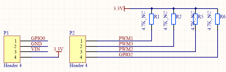 Figure 3 TYZS9V diagram with pins
Production Instructions
Storage conditions of a delivered module are as follows:
- The anti-moisture bag must be placed in an environment where the temperature is under 30°C and the relative humidity is under 85%.
- The shelf life of a dry-packaged product is six months from the date when the product is packaged and sealed. Precautions:
- Throughout the production process, each involved operator must wear an electrostatic ring and electrostatic clothes.
- During the operation, strictly protect the module from water and strains.
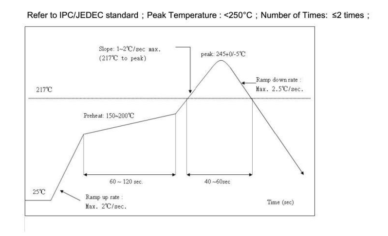
Recommended Oven Temperature Profile
Is this page helpful?
YesFeedbackIs this page helpful?
YesFeedback


