WBRG1 模组规格书
更新时间:2024-04-24 09:59:49下载pdf
WBRG1 是由涂鸦智能开发的一款低功耗嵌入式 Wi-Fi +蓝牙模组。它由一个高集成度的无线射频芯片 RTL8721CSM 和外扩 flash 芯片构成,内置了 Wi-Fi 网络协议栈和丰富的库函数。
产品概述
WBRG1 包含 KM4 MCU 和低功耗的 KM0 MCU,WLAN MAC,1T1R WLAN,最高主频200MHz,内置 4Mbyte PSRAM,8Mbyte flash 和丰富的外设资源。
WBRG1 是一个 RTOS 平台,集成了所有 Wi-Fi MAC 以及 TCP/IP 协议的函数库。用户可以基于这些开发满足自己需求的嵌入式 Wi-Fi 产品。
特性
- 内置低功耗 32 位 Cortex-M33 CPU,可以兼作应用处理器
- 最大主频支持 200MHz
- 工作电压:3.0V–3.6V
- 外设:6 × PWM,3 × UART,1 × I2C,1 × PTA,1 × Audio
- Wi-Fi/BT 连通性
- 802.11 b/g/n20/n40
- 通道 1-14@2.4GHz(CH1-11 for US/CA,CH1-13 for EU/CN)
- 支持 WEP/WPA/WPA2/WPA2 PSK(AES)安全模式
- 支持 Bluetooth Low Energy(蓝牙 5.0)
- 802.11b 模式下最大 +20dBm 的输出功率
- 支持 SmartConfig 和 AP 两种配网方式(包括 Android 和 iOS 设备)
- 板载 PCB 天线和外接天线 IPEX 连接器
- 工作温度:-20℃ 到 85℃
应用领域
- 智能楼宇
- 智慧家居、家电
- 智能插座、智慧灯
- 工业无线控制
- 婴儿监控器
- 网络摄像头
- 智能公交
模组接口
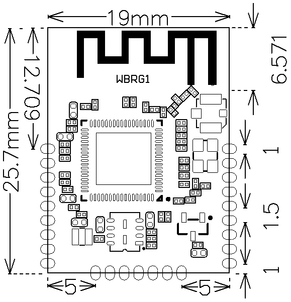
尺寸封装
-
WBRG1 共有 3 排引脚,引脚间距为 1.5mm。
-
WBRG1 尺寸大小:19±0.35 mm (W)×25.7±0.35 mm (L) ×2.9±0.15 mm (H),其中 PCB 厚度 0.8mm±0.1 mm,模组尺寸如下图所示,分别为正视图和背面图:
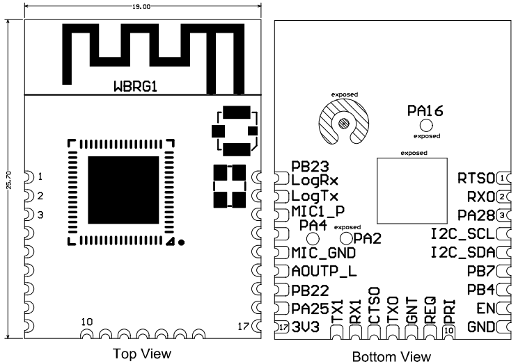
引脚定义
| 序号 | 符号 | IO 类型 | 功能 |
|---|---|---|---|
| 1 | RTS0 | I/O | PA16,芯片脚 Pin29,串口 Uart0流 控发送请求脚 |
| 2 | RX0 | I/O | PA19,芯片脚 Pin32,Uart0_RX,用户 MCU 对接串口 |
| 3 | PA28 | I/O | PA28,芯片脚 Pin38,硬件 PWM,可配置成 GPIO |
| 4 | I2C_SCL | I/O | PB5,芯片脚 Pin45,可配置成 I2C 或者 GPIO |
| 5 | I2C_SDA | I/O | PB6,芯片脚 Pin46,可配置成 I2C 或者 GPIO |
| 6 | PB7 | I/O | PB7,芯片脚 Pin47,硬件 PWM,可配置成 GPIO |
| 7 | PB4 | I/O | PB4,芯片脚 Pin44,硬件 PWM,可配置成 GPIO |
| 8 | EN | P | 模组使能脚,正常使用需要接到 3.3V,模组上已经上拉 |
| 9 | GND | P | 电源参考地 |
| 10 | PRI | I/O | PB1,芯片脚 Pin41,PTA_PRI 功能 |
| 11 | REQ | I/O | PA26,芯片脚 Pin39,PTA_REQ 功能 |
| 12 | GNT | I/O | PA27,芯片脚 Pin33,PTA_GNT 功能 |
| 13 | TX0 | I/O | PA18,芯片脚 Pin31,Uart0_TX,用户 MCU 对接串口 |
| 14 | CTS0 | I/O | PA17,芯片脚 Pin30,串口 Uart0 流控发送允许脚 |
| 15 | RX1 | I/O | PA13,芯片脚 Pin26,Uart1_RX,用户 MCU 对接串口 |
| 16 | TX1 | I/O | PA12,芯片脚 Pin25,Uart1_TX,用户 MCU 对接串口 |
| 17 | 3V3 | P | 模组的电源引脚(3.3V) |
| 18 | PA25 | I/O | PA25,芯片脚 Pin40,硬件 PWM,可配置成 GPIO |
| 19 | PB22 | I/O | PB22,芯片脚 Pin60,硬件 PWM,可配置成 GPIO |
| 20 | AOUTP_L | I/O | PB31,芯片脚 Pin65,Audio 左通道模拟输出正极 |
| 21 | MIC GND | I/O | MIC_GND |
| 22 | MIC1_P | I/O | PA4,芯片脚 Pin3,MIC1 输入正极,主 MIC |
| 23 | Log TX | I/O | PA7,芯片脚 Pin7,Log_TX,用于系统日志打印 |
| 24 | Log Rx | I/O | PA8,芯片脚 Pin8,Log_RX,用于系统日志打印 |
| 25 | PB23 | I/O | PB23,芯片脚 Pin61,硬件 PWM,可配置成 GPIO |
说明:
P表示电源引脚,I/O 表示输入输出引脚。
电气参数
绝对电气参数
| 参数 | 描述 | 最小值 | 最大值 | 单位 |
|---|---|---|---|---|
| Ts | 存储温度 | -40 | 105 | ℃ |
| VBAT | 供电电压 | -0.3 | 3.6 | V |
| 静电释放电压(人体模型) | TAMB-25℃ | - | 2 | kV |
| 静电释放电压(机器模型) | TAMB-25℃ | - | 0.5 | kV |
正常工作条件
| 参数 | 描述 | 最小值 | 典型值 | 最大值 | 单位 |
|---|---|---|---|---|---|
| Ta | 工作温度 | -20 | - | 85 | ℃ |
| VCC | 供电电压 | 3.0 | 3.3 | 3.6 | V |
| VIL | IO 低电平输入 | - | - | 0.8 | V |
| VIH | IO 高电平输入 | 2.0 | - | - | V |
| VOL | IO 低电平输出 | - | - | 0.4 | V |
| VOH | IO 高电平输出 | 2.4 | - | - | V |
| Imax | IO 驱动电流 | - | - | 16 | mA |
| Cpad | 输入引脚电容 | - | 2 | - | mA |
连续发射功耗
| 符号 | 模式 | 功率 | 平均值 | 峰值(典型值) | 单位 |
|---|---|---|---|---|---|
| IRF | 11b 11Mbps | 17dBm | 247 | 272 | mA |
| IRF | 11b 11Mbps | 18dBm | 252 | 285 | mA |
| IRF | 11g 54Mbps | 15dBm | 177 | 238 | mA |
| IRF | 11g 54Mbps | 17.5dBm | 202 | 280 | mA |
| IRF | 11n BW20 MCS7 | 13dBm | 165 | 240 | mA |
| IRF | 11n BW20 MCS7 | 16.5dBm | 192 | 269 | mA |
| IRF | 11n BW40 MCS7 | 13dBm | 144 | 236 | mA |
| IRF | 11n BW40 MCS7 | 16.5dBm | 166 | 266 | mA |
连续接收功耗
| 符号 | 模式 | 平均值 | 峰值(典型值) | 单位 |
|---|---|---|---|---|
| IRF | 11B 11M | 61 | 77 | mA |
| IRF | 11G 54M | 61 | 75 | mA |
| IRF | 11N HT20 MCS7 | 61 | 77 | mA |
工作模式下功耗
| 工作模式 | 工作状态,TA=25℃ | 平均值 | 峰值(典型值) | 单位 |
|---|---|---|---|---|
| 快连配网状态(蓝牙配网) | 模组处于快连配网状态,Wi-Fi 指示灯快闪 | 57 | 284 | mA |
| 快连配网状态(AP 配网) | 模组处于快连配网状态,Wi-Fi 指示灯慢闪 | 203 | 392 | mA |
| 快连配网状态(EZ 配网) | 模组处于快连配网状态,Wi-Fi 指示灯快闪 | 55 | 298 | mA |
| 网络连接空闲状态 | 模组处于联网工作状态,Wi-Fi 指示灯常亮 | 53 | 259 | mA |
| 网络连接操作状态 | 模组处于联网工作状态,Wi-Fi 指示灯常亮 | 56 | 293 | mA |
| 断网状态 | 模组处于断网工作状态 | 58 | 287 | mA |
说明:以上参数依据不同的固件功能,参数有所不同。
射频参数
基本射频特性
| 参数项 | 详细说明 |
|---|---|
| 频率范围 | 2.400-2.4835GHz |
| Wi-Fi 标准 | IEEE 802.11b/g/n(通道 1-14) |
| 蓝牙 标准 | 蓝牙5.0 |
| 数据传输速率 | 11b:1,2,5.5,11(Mbps) |
| 数据传输速率 | 11g:6,9,12,18,24,36,48,54(Mbps) |
| 数据传输速率 | 11n:HT20 MCS0-7 |
| 数据传输速率 | 11n:HT40 MCS0-7 |
| 天线类型 | PCB 天线,增益 1.05dBi |
发射性能
TX 连续发送性能
| 参数项 | 最小值 | 典型值 | 最大值 | 单位 |
|---|---|---|---|---|
| RF 平均输出功率,802.11b CCK Mode 11M | - | 17.5 | - | dBm |
| RF 平均输出功率,802.11g OFDM Mode 54M | - | 14.5 | - | dBm |
| RF 平均输出功率,802.11n HT20 Mode MCS7 | - | 13.5 | - | dBm |
| RF 平均输出功率,802.11n HT40 Mode MCS7 | - | 13.5 | - | dBm |
| RF 平均输出功率,蓝牙 5.0 | - | 6.5 | - | dBm |
| 频率误差 | -20 | - | 20 | ppm |
| EVM@802.11b CCK 11Mbps Mode 17.5dBm | - | - | -10 | dB |
| EVM@802.11g OFDM 54Mbps Mode 14.5dBm | - | - | -29 | dB |
| EVM@802.11n OFDM MCS7 Mode 13.5dBm | - | - | -30 | dB |
接收性能
RX 灵敏度
| 参数项 | 最小值 | 典型值 | 最大值 | 单位 |
|---|---|---|---|---|
| PER<8%,RX 灵敏度,802.11b DSSS Mode 1M | - | -97 | - | dBm |
| PER<10%,RX 灵敏度,802.11g OFDM Mode 54M | - | -76 | - | dBm |
| PER<10%,RX 灵敏度,802.11n OFDM Mode MCS7 | - | -73 | - | dBm |
天线信息
天线类型
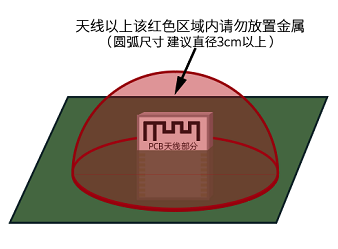
有 PCB 板载天线和外接天线两种天线接入方式。默认方式是 PCB 板载天线。
降低天线干扰
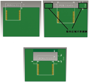
在 Wi-Fi 模组上使用 PCB 板载天线时,为确保 Wi-Fi 性能的最优化,建议模组天线部分和其他金属件距离至少在 15mm 以上。
用户 PCB 板在天线区域勿走线甚至覆铜,以免影响天线性能。
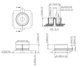
U.FL RF 连接器
U.FL RF 连接器的参数如下图所示:
上电下电时序
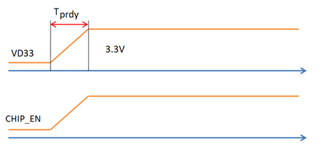
上电时序
RTL8721CSM 芯片对上电时序有要求,建议 3.3V 电压从 0V 爬升到 3.3V 的时间在 20ms 之内。
下电时序
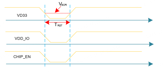
| Symbol | 参数 | 最小值 | 典型值 | 最大值 | 单位 |
|---|---|---|---|---|---|
| TPRDY | 3.3V ready time | 0.6 | - | 20 | ms |
| CHIP_EN | CHIP_EN ready time | 0.6 | - | 20 | ms |
| VBOR | BOR occurs after 3.3V is lower than this voltage | 2 | - | - | V |
| TRST | The required time that 3.3V is lower than VBOR | 1 | - | - | ms |
封装信息及生产指导
机械尺寸
PCB 尺寸大小:19±0.35mm (W)×25.7±0.35mm (L) ×0.8±0.1mm (H)。
说明:PCB 外框公差 ±0.35mm,PCB 厚度公差 ±0.1mm。
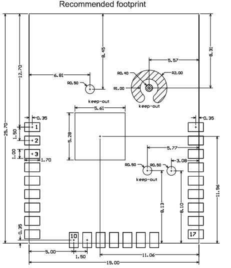
PCB 封装图
生产指南
-
涂鸦出厂的贴片封装模组建议使用 SMT 机器贴片,拆开包装后建议在 24 小时内完成焊接。如果拆封后未使用完建议放置在湿度不超过 10%RH 的干燥柜内,或重新进行真空包装并记录暴露时间。总暴露时间不超过 168 小时。
- SMT贴片所需仪器或设备:
- 贴片机
- SPI
- 回流焊
- 炉温测试仪
- AOI
- 烘烤所需仪器或设备:
- 柜式烘烤箱
- 防静电耐高温托盘
- 防静电耐高温手套
- SMT贴片所需仪器或设备:
-
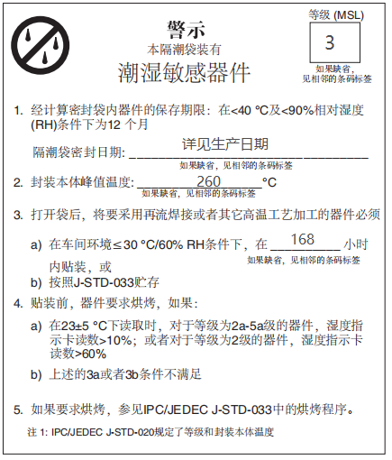
涂鸦出厂的模组存储条件如下:
-
防潮袋必须储存在温度 <40℃、湿度 <90%RH 的环境中
-
干燥包装的产品,保质期为从包装密封之日起 12 个月的时间
-
密封包装内装有湿度指示卡:
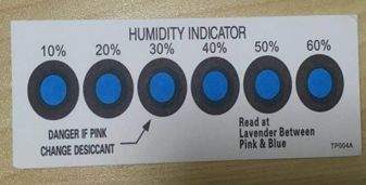
-
-
涂鸦出厂的模组当出现可能受潮的情况下需要进行烘烤:
- 拆封前发现真空包装袋破损。
- 拆封后发现包装袋内没有湿度指示卡。
- 拆封后如果湿度指示卡读取到 10% 及以上色环变为粉色。
- 拆封后总暴露时间超过 168 小时。
- 从首次密封包装之日起超过 12 个月。
-
烘烤参数如下:
- 烘烤温度:卷盘包装 40℃,小于等于 5%RH。托盘包装 125℃,小于等于 5%RH(耐高温托盘非吸塑盒拖盘)。
- 烘烤时间:卷盘包装 168 小时,托盘包装 12 小时。
- 报警温度设定:卷盘包装 50℃,托盘包装 135℃。
- 自然条件下冷却到 36℃ 以下后,即可进行生产。
- 若烘烤后暴露时间大于 168 小时没有使用完,请再次进行烘烤。
- 如果暴露时间超过 168 小时未经过烘烤,不建议使用波峰焊接工艺焊接此批次模组,因模组为 3 级湿敏器件超过允许的暴露时间很可能受潮,进行高温焊接时可能导致器件失效或焊接不良。
-
在整个生产过程中请对模组进行静电放电(ESD)保护。
-
为了确保产品合格率,建议使用 SPI 和 AOI 测试设备来监控锡膏印刷和贴装品质。
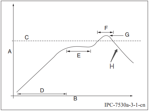
推荐炉温曲线
请根据回流焊曲线图进行温度设定,峰值温度 245℃,回流焊温度曲线如下图所示:
-
A:温度轴
-
B:时间轴
-
C:合金液相线温度:217-220℃
-
D:升温斜率:1-3℃/S
-
E:恒温时间:60-120S,恒温温度:150-200℃
-
F:液相线以上时间:50-70S
-
G:峰值温度:235-245℃
-
H:降温斜率:1-4℃/S
注意:以上推荐曲线以 SAC305 合金焊膏为例。其他合金焊膏请按焊膏规格书推荐炉温曲线设置。
储存条件
模组 MOQ 与包装信息
| 产品型号 | MOQ(pcs) | 出货包装方式 | 每个卷盘存放模组数 | 每箱包装卷盘数 |
|---|---|---|---|---|
| WBRG1 | 3600 | 载带卷盘 | 900 | 4 |
附录:声明
FCC Caution: Any changes or modifications not expressly approved by the party responsible for compliance could void the user’s authority to operate this device.
This device complies with Part 15 of the FCC Rules. Operation is subject to the following two conditions: (1) This device may not cause harmful interference, and (2) this device must accept any interference received, including interference that may cause undesired operation.
Note: This device has been tested and found to comply with the limits for a Class B digital device, according to part 15 of the FCC Rules. These limits are designed to provide reasonable protection against harmful interference in a residential installation. This device generates, uses, and can radiate radio frequency energy and, if not installed and used following the instructions, may cause harmful interference to radio communications. However, there is no guarantee that interference will not occur in a particular installation.
If this device does cause harmful interference to radio or television reception, which can be determined by turning the device off and on, the user is encouraged to try to correct the interference by one or more of the following measures:
- Reorient or relocate the receiving antenna.
- Increase the separation between the device and receiver.
- Connect the device to an outlet on a circuit different from that to which the receiver is connected.
- Consult the dealer or an experienced radio/TV technician for help.
Radiation Exposure Statement
This device complies with FCC radiation exposure limits set forth for an uncontrolled rolled environment. This device should be installed and operated with a minimum distance of 20cm between the radiator and your body.
Important Note
This radio module must not be installed to co-locate and operate simultaneously with other radios in the host system except following FCC multi-transmitter product procedures. Additional testing and device authorization may be required to operate simultaneously with other radios.
The availability of some specific channels and/or operational frequency bands are country dependent and are firmware programmed at the factory to match the intended destination. The firmware setting is not accessible by the end-user.
The host product manufacturer is responsible for compliance with any other FCC rules that apply to the host not covered by the modular transmitter grant of certification. The final host product still requires Part 15 Subpart B compliance testing with the modular transmitter installed.
The end-user manual shall include all required regulatory information/warnings as shown in this manual, including “This product must be installed and operated with a minimum distance of 20 cm between the radiator and user body”.
This device has got an FCC ID: 2ANDL-WBRG1. The end product must be labeled in a visible area with the following: “Contains Transmitter Module FCC ID: 2ANDL-WBRG1”.
This device is intended only for OEM integrators under the following conditions:
The antenna must be installed such that 20cm is maintained between the antenna and users, and the transmitter module may not be co-located with any other transmitter or antenna.
As long as the 2 conditions above are met, further transmitter tests will not be required. However, the OEM integrator is still responsible for testing their end-product for any additional compliance requirements required with this module installed.
Declaration of Conformity European Notice

Hereby, Hangzhou Tuya Information Technology Co., Ltd declares that this module product is in compliance with essential requirements and other relevant provisions of Directive 2014/53/EU,2011/65/EU. A copy of the Declaration of conformity can be found at https://www.tuya.com.

This product must not be disposed of as normal household waste, in accordance with the EU directive for waste electrical and electronic equipment (WEEE-2012/19/EU). Instead, it should be disposed of by returning it to the point of sale, or to a municipal recycling collection point.
The device could be used with a separation distance of 20cm to the human body.
该内容对您有帮助吗?
是意见反馈该内容对您有帮助吗?
是意见反馈