Zigbee SoC Board (ZTU)
The Tuya Sandwich Zigbee SoC board (ZTU) has Tuya’s ZTU Zigbee network module as a microcontroller, which is designed to help you easily prototype your IoT ideas. It can work with other circuit boards to implement specific features.
Applications
- This development board applies to a wide range of prototypes implemented with Tuya’s no-code or TuyaOS solutions.
- Develop with the board to build your IoT projects easily and fast.
- You can use this board for different development purposes.
- Embedded program development and debugging
- App development and debugging
- Creating connected devices that can be controlled with a mobile phone
- Getting started with IoT development and learning how the Zigbee-based control system works
Components
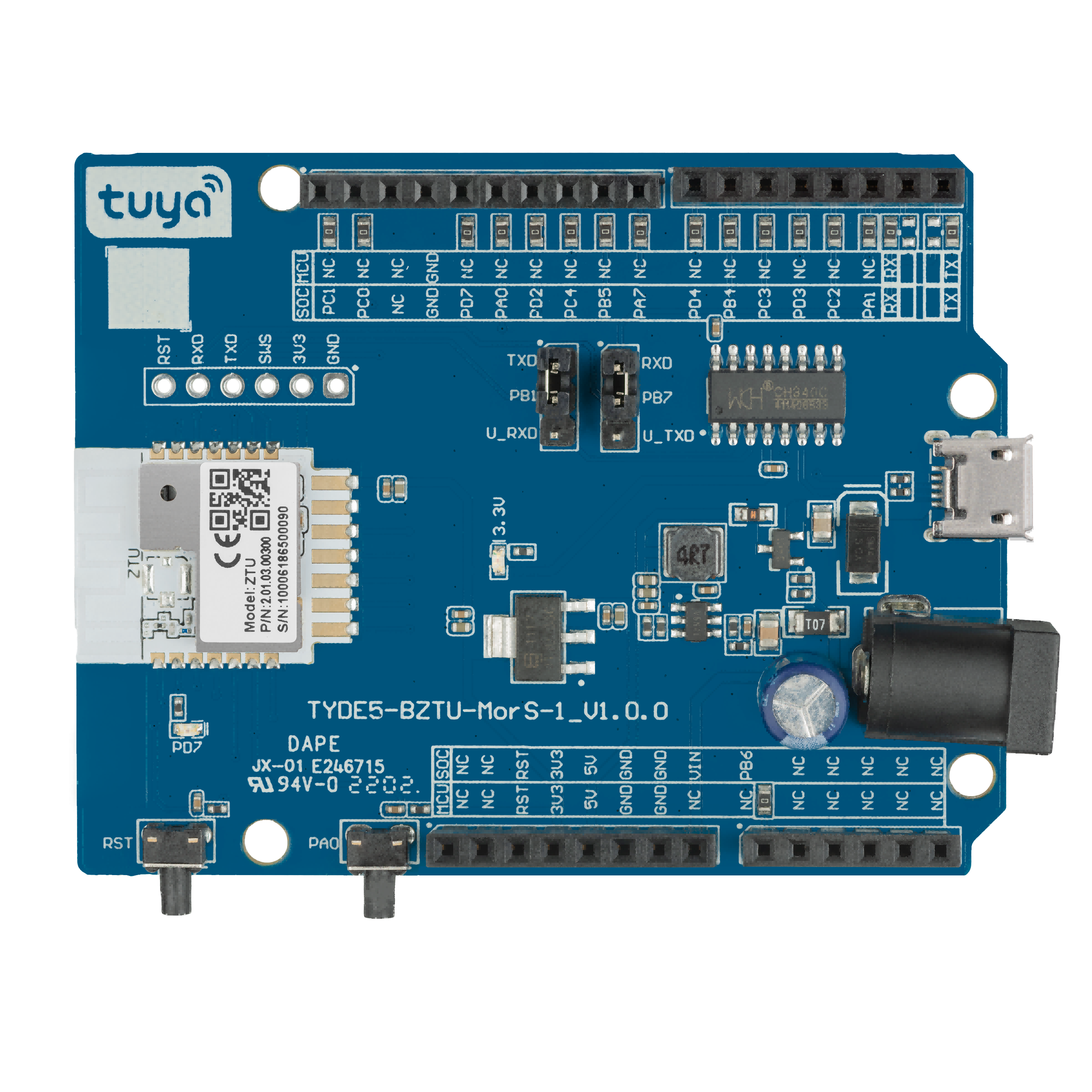
The development board is integrated with Tuya’s proprietary high-performance ZTU Zigbee module. The development board has on-board buttons, GPIOs, and a USB-to-serial chip. For more information, see the ZTU Module Datasheet.
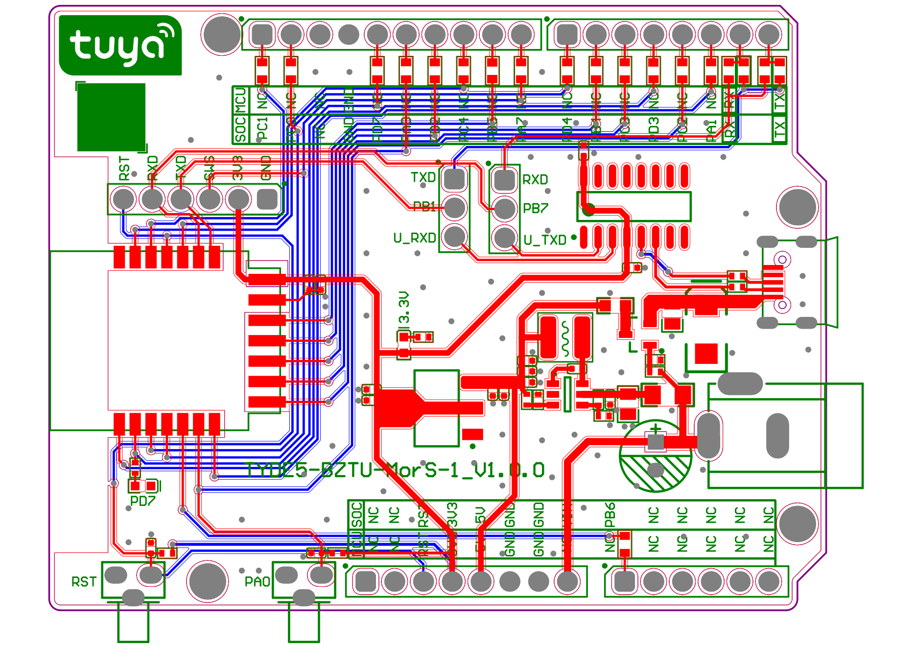
I/O port and pin description
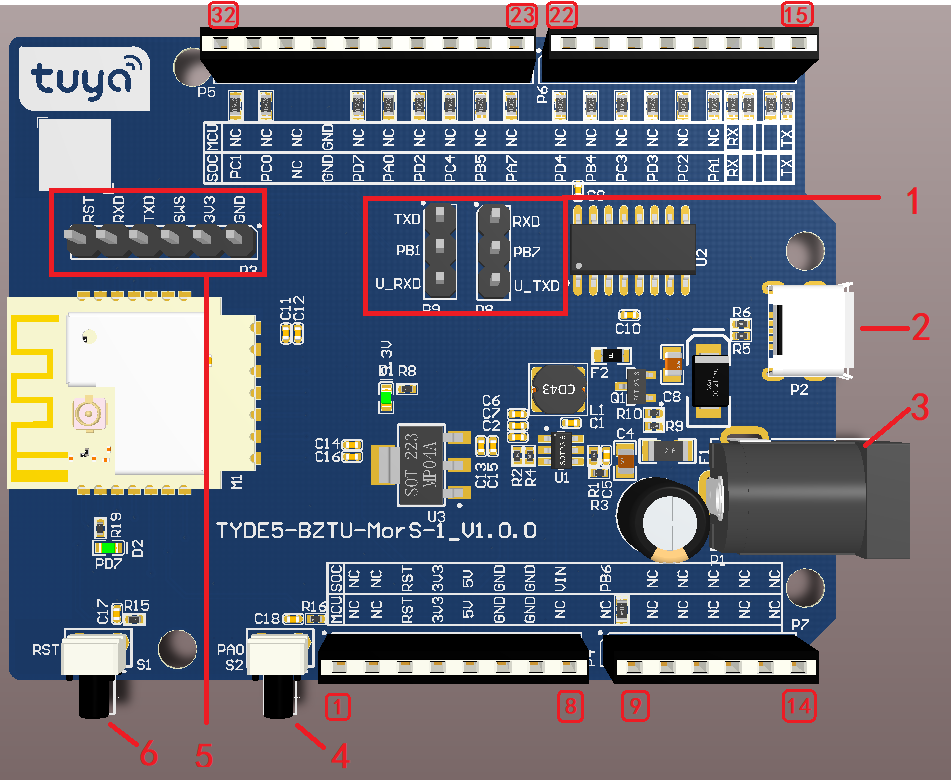
-
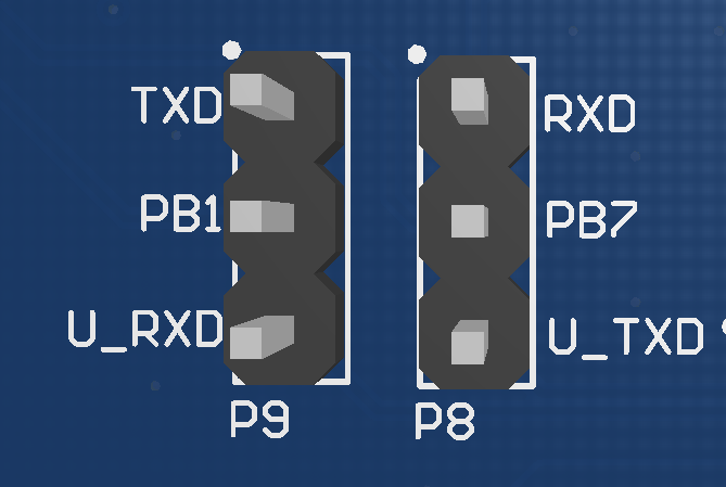
1: Jumper switches (P9 and P8), used to change the mode of the user port. Placing a jumper cap on
PB1-TXDandPB7-RXDenables the module’s pin to connect to the TX and RX pins. Placing a jumper cap onPB1-U_RXDandPB7-U_TXDenables the module’s pins to connect to the U2 chip so that the user port can communicate with the module through the micro-USB port. -
2: Micro-USB (P2): Inputs 5V DC voltage and provides one extended serial port.
-
3: DC-005 (P1): Inputs 12V DC voltage.
-
4: Button (S2): Connected to the
PA0pin on the module. When the button is pressed, the low level is output. When the button is released, the high level is output. -
5: Serial port (P3): Used to flash firmware to the ZTU module.
-
6: Button (S1): Connected to the
RSTpin on the module. When the button is pressed, the low level is output, and the module is reset. -
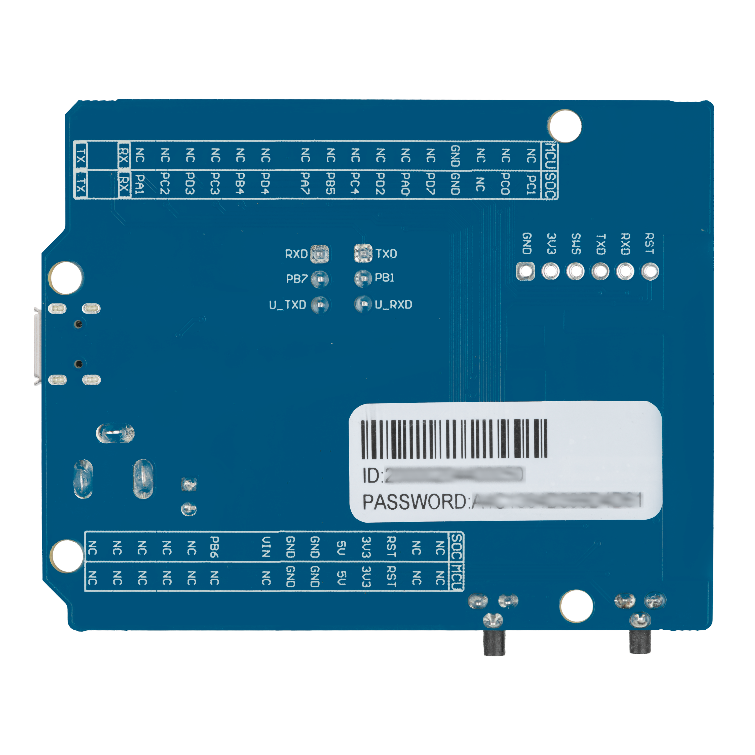
Pin description
No. Symbol Description 1 NC Leave it floating. 2 NC Leave it floating. 3 RST Reset the module, low-voltage reset. 4 3V3 3.3V power pin. 5 5V 5V power pin. 6 GND Ground pin. 7 GND Ground pin. 8 VIN 12V power pin. 9 PB6 GPIOB_6of the module, which can be reused as the ADC.10 NC Leave it floating. 11 NC Leave it floating. 12 NC Leave it floating. 13 NC Leave it floating. 14 NC Leave it floating. 15 TX Use a jumper cap to switch to the GPIOB_1pin of the module. This pin can be reused as the TXD of the user port.16 RX Use a jumper cap to switch to the GPIOB_7pin of the module. This pin can be reused as the RXD of the user port.17 PA1 GPIOA_1of the module.18 PC2 GPIOC_2of the module, which can be reused as the PWM.19 PD3 GPIOD_3of the module.20 PC3 GPIOC_3of the module, which can be reused as the PWM.21 PB4 GPIOB_4of the module, which can be reused as the PWM.22 PD4 GPIOD_4of the module.23 PA7 GPIOA_7of the module. It defaults to the SWS pin, used for firmware flashing.24 PB5 GPIOB_5of the module, which can be reused as the PWM.25 PC4 GPIOC_4of the module, which can be reused as the ADC.26 PD2 GPIOD_2of the module, which can be reused as the PWM.27 PA0 GPIOA_0of the module.28 PD7 GPIOD_7of the module.29 GND Ground pin. 30 NC Leave it floating. 31 PC0 GPIOC_0of the module.32 PC1 GPIOC_1of the module.
Load-carrying capacity
-
When DC-005 inputs 12V DC voltage, the board can supply power to external components.
Power pin Rated voltage/current VIN Depends on the input current of the adapter connected to the DC-005 terminal. 5V 5V/1A 3V3 3.3V/0.6A This board outputs rated power of 5W, which cannot support the long-time simultaneous output of 5V/1A and 3.3V/0.6A.
-
Characteristics of the output voltage of 5V
Output current 0A 0.25A 0.5A 0.75A 1A 1.25A Output voltage 5.01V 5.00V 4.99V 4.98V 4.98V 4.97V We tested the voltage under the condition that there is no output voltage on the 3V3 pin.
-
Characteristics of the output voltage of 3V3 pin
Output current 0A 0.15A 0.3A 0.45A 0.6A 0.75A Output voltage 3.34V 3.36V 3.37V 3.37V 3.38V 3.38V We tested the voltage under the condition that there is no output voltage on the 5V pin.
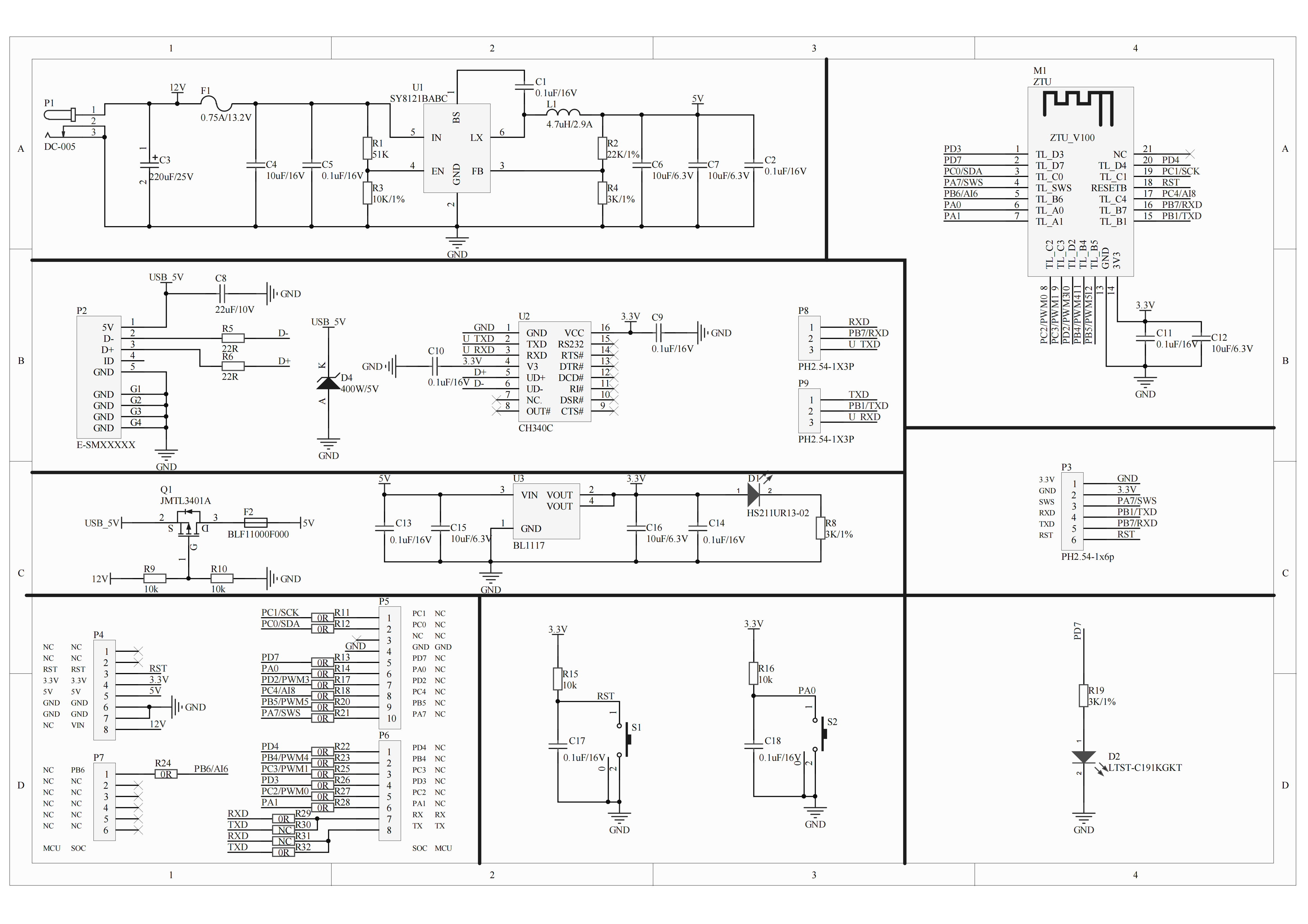
Schematic diagram and PCB
-
The schematic diagram of the board:
-
The PCB board:
How USB-to-serial works
-
The board has a built-in USB-to-serial chip. The single-channel USB port can provide one extended serial port. You can use a jumper cap to allow the user port on the module to connect to the USB-to-serial chip.
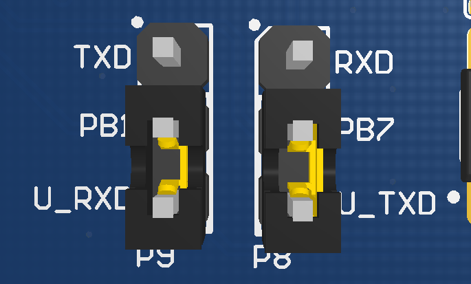
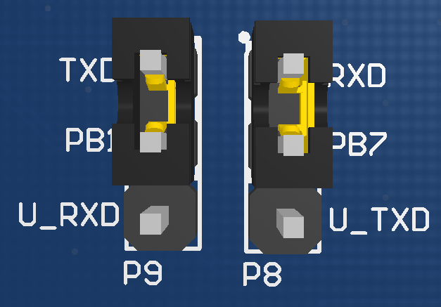
Pin connection description
Silkscreen P9 P8 Pins on module PB1 PB7 Pins on board TX RX USB-to-serial chip USB-RXD USB-TXD -
The serial port is left floating and not connected to the pins on the USB-to-serial chip or the board. The two headers are open without jumper caps.
-
The serial ports on the module are connected to the USB-to-serial chip. The TX and RX on the board are left floating. Put the jumper caps as shown below.
-
The serial ports on the module are connected to the pins on the board. The pins on the USB-to-serial chip are left floating. Put the jumper caps as shown below.
USB-to-serial chip driver
Download the USB-to-serial chip driver for your operating system.
Things to note
The board has a built-in power supply port and circuit, so the additional power board is not necessary.
Is this page helpful?
YesFeedbackIs this page helpful?
YesFeedback


