TYZS1 Module Datasheet
Last Updated on : 2024-11-20 08:22:20download
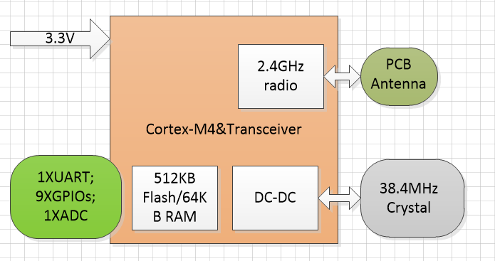
TYZS1 is a low-power embedded Zigbee module developed by Hangzhou Tuya Information Technology Co., Ltd. It consists of one EFR32MG13P632 highly integrated wireless RF processor chip and a small number of peripheral devices.
Product overview
It has a built-in 802.15.4 PHY/MAC Zigbee network protocol stack and rich library functions. The TYZS1 embeds a low-power 32-bit ARM Cortex-M4 core, 512KByte Flash program memory, 64KB RAM data memory, and a wealth of peripheral resources.
The TYZS1 is a FreeRTOS platform that gathers all Zigbee MAC and TCP/IP libraries into one place. It enables users to build on the product and develop embedded Zigbee products that suit their individual needs.
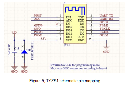
The TYZS1 schematic diagramas shown :
Features
A built-in low-power 32-bit ARM Cortex-M4 processor with a DSP instruction set and floating point unit that doubles as an application processor
- Supports main frequency of 40MHz
- Wide operating voltage: 1.8V-3.8V
- Peripherals: 9xGPIOs, 1xURT, 1xADC
- Zigbee operating characteristics
- Supports 802.15.4 MAC/PHY
- Operating channels 11 to 26 @2.400-2.483GHz and an air-interface rate of 250Kbps
- A built-in DC-DC circuit for maximum power efficiency
- +10dBm maximum output
- 63uA/MHz operating power consumption; 1.4uA sleep current
- Active net pairing with terminal devices
- Built-in onboard PCB antenna/reserved Ipex connector for high gain external antenna
- Operating temperature: -40℃ to 85℃
- Supports hardware encryption, supports AES 128/256
Primary application fields
- Smart buildings
- Smart homes/appliances
- Smart plugs, smart lighting
- Industrial wireless control
- Health and measurements
- Asset tracking
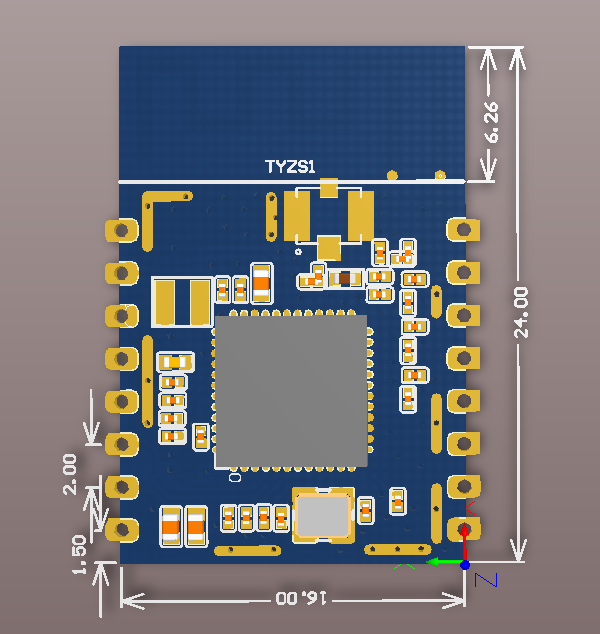
Module interfaces
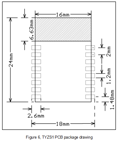
Package dimensions
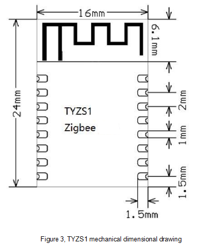
The TYZS1 has 2 rows of pins with a 2mm gap.
TYZS1 dimensions: 16mm (W) x 24mm (L) x 3.5mm (H). The TYZS1’s dimensions are shown in Figure 2:
Pin definition
Interface pins are defined as shown in Table 1:
Table 1, TYZS1 interface pins description
| Pin number | Symbol | IO type | Function |
|---|---|---|---|
| 1 | nRST | I | Hardware reset pin, the chip is reset when the pin is LOW; The module comes with a power-on reset and the user can use this pin as needed |
| 2 | ADC | AI | ADC port (1), 12-bit precision SAR analog-to-digital converter |
| 3 | NC | - | NC pin, external handling is not required |
| 4 | GPIO0 | I/O | GPIO pin usage. |
| 5 | SWO | I/O | GPIO pin usage/can be used as an output pin under JLINK communication. |
| 6 | PWM3 | I/O | GPIO pin usage. |
| 7 | PWM1 | I/O | GPIO pin usage. |
| 8 | VCC | P | Module power supply pin (common supply voltage : 3.3V) |
| 9 | GND | P | The reference ground of the module. |
| 10 | GPIO2 | I/O | GPIO pin usage. |
| 11 | SWDIO | I/O | JLINK SWDIO programming pin. Can be used as a GPIO pin in normal applications. |
| 12 | SWCLK | I/O | JLINK SWCLK programming pin. Can be used as a GPIO pin in normal applications. |
| 13 | PWM2 | I/O | GPIO pin usage. |
| 14 | GPIO3 | I/O | GPIO pin usage. |
| 15 | RXD | I/O | UART0_RXD |
| 16 | TXD | O | UART0_TXD |
Note: P indicates the power pin, I/O indicates the input/output pin, and AI indicates analog input pin.
RST is only the module hardware reset pin; it cannot clear Zigbee net-pairing information.
(1) : This pin can only be used as an ADC port. It cannot be used as a normal IO port. If it is not used, it needs to be left floating. As an ADC input, the input voltage range is limited to 0-AVDD and can be configured by software.
Test point definition
Test pins are defined in Table 2:
Table 2, TYZS1 test pins description
| Pin number | Symbol | IO Type | Function |
|---|---|---|---|
| - | - | I | For module production testing |
Description: This test pin is not recommended for use.
Electrical parameters
Absolute electrical parameters
Table 3, Absolute parameters
| Parameters | Description | Minimum value | Maximum value | Unit |
|---|---|---|---|---|
| Ts | Storage temperature | -50 | 150 | ℃ |
| VCC | Input voltage | -0.3 | 3.8 | V |
| Electrostatic discharge voltage (human-body model) | TAMB-25℃ | - | 2.5 | KV |
| Electrostatic discharge voltage (machine model) | TAMB-25℃ | - | 0.5 | KV |
Operating conditions
Table 4, Normal operating conditions
| Parameters | Description | Minimum value | Typical value | Maximum value | Unit |
|---|---|---|---|---|---|
| Ta | Operating temperature | -40 | - | 85 | ℃ |
| VCC | Operating voltage | 1.8 | 3.3 | 3.8 | V |
| VIL | IO low input | -0.3 | - | VCC*0.25 | V |
| VIH | IO high input | VCC*0.75 | - | VCC | V |
| VOL | IO low output | - | - | VCC*0.1 | V |
| VoH | IO high output | VCC*0.8 | - | VCC | V |
| Imax | IO drive current | - | - | 12 | mA |
Zigbee TX power consumption
Table 5, Power consumption during continuous TX
| Symbol | Rate | Transmission power | Typical value | Unit |
|---|---|---|---|---|
| IRF | 250Kbps | +10dBm | 32 | mA |
| IRF | 250Kbps | +4dBm | 17 | mA |
| IRF | 250Kbps | +1dBm | 11.8 | mA |
Note: When testing the above data, continuous transmission duty cycle=100%.
Zigbee RX power consumption
Table 6, RX continuous power
| Symbol | Rate | Typical value | Unit |
|---|---|---|---|
| IRF | 250Kbps | 8 | mA |
Note: When UART is active, the RX current is 14mA.
Power consumption when operating
Table 7, TYZS1 operating current
| Operation mode | Operating condition, Ta=25℃ | Average value | Maximum value | Unit |
|---|---|---|---|---|
| Quick configuration | Module in quick configuration state | 10 | 40 | mA |
| Network connection state | Connected to a network | 3 | 6 | mA |
| Deep sleep mode | Deep sleep mode and retains 64KB Flash | 3.5 | 5 | uA |
RF Characteristics
Basic RF characteristics
Table 8, Basic RF characteristics
| Operating frequency | Description |
|---|---|
| Operating frequency | 2.400 to 2.484GHz |
| Physical layer standard | IEEE 802.15.4 |
| Data transfer rate | 250Kbps |
| Antenna type | PCB antenna/Ipex connector external antenna |
| Line of sight | >120m |
Zigbee Output performance
Table 9, Continuous TX performance
| Parameter | Minimum value | Typical value | Maximum value | Unit |
|---|---|---|---|---|
| Maximum output | - | +10 | - | dBm |
| Minimum output | - | -30 | - | dBm |
| Output power adjustment step | - | 0.5 | 1 | dB |
| Frequency error | -15 | - | +15 | ppm |
| Output adjacent channel suppression | -31 | dBc |
Note: If extended coverage is required, consider our TYZS3 module as the interface is stronger.The TYZS1 through the wall.
Zigbee RX sensitivity
Table 10, RX Sensitivity
| Parameter | Minimum value | Typical value | Maximum value | Unit |
|---|---|---|---|---|
| PER<10%, RX sensitivity, 250Kbps@OQPSK | - | -102 | - | dBm |
Antenna signal
Antenna type
The default PCB onboard antenna access/reserved Ipex connector is used to extend the high gain external antenna in complex installation environments.
Antenna interference reduction
To optimize Zigbee performance of the wireless module in combination with the PCB onboard antenna, it is recommended to keep the antenna at least 15mm from other metal parts. It is recommended that the corresponding antenna area of the adapter board be hollowed out for the best effect.
The user PCB board should not be routed around the antenna area and should not be covered with copper to avoid affecting the antenna radiation performance. For the module PCB onboard antenna area, refer to Figure 3 below, “TYZS1 mechanical dimensional drawing”.
Packaging information and production guidance
Mechanical dimensions
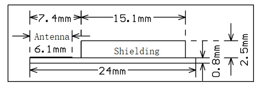
PCB recommended packaging
Production guide
-
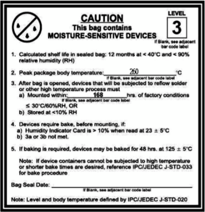
The stamp-hole module must be mounted by the SMT machine. After being unpacked, it must be soldered within 24 hours. Otherwise, it must be put into the drying cupboard where the RH is not greater than 10%, or it needs to be packaged under vacuum again and the exposure time needs to be recorded (the total exposure time cannot exceed 168 hours).
- SMT equipment:
- Mounter
- SPI
- Reflow soldering machine
- Oven temperature tester
- Automated optical inspection (AOI) equipment
- Baking equipment:
- Cabinet oven
- Anti-static heat-resistant pallets
- Anti-static heat-resistant gloves
- SMT equipment:
-
Storage conditions for a delivered module are as follows:
- The moisture-proof bag must be placed in an environment where the temperature is below 40°C and the relative humidity is lower than 90%.
- The shelf life of a dry-packaged product is 12 months from the date when the product is packaged and sealed.
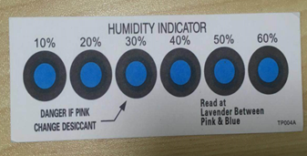
- The package contains a humidity indicator card (HIC).
-
The module needs to be baked in the following cases:
- Vacuum packing bag was found to be damaged before being unpacked.
- There is no humidity indicator card (HIC) in the vacuum packing bag.
- After being unpacked, 10% and above circles on the HIC become pink.
- The total exposure time has been more than 168 hours since unpacking.
- More than 12 months have passed since the sealing date of the bag.
-
Baking settings:
- Temperature: 60°C and ≤ 5%RH for reelizing and 125°C and ≤5%RH for palletizing (please use heat-resistant pallet rather than plastic pallet)
- Time: 48 hours for reelizing and 12 hours for palletizing
- Alarm temperature: 65°C for reelizing and 135°C for palletizing
- Production ready temperature after natural cooling: < 36°C
- The number of drying times: 1
- Re-baking condition: If a module remains unused for 168 hours after being unpacked, it must be baked again.
Important: If this batch of modules is not baked within 168 hours, do not use the wave soldering to solder them. Because these modules are 3-level moisture-sensitive components, they are very likely to get damp when exposed outside. In this case, if they are soldered at high temperatures, it may result in component failure or poor soldering.
-
In the whole production process, take electrostatic discharge (ESD) protective measures.
-
To guarantee the passing rate, it is recommended that you use the SPI and AOI to monitor the quality of solder paste printing and mounting.
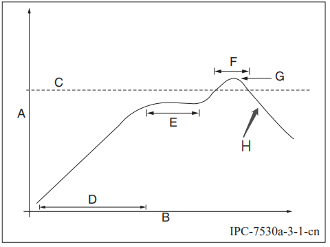
Recommended oven temperature curve
Perform mounting with the SMT based on the following reflow oven temperature curve. The highest temperature is 245°C. The reflow temperature curve is as below:
-
A: Temperature axis
-
B: Time axis
-
C: Liquidus temperature: 217 to 220°C
-
D: Ramp-up slope: 1 to 3°C/s
-
E: Duration of constant temperature: 60 to 120s; the range of constant temperature: 150 to 200°C
-
F: Duration above the liquidus: 50 to 70s
-
G: Peak temperature: 235 to 245°C
-
H: Ramp-down slope: 1 to 4°C/s
Note: The above curve is just an example of the solder paste SAC305. For more details about other solder pastes, please refer to Recommended oven temperature curve in the solder paste specifications.
Storage conditions
Is this page helpful?
YesFeedbackIs this page helpful?
YesFeedback


