Wi-Fi and Bluetooth Low Energy Combo Core Board (BK7252)
Tuya Sandwich Wi-Fi and Bluetooth Low Energy (LE) combo core board is designed for audio and video applications. It contains a rich set of peripherals, such as I2C, SPI, PWM, ADC, and SD card interface. You can connect to a range of external peripheral devices or Tuya Sandwich series boards.
Scenarios
The hardware on this TYDE5-BK7252-Core-1 (BK7252) core board can automatically output the captured images in JPEG. The built-in high-performance audio ADC and audio DAC are used for audio capture and playback.
-
This board applies to a wide range of use cases such as smart access control systems, lockers, welcome greeting doorbells, text-to-speech readers, pet feeders, door locks, and camera doorbells.
-
It can work with a GC0328 camera module to help you build image recognition solutions. Backed by the Tuya Developer Platform, you can perform custom development such as QR code scanner.
-
You can use this board for different development purposes.
-
Embedded program development and debugging
-
App development and debugging
-
Creating connected devices that can be controlled with a mobile phone
-
Getting started with IoT development and diving into the Wi-Fi-based control system, image recognition, and audio and video transmission
-
Components
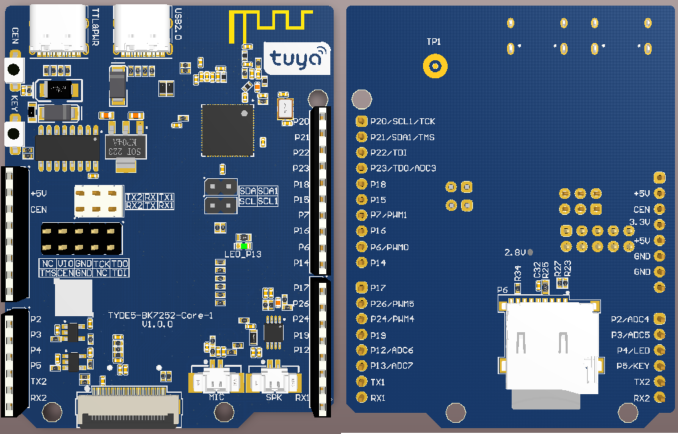
Tuya Sandwich Wi-Fi and Bluetooth LE combo core board is based on the BEKEN’ BK7252 Wi-Fi and Bluetooth LE combo chip. It consists of CS8302M audio amplifier, two USB-C ports, CH340C USB-to-TTL chip, flip FPC connector, buttons, indicators, and other components.
I/O port functions
-
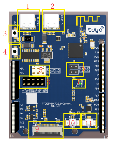
1: TTL & PWR: Provides 5V DC voltage and one extended serial port.
-
2: USB 2.0: Full-speed USB 2.0 port.
-
3: Button (CEN): When the button is pressed, the chip is reset.
-
4: Button (KEY): When the button is pressed, P5 outputs low. When the button is released, it outputs high.
-
5: Jumper (TTL to UART1/UART2): Connect TTL & PWR to UART1 or UART2 using a jumper cap.
-
6: Jumper (I2C): Connect the I2C1 on BK7252 to the I2C on the FPC connector, or disconnect them.
-
7: LED indicator: When P4 outputs low, the LED is on.
-
8: JTAG port: Compatible with the HW SPI port on the flashing tool from the chip manufacturer, used to download the program to the chip.
-
9: FPC connector: Compatible with the GC0328 and GC2145 CMOS camera modules.
-
10: MIC: 1.25 mm 2-pin microphone connector.
-
11: SPK: 1.25 mm 2-pin speaker connector, which can be connected to 8Ω 2W or 4Ω 3W speakers.
-
Pin description
No. Symbol Description 1 NC Leave it floating. 2 +5V 5V power pin. 3 CEN Clock enable (CEN) pin on BK7252. It can output the chip enable and high enable signals. 4 3.3V 3.3V power pin. 5 +5V 5V power pin. 6 GND Ground pin. 7 GND Ground pin. 8 NC Leave it floating. 9 P2 GPIOP_2 on BK7252, which can be reused as the ADC. 10 P3 GPIOP_3 on BK7252, which can be reused as the ADC. 11 P4 GPIOP_4 on BK7252, which can be reused as the LED pin. 12 P5 GPIOP_5 on BK7252, which can be reused as the button pin. 13 P0 GPIOP_0 on BK7252, which can be reused as the UART2 TXD pin, generally used for log printing. 14 P1 GPIOP_1 on BK7252, which can be reused as the UART2 RXD pin, generally used for log printing. 15 P10 GPIOP_10 on BK7252, which can be reused as the UART1 RXD pin and generally used as the user I/O. 16 P11 GPIOP_11 on BK7252, which can be reused as the UART1 TXD pin and generally used as the user I/O. 17 P13 GPIOP_13 on BK7252, which can be reused as the ADC. 18 P12 GPIOP_12 on BK7252, which can be reused as the ADC. 19 P19 GPIOP_19 on BK7252, which can be reused as the SD_D1. 20 P24 GPIOP_24 on BK7252. 21 P26 GPIOP_26 on BK7252. 22 P17 GPIOP_17 on BK7252, which can be reused as the SD_D0. 23 P14 GPIOP_14 on BK7252, which can be reused as the SD_CLK. 24 P6 GPIOP_6 on BK7252, which can be reused as the PWM0. 25 P16 GPIOP_16 on BK7252, which can be reused as the SD_CMD. 26 P7 GPIOP_7 on BK7252, which can be reused as the PWM1. 27 P15 GPIOP_15 on BK7252, which can be reused as the SD_D3. 28 P18 GPIOP_18 on BK7252, which can be reused as the SD_D2. 29 P23 GPIOP_23 on BK7252, which can be reused as the ADC and JTAG_TDO. 30 P22 GPIOP_22 on BK7252, which can be reused as the JTAG_TDI. 31 P21 GPIOP_21 on BK7252, which can be reused as the SDA and JTAG_TMS of the I2C1. 32 P20 GPIOP_20 on BK7252, which can be reused as the SCL and JTAG_TCK of the I2C1.
Load-carrying capacity
-
When TTL & PWR inputs 5V DC voltage, the board can supply power to external components.
Power pin Rated voltage/current 5V Depends on the input current of the adapter connected to the DC-005 terminal. The maximum output current flowing through the resettable fuse is 1A. 3.3V 3.3V/1.0A -
Characteristics of output voltage
Output current 0A 0.15A 0.3A 0.45A 0.6A 0.75A Output voltage 3.29V 3.28V 3.06V 2.95V 2.82V 2.69V
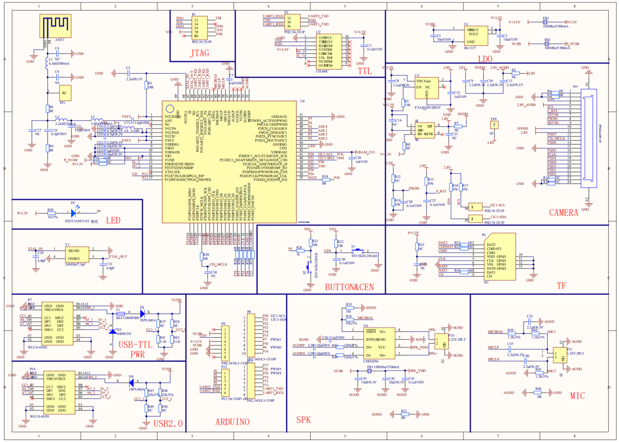
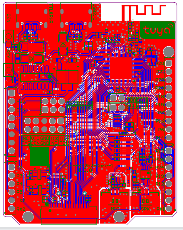
Schematic diagram and PCB
-
The schematic diagram of the board:
-
The PCB board:
How USB-to-TTL works
-
The board has a built-in USB-to-TTL chip. The single-channel USB port can provide one extended serial port. You can use a jumper cap to allow the 2-channel serial port on the chip to connect to the USB-to-TTL chip. Pin connection description
CH340C BK7252_UART1 BK7252_UART2 Silkscreen markings RX TX1 TX2 TX RX1 RX2 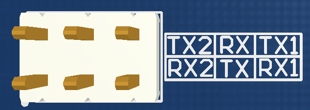
-
The serial port on BK7252 is left floating and not connected to the pins on the USB-to-TTL chip or the core board. The six headers are open without jumper caps.
-
To connect the UART 1 on the BK7252 to the USB-to-TTL chip, connect RX to TX1 and TX to RX1 by using jumper caps.
-
To connect the UART 2 on the BK7252 to the USB-to-TTL chip, connect RX to TX2 and TX to RX2 by using jumper caps.
-
The USB-to-TTL chip cannot connect to UART 1 and UART 2 at the same time.
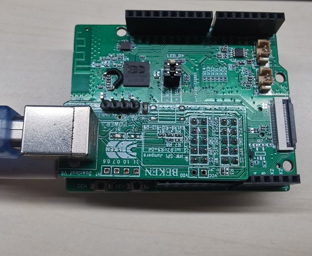
Connection for flashing
For flashing license and firmware, connect pins following the table and figure shown below.
| Pins on core board | Pins on flashing tool | Flashing tool |
|---|---|---|
| TX1 | USB-RX (with a jumper cap) | Connect to TTL & PWR with a USB Type-C cable |
| RX1 | USB-TX (with a jumper cap) | |
| GND | GND | |
| TDO | MISO | HW SPI on the flashing tool from the chip manufacturer |
| TDI | MISI | |
| TCK | P2.3 | |
| GND | GND | |
| VIO | 3.3V | |
| CEN | VPP | |
| TMS | CS |
If the chip has a bootloader installed, you can directly use the UART 1 to flash firmware and license. Generally, the chip comes with a bootloader.
USB-to-TTL chip driver
Download the USB-to-TTL chip driver for your operating system.
Things to note
-
The board has a built-in power supply port and circuit, so the additional power board is not necessary.
-
This board contains a reserved TF card interface. You can solder the TF card components on the other side of the board if needed. The reused GPIO only works to drive the TF card.
-
This board is compatible with the GC0328 and GC2145 CMOS camera modules. If you choose the GC2145 camera, you need to solder the LDO SMB130F18-C5TR (U5), peripherals, and R2 in order to start the GC2145 camera.
Is this page helpful?
YesFeedbackIs this page helpful?
YesFeedback


