Wi-Fi and Bluetooth Low Energy Combo Core Board (BK7256)
Tuya Sandwich Wi-Fi and Bluetooth Low Energy (LE) combo core board is designed for audio and video applications. It contains a rich set of peripherals, such as UART, I2C, SPI, PWM, LCD interface (8080 or RGB565), and SD card interface. You can connect to a range of external peripheral devices or Tuya Sandwich series boards.
Scenarios
-
The hardware on this TYDE5-BK7256-Core-1 (BK7256) core board can automatically output the captured images in JPEG. The built-in high-performance audio ADC and audio DAC are used for audio capture and playback.
-
This board applies to a wide range of use cases such as smart access control systems, lockers, welcome greeting doorbells, text-to-speech readers, pet feeders, door locks, and camera doorbells.
-
It can work with a GC0328 or GC2145 camera module to help you build image recognition solutions. Backed by the Tuya Developer Platform, you can perform custom development.
-
You can use this board for different development purposes.
-
Embedded program development and debugging
-
App development and debugging
-
Creating connected devices that can be controlled with a mobile phone
-
Getting started with IoT development and diving into the Wi-Fi-based control system, image recognition, and audio and video transmission.
-
Components
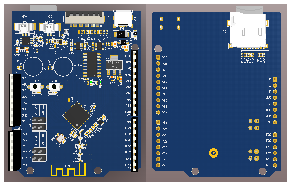
The core board is integrated with the cost-effective Wi-Fi 6 and Bluetooth LE combo chip BK7256 from Beken Corporation. It consists of CS8302M audio amplifier, micro-USB socket, CH340C USB-to-TTL chip, flip FPC connector, buttons, indicators, and other components.
I/O port functions
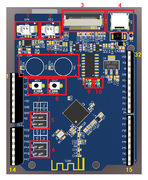
- SPK: 1.25 mm 2-pin speaker connector, which can be connected to 8Ω 2W or 4Ω 3W speakers.
- MIC: 1.25 mm 2-pin microphone connector.
- FPC connector: Compatible with the GC0328 and GC2145 CMOS camera modules.
- P7: Provides 5V DC voltage and one extended serial port.
- Jumper (USB-to-TTL): Set the jumper on P8 and P11 to select the USB port.
- Jumper (I2C): Set the jumper on P1 and P2 to disconnect or connect the I2C of the BK7256 chip to the I2C of the FPC connector.
- Button (KEY): When P9 outputs low, the button is active.
- Button (RST): When the button is pressed, the chip is reset.
- LED (D2): When P6 outputs high, the LED is on.
- LED (D1): Indicates the power status of the system.
- Touch key: P13 detects the TP1. P12 detects the TP2.
Pin description
| No. | Pin | Description |
|---|---|---|
| 1 | NC | Leave it floating. |
| 2 | +5V | 5V power pin. |
| 3 | NC | Leave it floating. |
| 4 | 3.3V | 3.3V power pin. |
| 5 | +5V | 5V power pin. |
| 6 | GND | Ground pin. |
| 7 | GND | Ground pin. |
| 8 | NC | Leave it floating. |
| 9 | P23 | GPIOP_23 on BK7256. It can be reused as the DL_SO (SPI flash download), ADC3, QSPI (CSN), and LCD (RGB11). |
| 10 | P22 | GPIOP_22 on BK7256. It can be reused as the DL_SI (SPI flash download), CLK26M (26 MHz clock output), ADC5, QSPI (CLK), and LCD (RGB12). |
| 11 | P45 | GPIOP_45 on BK7256. It can be reused as the CAN (RX), SPI1 (CSN), ADC11, and LCD (RGB2). |
| 12 | P44 | GPIOP_44 on BK7256. It can be reused as the CAN (TX), SPI1 (SCK), ADC10, and LCD (RGB3). |
| 13 | P43 | GPIOP_43 on BK7256. It can be reused as the I2C2 (SDA), I2S (DOUT), and LCD (RGB4). |
| 14 | P42 | GPIOP_42 on BK7256. It can be reused as the I2C2 (SCL), I2S (DIN), and LCD (RGB5). |
| 15 | P40 | GPIOP_40 on BK7256. It can be reused as the UART3 (RX), I2S (CLK), and LCD (RGB7). |
| 16 | P41 | GPIOP_41 on BK7256. It can be reused as the UART3 (TX), I2S (SYNC), and LCD (RGB6). |
| 17 | P47 | GPIOP_47 on BK7256. It can be reused as the SPI1 (MISO), Touch Sensor 15, and LCD (RGB0). |
| 18 | P46 | GPIOP_46 on BK7256. It can be reused as the CAN STB (active high), SPI1 (MOSI), Touch Sensor 14, and LCD (RGB1). |
| 19 | P28 | GPIOP_28 on BK7256. It can be reused as the RXEN (it is high when Wi-Fi RF is receiving), I2S (MCLK), ADC4, and Touch Sensor 2. |
| 20 | P25 | GPIOP_25 on BK7256. It can be reused as the IrDA (TX/RX), PWM5, ADC1, QSPI (IO1), and LCD (RGB9). |
| 21 | P24 | GPIOP_24 on BK7256. It can be reused as the CLK32K (32 kHz clock output), PWM4, ADC2, QSPI (IO0), and LCD (RGB10). |
| 22 | P18 | GPIOP_18 on BK7256. It can be reused as the SD (D2) and LCD (RGB16). |
| 23 | P26 | GPIOP_26 on BK7256. It can be reused as the TXEN (it is high when Wi-Fi RF is transmitting), QSPI (IO2), and LCD (RGB8). |
| 24 | P19 | GPIOP_19 on BK7256. It can be reused as the SD (D3) and LCD (RGB15). |
| 25 | P15 | GPIOP_15 on BK7256. It can be reused as the SD (CMD), SPI1 (CSN), BT Antenna Selection 1, and LCD (RGB19). |
| 26 | P16 | GPIOP_16 on BK7256. It can be reused as the SD (D0), SPI1 (MOSI), BT Antenna Selection 2, and LCD (RGB18). |
| 27 | P17 | GPIOP_17 on BK7256. It can be reused as the SD (D1), SPI1 (MISO), BT Antenna Selection 3, and LCD (RGB17). |
| 28 | P14 | GPIOP_14 on BK7256. It can be reused as the SD (CLK), SPI1 (SCK), BT Antenna Selection 0, and LCD (RGB20). |
| 29 | GND | Ground pin. |
| 30 | NC | Leave it floating. |
| 31 | P21 | GPIOP_21 on BK7256. It can be reused as the DL_SCK (SPI flash download), I2C1 (SDA), SWDIO (SWD data), ADC6, and LCD (RGB13). |
| 32 | P20 | GPIOP_20 on BK7256. It can be reused as the DL_CSN (SPI flash download), I2C1 (SCL), SWCLK (SWD clock), and LCD (RGB14). |
Load-carrying capacity
When micro-USB (P7) inputs 5V DC voltage, the board can supply power to external components.
| Power pin | Rated voltage/current |
|---|---|
| 5V | Depends on the input current of the adapter connected to the micro-USB (P7) terminal. |
| 3.3V | 3.3V/0.6A |
Characteristics of output voltage
| Output current | 0A | 0.15A | 0.3A | 0.45A | 0.6A | 0.75A |
|---|---|---|---|---|---|---|
| Output voltage | 3.34V | 3.36V | 3.37V | 3.37V | 3.38V | 3.38V |
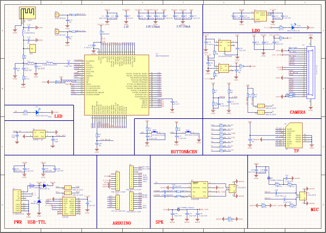
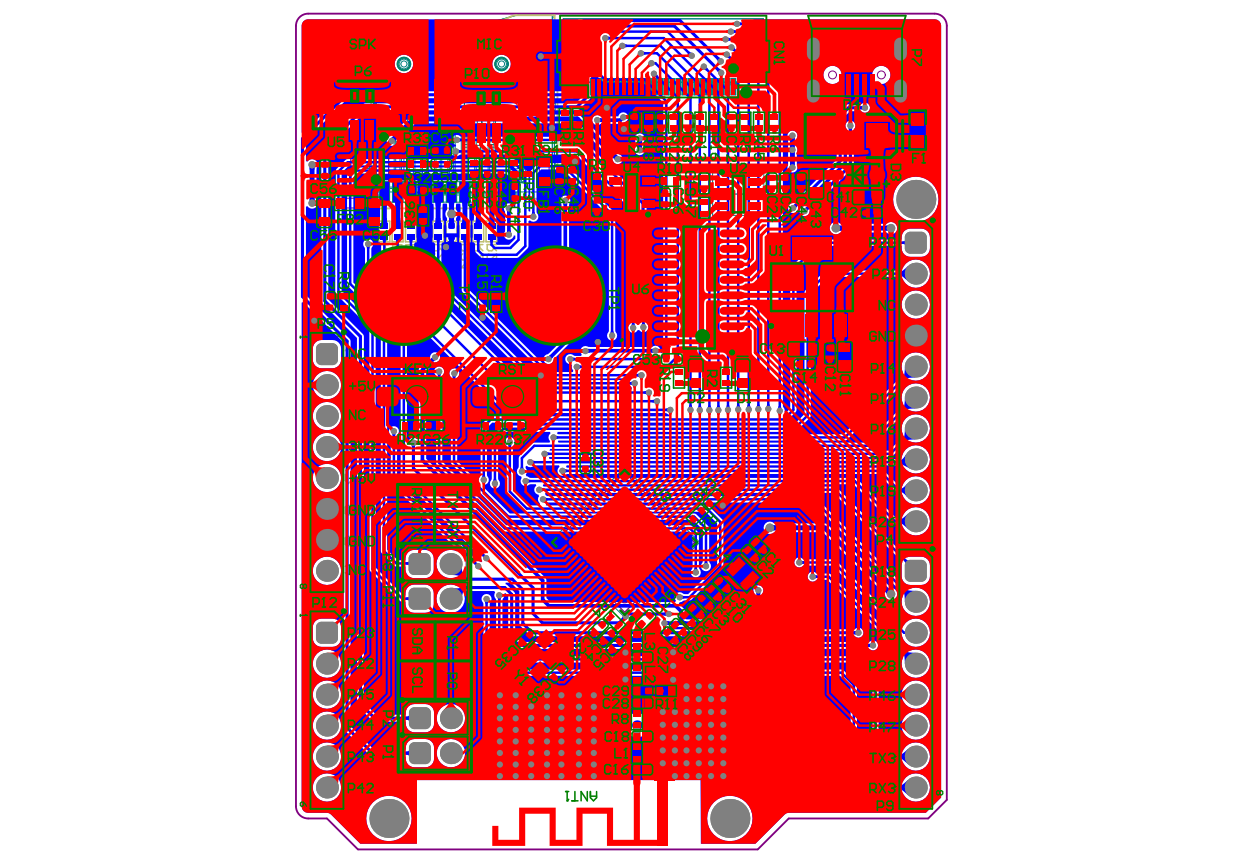
Schematic diagram and PCB
-
The schematic diagram of the board:
-
The PCB board:
How USB-to-TTL works
The board has a built-in USB-to-TTL chip. You can set the jumper to connect UART1 to the USB-to-TTL chip.
Pin connection description
| USB-to-serial chip | UART1 | |
|---|---|---|
| Silkscreen markings | RX | TX1(P11) |
| TX | RX1(P10) |
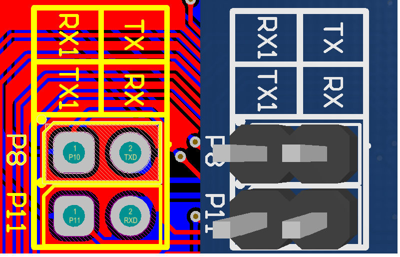
To connect the UART 1 on the BK7256 to the USB-to-TTL chip, connect RX to TX1 and TX to RX1 by using jumper caps.
Connection for DOWNLOAD mode
Download programs to the chip via the USB port (UART1). For flashing license and firmware, connect pins following the table and figure shown below.
| Pins on core board | Pins on flashing tool | Flashing tool |
|---|---|---|
| TX1 | USB-RX (with a jumper cap) | Connect the micro-USB cable to P7 |
| RX1 | USB-TX (with a jumper cap) | |
| 3.3V | 3.3V | |
| GND | GND | |
Things to note
-
The board has a built-in power supply port and circuit, so the additional power board is not necessary.
-
This board supports a 5V power supply from the USB port.
-
This board contains a reserved TF card interface. You can solder the TF card components on the other side of the board as well as seven resistors, namely R20, R23, R24, R26, R27, R28, and R29.
-
This board is compatible with the GC0328 and GC2145 CMOS camera modules. If you use a GC2145 camera module, solder the power supply IC
U4and then solder the capacitors and resistors (C26, R10, C30, and R9) that are close to theU4pin. If you use a GC0328 camera module, this soldering is not required. U4 is a voltage regulator IC, with a 1.8V voltage output. -
When you solder the camera socket, make sure the wiring of the socket and camera module is matched against the schematic diagram. Otherwise, the camera cannot work.
Is this page helpful?
YesFeedbackIs this page helpful?
YesFeedback


