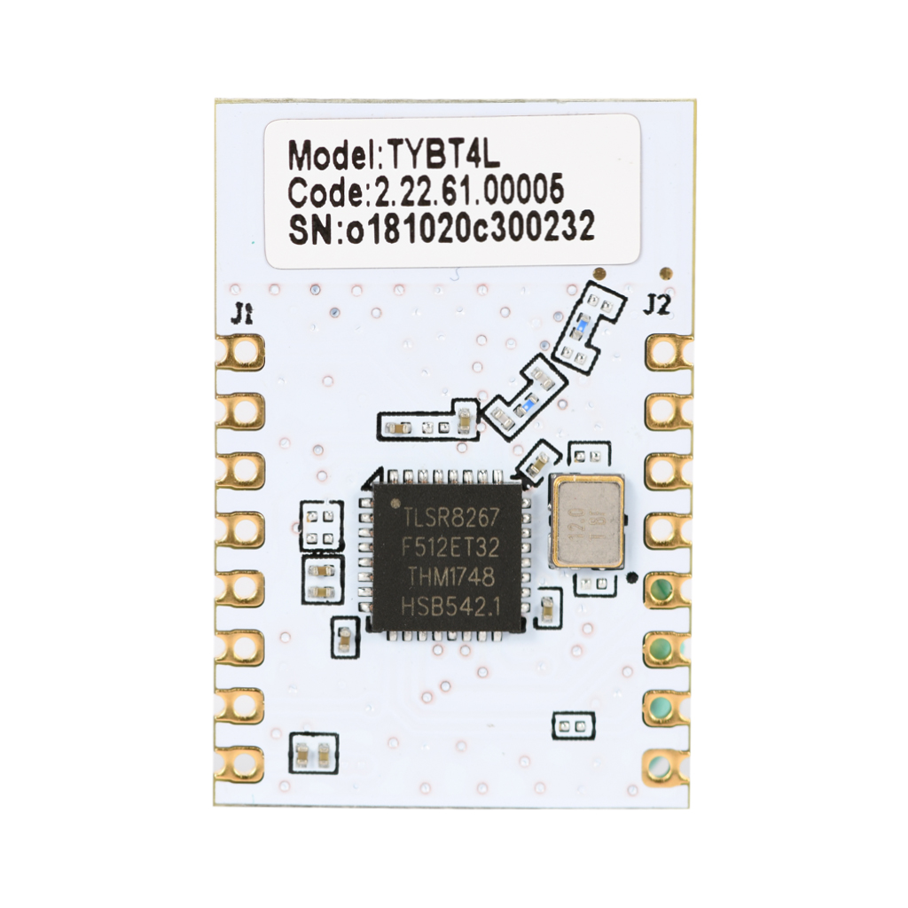
TYBT4L Module Datasheet
TYBT4L is a low power-consuming built-in Bluetooth module developed by Hangzhou Tuya Information Technology Co., Ltd. It consists of a highly integrated Bluetooth chip (TLSR8269) and several peripheral electrical circuits, with a built-in Bluetooth network communication protocol stack and robust library functions.
Overview
TYBT4L contains a low power-consuming 32-bit MCU, a Bluetooth 2.4 GHz radio, a 512 KB flash, a 16 KB SRAM, and nine multiplex I/O ports.
Features
- Built-in low power-consuming 32-bit CPU, which can also be used as an application processor
- Basic frequency: 48 MHz supported
- Working voltage:1.9 V to 3.6 V
- Peripherals: one I2C interface, five PWMs, and one UART
- Bluetooth RF features
- Compatible with Bluetooth 4.2
- RF data rate: up to 2 Mbit/s
- TX power: +7 dBm
- RX sensitivity: –92 dBm
- Built-in AES encryption for hardware
- Onboard PCB antenna
- Working temperature: –20°C to +105°C
Major application fields
- Intelligent LED
- Intelligent home
- Industrial low-power sensor
Module interfaces
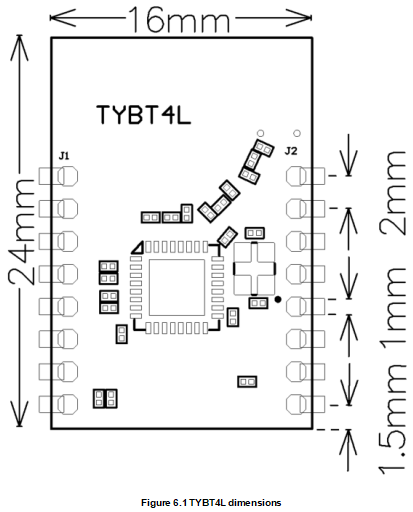
Dimensions and footprint
TYBT4L provides two rows of pins with a distance of 2.0 mm between every two pins.
TYBT4L dimensions: 16 mm (W) x 24 mm (L) (see figure 2.1)
Pin Definition
Table 2.1 describes the interface pins.
Table 2.1 TYBT4L interface pins
| No. | Symbol | I/O Type | Functions |
|---|---|---|---|
| 1 | RST | I | Module reset pin |
| 2 | ADC | I | External analog input |
| 3 | NC | / | NC interface, which is not connected |
| 4 | SDA | I/O | Pin for the data line of the I2C interface, which must be connected to a 4.7 kΩ pull-up resistor. This pin can also be used as the common I/O interface. |
| 5 | B | I/O | Common I/O interface, which can be used for PWM output of the LED driver. It controls the blue LED by default. |
| 6 | G | I/O | Common I/O interface, which can be used for PWM output of the LED driver. It controls the green LED by default. |
| 7 | WW | I/O | Common I/O interface, which can be used for PWM output of the LED driver. It controls the warm white LED by default. |
| 8 | 3.3 V | P | Module power supply input pin |
| 9 | GND | P | Module power supply reference ground pin |
| 10 | PA7 | I/O | Used as the common I/O interface |
| 11 | SWS | I/O | Bluetooth chip programming pin |
| 12 | SCL | I/O | Pin for the clock line of the I2C interface, which must be connected to a 4.7 kΩ pull-up resistor. This pin can also be used as the common I/O interface. |
| 13 | R | I/O | Common I/O interface, which can be used for PWM output of the LED driver. It controls the red LED by default. |
| 14 | CW | I/O | Common I/O interface, which can be used for PWM output of the LED driver. It controls the cold white LED by default. |
| 15 | RX | I/O | Serial port TX pin, used as the common I/O interface |
| 16 | TX | I/O | Serial port TX pin, used as the common I/O interface |
Note: P indicates power-supply pins and I/O indicates input/output pins.
- The SWS pin is used only for the programming of module firmware.
- The I2C pin does not provide a pull-up resistor. It must be connected to an external pull-up resistor.
- When the WW pin is used for PWM output, its polarity is opposite to that of the R, G, B, and CW pins used for PWM output.
- If you have special requirements for the light color controlled by PWM output, contact our business manager.
Electrical characteristics
Absolute electrical characteristics
Table 3.1 Absolute electrical characteristics
| Parameters | Description | Minimum value | Maximum value | Unit |
|---|---|---|---|---|
| Ts | Storage temperature | -40 | 125 | ℃ |
| VCC | Power supply voltage | -0.3 | 3.9 | V |
| Static electricity voltage (human model) | TAMB-25℃ | - | 2 | KV |
| Static electricity voltage (machine model) | TAMB-25℃ | - | 0.5 | KV |
Electrical conditions
Table 3.2 Normal electrical conditions
| Parameter | Description | Minimum Value | Typical Value | Maximum Value | Unit |
|---|---|---|---|---|---|
| Ta | Working temperature | -20 | - | 105 | °C |
| VCC | Working voltage | 1.9 | 3.3 | 3.6 | V |
| VIL | I/O low-level input | -0.3 | - | VCC*0.3 | V |
| VIH | I/O high-level input | VCC*0.7 | - | VCC | V |
| VOL | I/O low-level output | VSS | - | 0.3 | V |
| VoH | I/O high-level output | VCC-0.3 | - | VCC | V |
Power consumption in operating mode
Table 3.3 TX power consumption during constant emission
| Symbol | Condition | Typical Value | Unit |
|---|---|---|---|
| Itx | Constant emission, with 0 dBm output power | 15 | mA |
| Irx | Constant receiving | 12 | mA |
| IDC | Mesh connected | 27 | mA |
| Ideepsleep | Sleep mode | 18 | μA |
RF features
Basic RF features
Table 4.1, Basic RF features
| Parameter | Description |
|---|---|
| Frequency band | 2.4 GHz ISM band |
| Radio standard | Bluetooth 4.2 |
| Data transmitting rate | 1 Mbps |
| Antenna type | Onboard PCB antenna |
RF Output Power
Table 4.2 TX power during constant emission
| Parameter | Minimum Value | Typical Value | Maximum Value | Unit |
|---|---|---|---|---|
| RF average output power | 3.8 | 7 | 8 | dBm |
| 20 dB bandwidth (1 M) | - | 1300 | - | KHz |
RF RX sensitivity
Table 4.3 RX sensitivity
| Parameter | Rate | Minimum Value | Typical Value | Maximum Value | Unit |
|---|---|---|---|---|---|
| RX sensitivity | 1Mbps | –93 | –92 | –90 | dBm |
| Frequency offset error | 1Mbps | –300 | - | +300 | kHz |
| Co-channel interference suppression | - | - | –7 | - | dB |
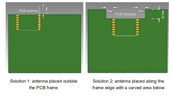
Antenna Information
Antenna types
TYBT4L uses the onboard MIFA antenna working in the 2.4 GHz Wi-Fi band for the PCB.
Antenna interference reduction
To ensure optimal RF performance, it is recommended that there be a space of at least 15 mm between the module antenna and other metal parts.
TYBT4L is attached to the PCB with other components using the SMT. In this case, the routing position and method of the PCB antenna directly affect the RF performance. The following figures show the recommended and not recommended routing positions.
-
As shown in Figure 5.1, if most of the antenna is outside the PCB frame, solutions 1 and 2 are recommended. The antenna is placed outside the PCB frame or the PCB is carved to reserve an area for the antenna. By using these two solutions, the performance of TYBT4L is almost the same as that of the module when being tested independently.
-
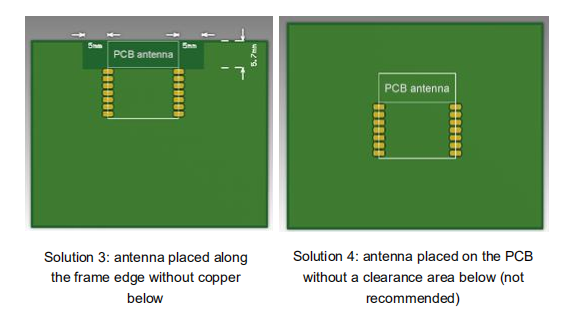
If the antenna must be routed on the PCB due to restrictions, solution 3 is recommended. The antenna is placed inside the PCB frame and no copper or wire is routed near the antenna. If this solution is used, the performance is reduced by about 1–2 dBm.
-
It is not recommended that solution 4 be used, in which the antenna is placed inside the PCB, and copper and other wires are routed under the antenna. In this solution, the RF signal has significant attenuation.
Packaging information and production instructions
Mechanical dimensions and size of the back pad
Production instructions
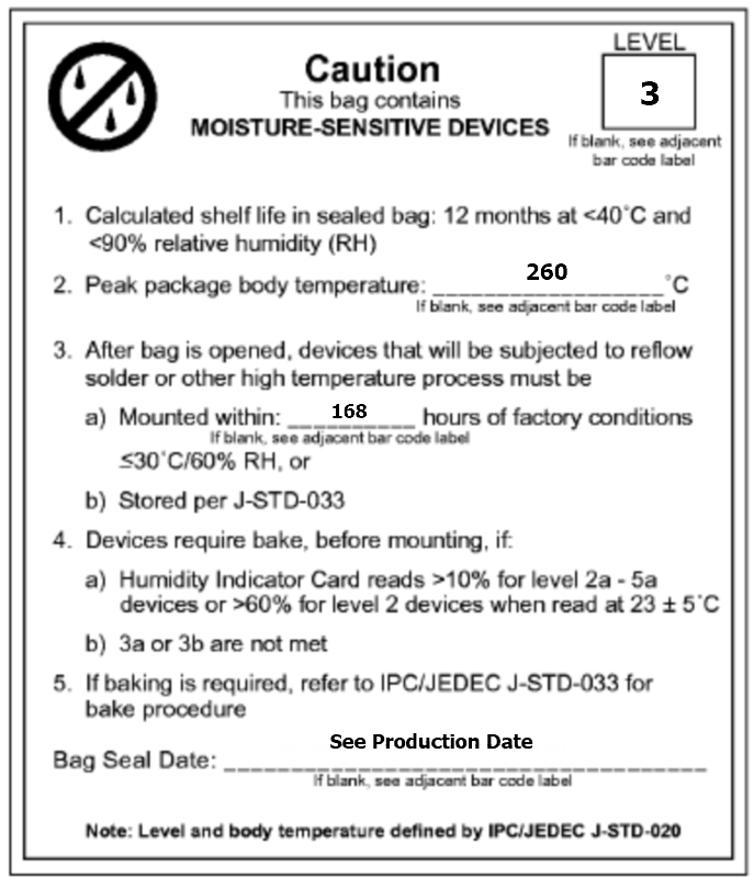
- The Tuya SMT module should be mounted by the SMT device. After being unpacked, it should be soldered within 24 hours. Otherwise, it should be put into the drying cupboard where the RH is not greater than 10%; or it needs to be packaged under vacuum again and the exposure time needs to be recorded (the total exposure time cannot exceed 168 hours).
- SMT devices:
- Mounter
- SPI
- Reflow soldering machine
- Thermal profiler
- Automated optical inspection (AOI) equipment
- Baking devices:
- Cabinet oven
- Anti-electrostatic and heat-resistant trays
- Anti-electrostatic and heat-resistant gloves
- SMT devices:
- Storage conditions for a delivered module:
-
The moisture-proof bag must be placed in an environment where the temperature is below 40°C and the relative humidity is lower than 90%.
-
The shelf life of a dry-packaged product is 12 months from the date when the product is packaged and sealed.
-
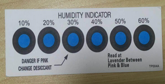
There is a humidity indicator card (HIC) in the packaging bag.
-
- The module needs to be baked in the following cases:
- The packaging bag is damaged before unpacking.
- There is no HIC in the packaging bag.
- After unpacking, circles of 10% and above on the HIC become pink.
- The total exposure time has lasted for over 168 hours since unpacking.
- More than 12 months have passed since the sealing of the bag.
- Baking settings:
- Temperature: 40°C and ≤ 5% RH for reel package and 125°C and ≤5% RH for tray package (please use the heat-resistant tray rather than plastic container)
- Time: 168 hours for reel package and 12 hours for tray package
- Alarm temperature: 50°C for reel package and 135°C for tray package
- Production-ready temperature after natural cooling: < 36°C
- Re-baking situation: If a module remains unused for over 168 hours after being baked, it needs to be baked again.
- If a batch of modules is not baked within 168 hours, do not use the reflow soldering to solder them. Because these modules are Level-3 moisture-sensitive devices, they are very likely to get damp when exposed beyond the allowable time. In this case, if they are soldered at high temperatures, it may result in device failure or poor soldering.
- In the whole production process, take electrostatic discharge (ESD) protective measures.
- To guarantee the passing rate, it is recommended that you use the SPI and AOI to monitor the quality of solder paste printing and mounting.
Recommended oven temperature curve
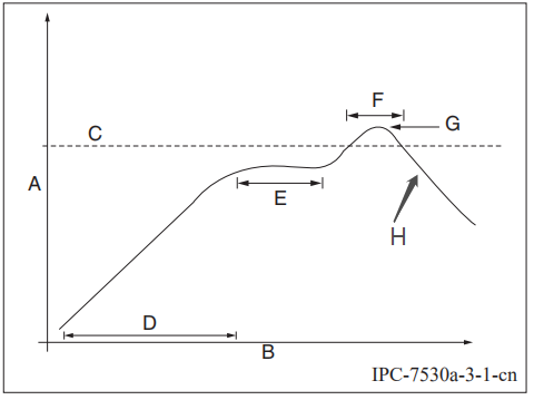
Set oven temperatures according to the following temperature curve of reflow soldering. The peak temperature is 245°C.
-
A: Temperature axis
-
B: Time axis
-
C: Liquidus temperature: 217 to 220°C
-
D: Ramp-up slope: 1 to 3°C/s
-
E: Duration of constant temperature: 60 to 120s; the range of constant temperature: 150 to 200°C
-
F: Duration above the liquidus: 50 to 70s
-
G: Peak temperature: 235 to 245°C
-
H: Ramp-down slope: 1 to 4°C/s
Note: The above curve is just an example of the solder paste SAC305. For more details about other solder pastes, please refer to Recommended oven temperature curve in the solder paste specifications.
Storage conditions
Is this page helpful?
YesFeedbackIs this page helpful?
YesFeedback


