TYBT4 Module Datasheet
Overview
After a period of service, this module will become deprecated due to product upgrades and iterations, user requirements, production inventory, or other reasons. To improve the compatibility of your smart devices and minimize the impact on your use, Tuya continues to provide webpage documentation of deprecated modules, but no longer maintains or updates the documentation. The content herein is for reference only.
If you have any questions, submit a ticket to contact Tuya or consult Tuya’s account manager to request support. If you need similar substitute products, see BT3L Module Datasheet and BP3L Module Datasheet.
TYBT4 is a Bluetooth module designed by Hangzhou Tuya Technology Corporation. The Bluetooth Module consists of a highly integrated wireless Bluetooth chip TLSR8266 and some extra electric circuits that have been programmed with Bluetooth network protocol and plenty of software examples. TYBT4 includes a 32-bit CPU, Bluetooth 2.4G radio, 512K byte flash, 16k SRAM, and 9 multiplex IO pins.
Features
- Integrated low power consumption 32-bit CPU, also known as application processor
- Basic frequency of the CPU can support 48 MHz
- Supply voltage range: 1.9V to 3.6V
- Peripherals: 5×PWM, 1×I2C, 1×UART
- Bluetooth RF features:
- Compatible with Bluetooth 4.2/4.0
- Transmitting data rate can go up to 2Mbps
- TX transmitting power: +7dBm
- RX receiving sensitivity: -92dBm
- AES hardware encryption
- On-board PCB antenna
- Operating temperature range: -20℃ to 85℃
Main application fields
- Smart LED
- Smart household applications
- Smart low-power consumption sensors
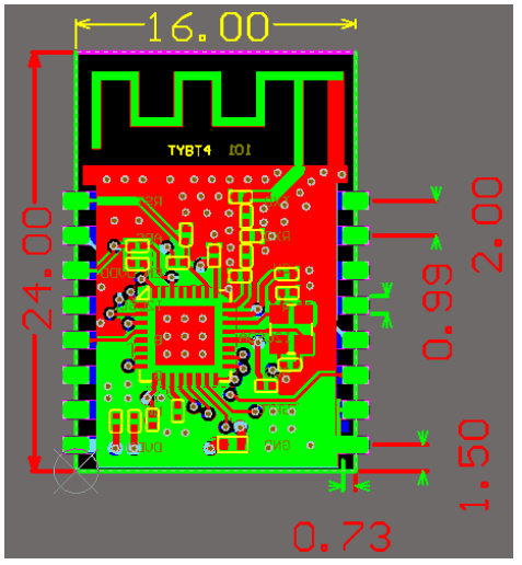
Dimensions and footprint
Dimensions
TYBT4 has double sides of pins, total 16 pins. The distance between each Pin is 2.0mm.
Size of TYBT4: 16mm(W) × 24mm(L).
Figure 2 shows the dimensions of TYBT4.
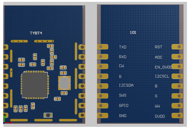
Pin definition
Table 1 shows the general pin attributes of TYBT4.
| Pin No. | Name | Type | Description |
|---|---|---|---|
| 1 | RST | I | Reset pin for the module, Internal pull-up 4.7k resistance |
| 2 | ADC | I | External analog signal input |
| 3 | EN | I | Enable. No need for the internal pull-up. It is connected to DVDD (3.3V) internally |
| 4 | I2CSCL | I/O | I2C, clock interface. Can be used as normal GPIO, while used for the I2C clock signal, Need external pull-up 4.7k resistance |
| 5 | PWM4 | I/O | normal IO pin, can be used as PWM output pin, default for blue LED line |
| 6 | PWM3 | I/O | normal IO pin, can be used as PWM output pin, default for Green LED line |
| 7 | PWM1 | I/O | normal IO pin, can be used as PWM output pin, default for warm white LED line |
| 8 | VCC | P | Supply voltage, range from 1.9 to 3.6V |
| 9 | GND | P | Ground |
| 10 | GPIO | I/O | Reserved GPIO |
| 11 | SWS | I/O | Bluetooth chipset burning pin |
| 12 | I2CSDA | I/O | I2C, data interface. Can be used as normal GPIO, while used for I2C SDA signal, Need external pull-up 4.7k resistance |
| 13 | PWM2 | I/O | Normal IO pin, which can be used as PWM output pin, default for Red LED line |
| 14 | PWM0 | I/O | Normal IO pin, which can be used as PWM output pin, default for cold white line |
| 15 | U_RX | I/O | UART RX, which can be used as a normal IO pin |
| 16 | U_TX | I/O | UART TX, which can be used as a normal IO pin |
P: Power supply pins; I/O: Digital input or output pins.- SW pin is ONLY used for burning firmware, Can NOT be used for other functions.
- While Pin4 and Pin12 are used for I2C functions, external 4.7k pull-up resistances are necessary.
- When the PWM1 pin is outputting the PWM signal, it has the opposite phase compared to the PWM signal from PWM2, PWM3, PWM4, and PWM0 pins. If you need any customization of PWM output, please contact our BD manager.
Electrical characteristics
Absolute maximum ratings
Table 2. Absolute maximum ratings
| Parameter | Description | Min. | Max. | Unit |
|---|---|---|---|---|
| Ts | Storage temperature | -20 | 85 | °C |
| VCC | Supply voltage | -0.3 | 3.9 | V |
| Electrostatic release quantity (Human body model) | TAMB-25°C | - | 2 | KV |
| Electrostatic release quantity (Machine model) | TAMB-25°C | - | 0.5 | KV |
Electrical conditions
Table 3. Electrical conditions
| Parameter | Description | Min. | Typical | Max. | Unit |
|---|---|---|---|---|---|
| Ta | Temperature for Commercial grade | -20 | - | 85 | °C |
| VCC | Supply voltage | 2.5 | 3.3 | 3.6 | V |
| VIL | IO negative level input | -0.3 | - | VCC*0.25 | V |
| VIH | IO positive level input | VCC*0.75 | - | VCC | V |
| VOL | IO negative level output | - | - | VCC*0.1 | V |
| VoH | IO positive level output | VCC*0.8 | - | VCC | V |
Transmitting current consumptions
Table 4. TX current consumption
| Parameter | Mode | Typical | Unit |
|---|---|---|---|
| Itx | Continuously transmitting, 0dBm power output | 13 | mA |
| Irx | Continuously receiving | 13 | mA |
| IDC | Normal working mode | 80 | μA |
Radio specification
Basic radio frequency characteristics
Table 5. Basic radio frequency characteristics
| Parameter | Description |
|---|---|
| Working Frequency | 2.4GHz ISM band |
| Radio standard | Bluetooth 4.0 |
| Data transmitting rate | 1Mbps, 2Mbps |
| Type of Antenna | On-board PCB Antenna |
Transmitting power
Table 6. Transmitting power
| Parameter | Min. | Typical | Max. | Unit |
|---|---|---|---|---|
| RF Average output power consumption | 3.8 | 7 | - | dBm |
| 20dB bandwidth | - | 1000 | - | KHz |
Receiving sensitivity
Table 7. Receiving sensitivity
| Parameter | Rate | Min | Typical | Max. | Unit |
|---|---|---|---|---|---|
| RX sensitivity | 1Mbps | -93 | -92 | -90 | dBm |
| Frequency bias error | - | -300 | - | +300 | KHz |
| Co-channel interference Restrain | - | - | -7 | - | dB |
Antenna information
Antenna type
The TYBT4 module uses a 2.4 GHz onboard PCB antenna.
Reduce antenna interference
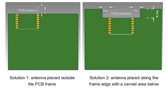
In order to have the best RF performance, it is recommended to keep a minimum 15mm distance between the antenna part and the other metal pieces.
Since PCBA manufacturers use the SMT process to weld the TYBT4 module and other electrical components onto the PCB board, RF performance will depend on the layout location and pattern of the onboard PCB antenna. The following figures are some recommended and dis-recommended demonstrations from our R&D team.
In demonstrations 1 and 2 of Figure 3, the onboard PCB antenna lies outside of the PCB frame. It is recommended to use the layout pattern shown in demonstrations 1 and 2. Either the onboard PCB antenna lays outside of the PCB frame directly or the PCB frame carves out a certain area for the antenna. The overall PCBA performance for these two ways will be the same as testing the module independently.
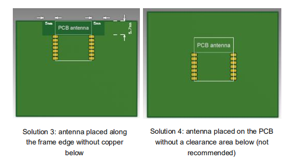
Restricted due to some reason, if the onboard PCB antenna layout has to be inside the PCB frame, it is suggested to refer to demonstration 3. The antenna lays inside the PCB frame, but no copper or wire beneath the antenna. RF performance will have some loss, approximately 1~2 dBm.
It is NOT recommended to use demonstration 4, the antenna lays inside the PCB frame, and there are copper and wire beneath it. RF performance will have significant attenuation.
Figure 3. Layout demonstrations
Packaging information and production guide
Mechanical dimensions
Figure 4. Dimensions of the module
Production guide
The storage for the delivered module should meet the following condition:
- The anti-moisture bag should be kept in an environment with temperature < 30℃ and humidity < 85% RH.
- The expiration date is 6 months since the dry packaging products are sealed.
Cautions:
- All the operators should wear an electrostatic ring throughout the whole process of production.
- While operating, water and dirt should not have any contact with the modules.
Is this page helpful?
YesFeedbackIs this page helpful?
YesFeedback


