Hardware Design Reference
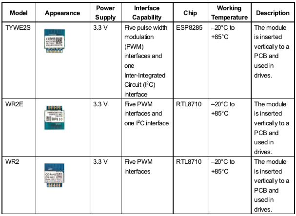
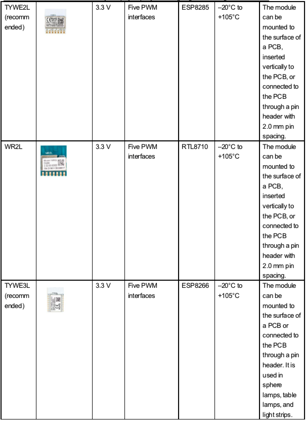
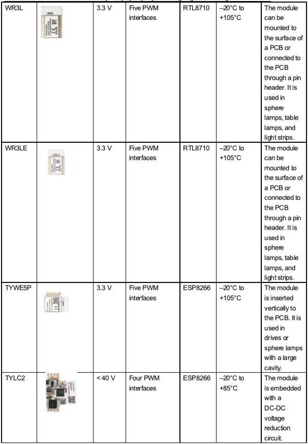
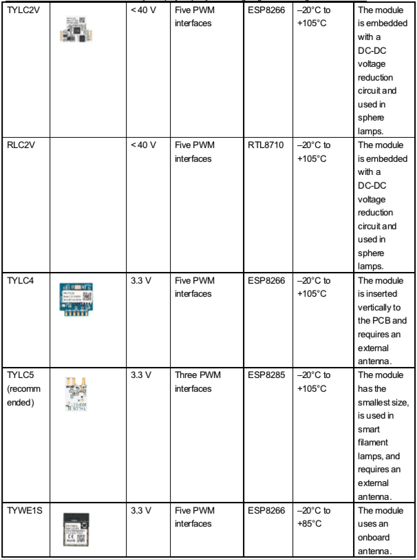
Step 1: Select a Module
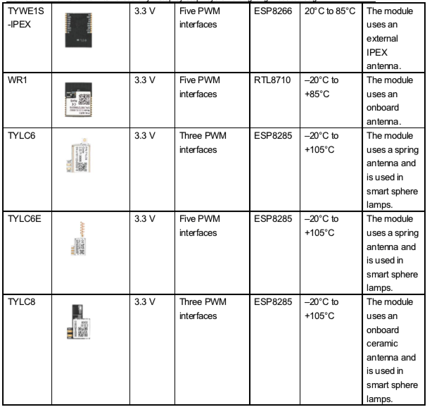
Wi-Fi Modules
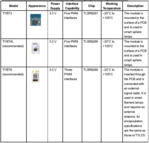
Bluetooth mesh Modules (Tuya)
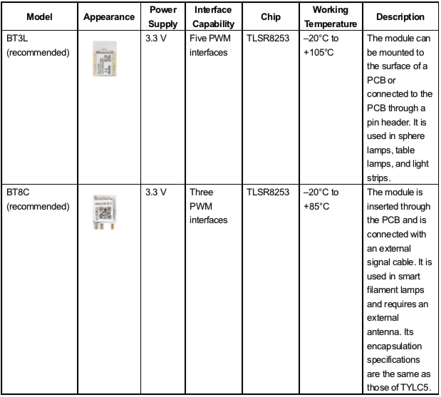
Bluetooth mesh Modules (SIG)
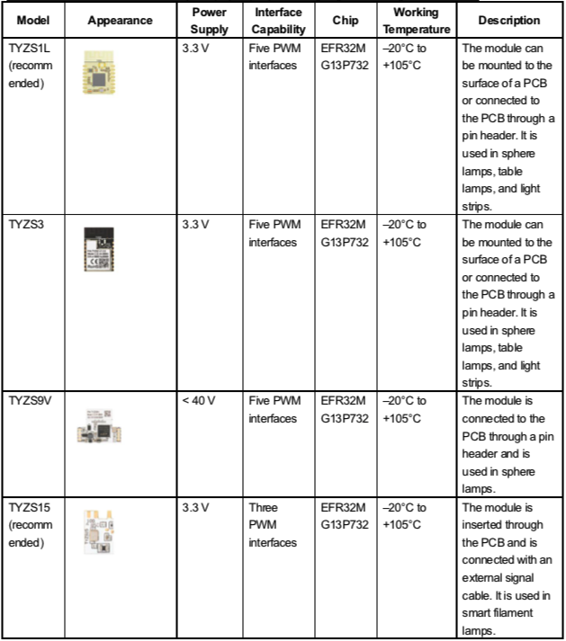
Zigbee Modules
Step 2: Select a Module Power Supply Mode
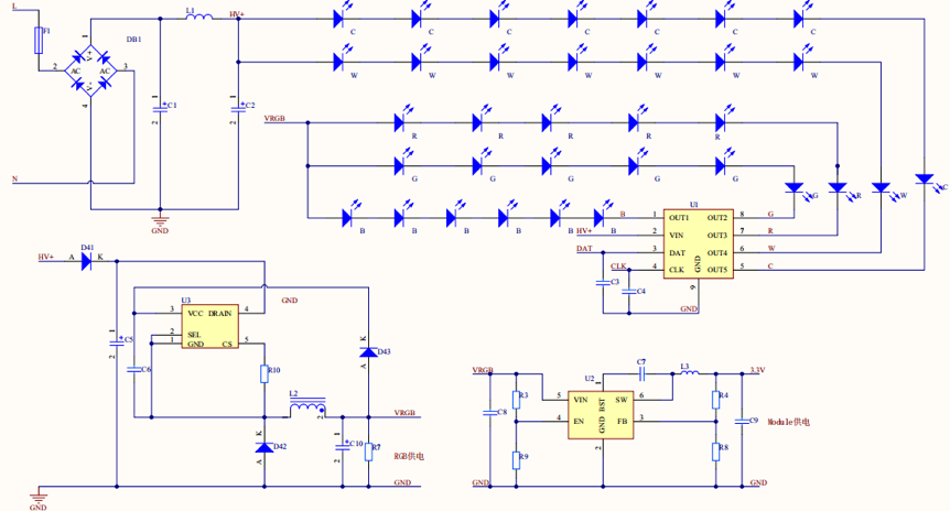
AC-DC Constant-Voltage Power Supply
- A module’s normal working voltage range is 3.0 V to 3.6 V.
- If the output voltage is higher than 3.3 V, consider the output voltage ripple and output power in addition to the power to the module to prevent insufficient power supply to the module due to undervoltage output. The power supply system must ensure a stable power supply voltage under the maximum output power.
- If the output voltage is the module’s power supply voltage or 3.3 V, set the output voltage central value to 3.3 V to have a ripple voltage of less than 100 mV and an average Wi-Fi module current of about 80 mA. The AC-DC power supply system must generate 200 mA current on average. The peak value of the dynamic output current of the power supply system must reach 450 mA, and the output voltage is not lower than 2.8V. The 3.3 V Wi-Fi module’s power supply pin is connected to a 0.1 μF ceramic capacitor to reduce interference. To power a 3.3 V Bluetooth or Zigbee module, the AC-DC power supply system must have a ripple voltage of less than 100 mV and can generate 50 mA current on average. When the dynamic output current is 100 mA, the output voltage is not lower than 2.8V.
- In low standby power application scenarios, select the low standby power AC-DC drive chip and a module with low standby current.
- Use a diode and capacitor to isolate the AC-DC power supply circuit from the main power (highlighted with the red rectangle in the following figure) to prevent the working module from affecting the main power, especially the linear constant-current drive power source, so that light jitter will not occur.
DC-DC Constant-Voltage Power Supply
- When a module embedded with a DC-DC voltage reduction circuit is powered by DC voltage, the DC voltage cannot exceed 40 V.
- When the DC voltage exceeds 3.3 V, use a voltage reduction chip to reduce the voltage to 3.3 V. A switch-type voltage reduction control chip is recommended, as shown in the following figure. To power a 3.3 V Wi-Fi module, the DC-DC power supply system must have a ripple voltage of less than 100 mV and can generate a 200 mA current. When the dynamic output current is 450 mA, the the output voltage is not lower than 2.8V The 3.3 V Wi-Fi module’s power supply pin is connected to a 0.1 μF ceramic capacitor to reduce interference. To power a 3.3 V Bluetooth or Zigbee module, the DC-DC power supply system must have a ripple voltage of less than 100 mV and can generate 50 mA current on average. When the dynamic output current is 100 mA, the output voltage is not lower than 2.8V.
- Low dropout (LDO) regulators are not recommended for powering Wi-Fi modules. If an LDO regulator is used, use a chip with a 500 mA or higher power supply current and ensure good heat dissipation. When the input voltage is higher than 5 V, a switch-type power chip is recommended.
Step 3: Install the Module and Antenna
Similar to light, wireless signals may be blocked by metal in the transmission path. If an antenna is mounted on a metal surface, the module cannot work properly.
To use a module in a sphere lamp, ensure that the module’s antenna is out of the opening groove of the alumina substrate and that the onboard antenna is higher than the alumina substrate. When the light source is not affected and there are no shadows, position the antenna out of the lamp cup’s shielding environment as much as possible.
When using a module in a lamp with a metal cover, for example, a downlight or spotlight lamp or lamp used outdoors, consider the antenna RF design and use an external antenna if needed.
To use a module in a drive, keep the module away from components such as the transformer and inductor.
Step 4: Select an LED Light Driving Method
AC-DC Constant-Current Driver for Monochromatic Lamps (W)
- Switch-type AC-DC constant-current driver, as shown in the following figure
Advantages: high efficiency, high power factor (PF), good constant-current characteristics, high linearity, and adjustable, wide output voltage range
Disadvantages: strong electromagnetic interference (EMI), high cost, noise during PWM light adjustment, and complex PCB layout
The module generates PWM signals.
- Linear AC-DC constant-current driver
Advantages: low cost, no EMI issue, simple PCB layout, and no noise during PWM light adjustment
Disadvantages: low efficiency, narrow voltage range, poor constant-current characteristics, poor linearity, fixed output voltage, and low PF
The module generates PWM signals.
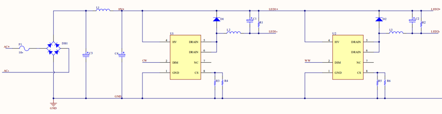
AC-DC Constant-Current Driver for Bi-Color Lamps (CW)
The solution has the CW and CCT control modes. The CW mode uses 2-channel PWM signals for simultaneous control of the brightness and color temperature. The 2-channel PWM signals are CW and WW signals, which respectively control the white light with a high color temperature and warm light with a low color temperature. During 1-channel light adjustment, CW signals are used. The CCT mode uses 2-channel PWM signals for separate control of the brightness and color temperature. The Bright signals control the brightness, and the CCT signals control the color temperature. For details, see the pin configuration.
- Switch-type AC/DC constant-current driver in CW mode
Advantages: high efficiency, good constant-current characteristics, high linearity, and good light adjustment
Disadvantages: strong EMI, circuit noise, large color temperature offset when the duty cycle is small, complex circuit layout, and high cost
The module generates 2-channel PWM signals: CW and WW.
- Linear AC-DC constant-current driver in CW mode
Advantages: low cost, no EMI issue, simple PCB layout, and no noise during PWM light adjustment
Disadvantages: low efficiency, narrow voltage range, poor constant-current characteristics, poor linearity, fixed output voltage, and large color temperature offset when the duty cycle is small
The module generates 2-channel PWM signals: CW and WW.
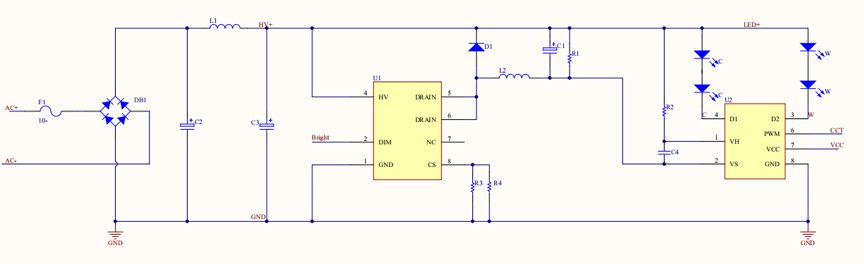
- AC-DC constant-current driver in CCT mode
Advantages: high efficiency, good constant-current characteristics, high linearity, basically no color temperature offset, good light adjustment, simulated brightness control, low cost, simple circuit layout, and no noise
Disadvantages: strong EMI and higher cost than the linear AC-DC constant-current driver in CW mode
The module generates 2-channel PWM signals: Bright and CCT.
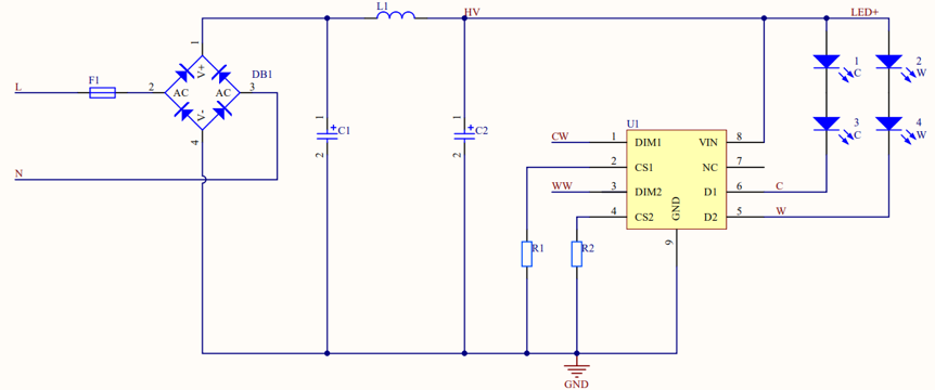
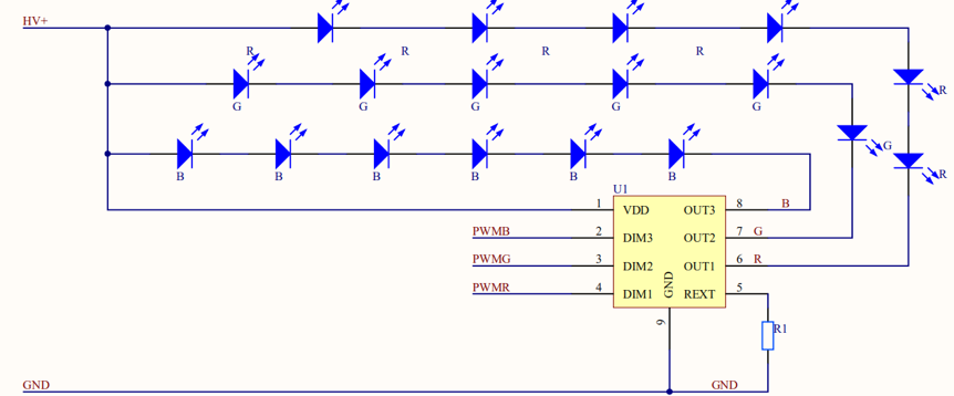
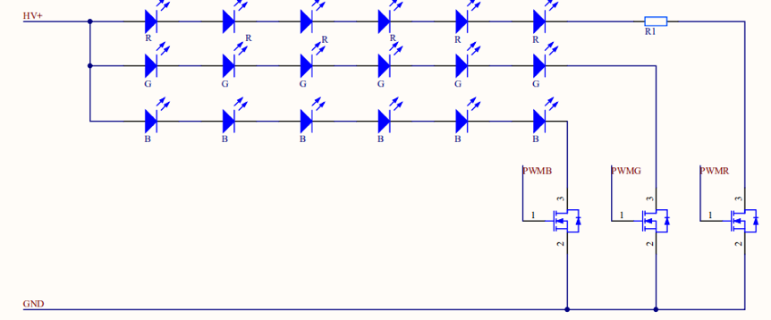
Constant-Current Driver for RGB Lamps
- DC-DC PWM-controlled linear constant-current driver
The module generates 3-channel PWM signals: PWMR, PWMG, and PWMB. The linear constant-current driver ensures constant RGB current output.
- DC-DC I2C-controlled linear constant-current driver
The I2C DAT and CLK signals can control RGB or RGBCW lamps, requiring only several control pins. The module generates I2C DAT and CLK signals to the driver chip to ensure a constant RGB current. To use the I2C solution, pay attention to the PCB layout. I2C signals are vulnerable to interference from switch signals (AC-DC drive circuit). If the interference is serious, add a 10 pF to 50 pF filter capacitor to the DAT and CLK signal circuits during PCB layout design to reduce interference.
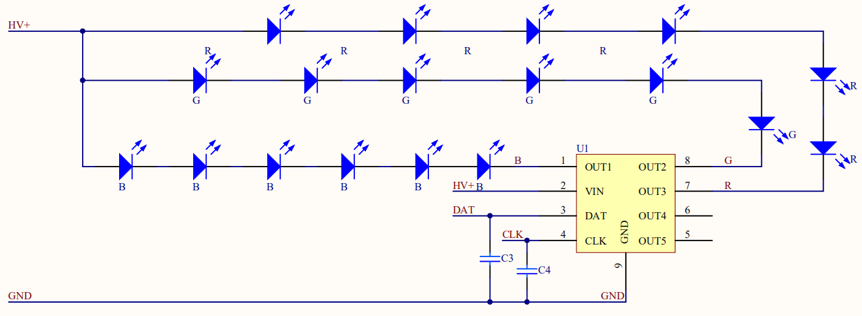
Note: Pull-up resistors need to be added to the physical circuits of the peripheral I2C DAT and CLK signals. Typically, the resistance value is 4.7 kiloohms, which can be adjusted based on the actual scenario.
- DC-DC PWM-controlled BJT/MOSFET switch driver
Use the BJT or MOSFET switch to control RGB through PWM signals. The RGB current is variable and discrete. Add a resistor for the red light control channel to limit the current because the red light diode has a low voltage. In this case, under the same input conditions as the constant-current solution, the loss is increased. Note: The bead voltage cannot be greatly different from the input voltage.
AC-DC I2C-controlled Linear Constant-Current Driver for RGBCW Lamps
Advantages: a simple solution, simple peripheral parameters, low cost, and requires only the DAT and CLK signals for control
Disadvantages: driven by linear constant current, and DAT and CLK signals are vulnerable to interference
Note: The RGB light needs to be powered separately. An AC-DC + DC-DC power supply solution is recommended.
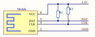
Step 5: Define Module Pins
In network configuration mode, the CW pin generates a high or low level to indicate the network configuration status.
The CW pin is used for 1-channel light control. For cold and warm light control in CW mode, the CW and WW pins control the cold and warm light, respectively. In CCT control mode, the Bright and CCT pins respectively control the brightness and color temperature.
The following tables define the module pins.
WIFI:
Espressif Systems:
TYWE3S TYWE3L TYWE5P
|I/O Interface| W |CW | CCT | RGB(PWM) | RGB (I2C) |
|:-------|:-------|:-------|:---------|:-----|:-------|:-------|
|IO5 |W| CW | Bright| | |
|IO13 || WW | CCT| | |
|IO4 || | | R | SCL|
|IO12 || | |G | |
|IO14 || | | B|SDA |
|IO16 || | | | Low-power |
TYWE3SE
|I/O Interface| W |CW | CCT | RGB(PWM) | RGB (I2C) |
|:-------|:-------|:-------|:---------|:-----|:-------|:-------|
|IO22 |W| CW | Bright| | |
|IO13 || WW | CCT| | |
|IO5 || | | R | SCL|
|IO25 || | |G | |
|IO14 || | | B|SDA |
|IO33 || | | | Low-power |
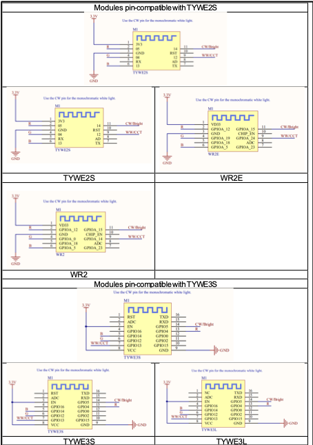
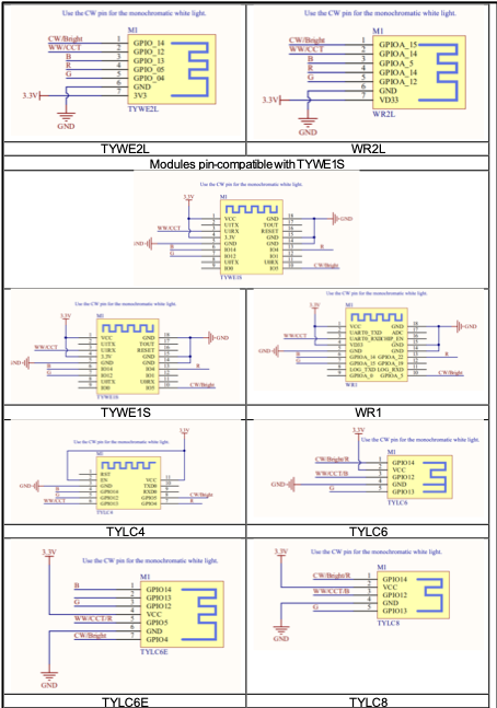
TYWE1S TYLC4
|I/O Interface| W |CW | CCT | RGB(PWM) | RGB (I2C) |
|:-------|:-------|:-------|:---------|:-----|:-------|:-------|
|IO5 |W| CW | Bright| | |
|IO13 || WW | CCT| | |
|IO4 || | | R | SCL|
|IO12 || | |G | Low-power |
|IO14 || | | B|SDA |
TYWE2S TYWE2L
|I/O Interface| W |CW | CCT | RGB(PWM) | RGB (I2C) |
|:-------|:-------|:-------|:---------|:-----|:-------|:-------|
|IO14 |W| CW | Bright| | |
|IO12 || WW | CCT| | |
|IO5 || | | R | SCL|
|IO4 || | |G | Low-power |
|IO13 || | | B|SDA |
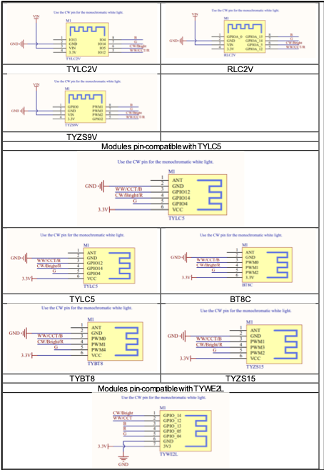
TYLC5
|I/O Interface| W |CW | CCT | RGB(PWM) | RGB (I2C) |
|:-------|:-------|:-------|:---------|:-----|:-------|:-------|
|IO14 |W| CW |Bright | R | SCL|
|IO12 || WW |CCT |B | SDA |
|IO4 || | | G|Low-power |
TYLC6 TYLC8
|I/O Interface| W |CW | CCT | RGB(PWM) | RGB (I2C) |
|:-------|:-------|:-------|:---------|:-----|:-------|:-------|
|IO14 |W| CW |Bright | R | SCL|
|IO12 || WW |CCT |B | SDA |
|IO13 || | | G|Low-power |
TYLC6E
|I/O Interface| W |CW | CCT | RGB(PWM) | RGB (I2C) |
|:-------|:-------|:-------|:---------|:-----|:-------|:-------|
|IO4 |W| CW |Bright | | |
|IO5|| WW |CCT |R | |
|IO12 || | | G|SDA |
|IO14 || | | B|SCL |
|IO13 || | | |Low-power |
TYLC2V
|I/O Interface| W |CW | CCT | RGB(PWM) | RGB (I2C) |
|:-------|:-------|:-------|:---------|:-----|:-------|:-------|
|IO5 |W| CW |Bright | | |
|IO12|| WW |CCT |R | |
|IO14 || | | G|SDA |
|IO4 || | | B|SCL |
|IO13 || | | |Low-power |
Realtek module pins:
WR1 (Pin-compatible with TYWE1S)
|I/O Interface| W |CW | CCT | RGB(PWM) | RGB (I2C) |
|:-------|:-------|:-------|:---------|:-----|:-------|:-------|
|GPIOA_5 |W| CW |Bright | | |
|GPIOA_18|| WW |CCT | | |
|GPIOA_22 || | | R|SCL |
|GPIOA_15 || | | G|Low-power |
|GPIOA_14 || | | B |SDA |
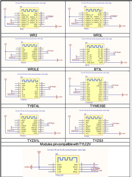
WR3 and WR3L (Pin-compatible with TYWE3S and TYWE3L)
|I/O Interface| W |CW | CCT | RGB(PWM) | RGB (I2C) |
|:-------|:-------|:-------|:---------|:-----|:-------|:-------|
|GPIOA_12 |W| CW |Bright | | |
|GPIOA_0|| WW |CCT | | |
|GPIOA_5 || | | R|SCL |
|GPIOA_15 || | | G| |
|GPIOA_14 || | | B |SDA |
|GPIOA_19 || | | | Low-power|
WR3E and WR3LE (Pin-compatible with TYWE3S and TYWE3L)
|I/O Interface| W |CW | CCT | RGB(PWM) | RGB (I2C) |
|:-------|:-------|:-------|:---------|:-----|:-------|:-------|
|GPIOA_12 |W| CW |Bright | | |
|GPIOA_22|| WW |CCT | | |
|GPIOA_5 || | | R|SCL |
|GPIOA_15 || | | G| |
|GPIOA_14 || | | B |SDA |
|GPIOA_29 || | | | Low-power|
WR5P (Pin-compatible with TYWE5P)
|I/O Interface| W |CW | CCT | RGB(PWM) | RGB (I2C) |
|:-------|:-------|:-------|:---------|:-----|:-------|:-------|
|GPIOA_12 |W| CW |Bright | | |
|GPIOA_5|| WW |CCT | | |
|GPIOA_14 || | | R|SCL |
|GPIOA_15 || | | G| |
|GPIOA_0 || | | B |SDA |
|GPIOA_22 || | | | Low-power|
RLC2V and RLC7V (Pin-compatible with TYLC2V)
|I/O Interface| W |CW | CCT | RGB(PWM) | RGB (I2C) |
|:-------|:-------|:-------|:---------|:-----|:-------|:-------|
|GPIOA_5 |W| CW |Bright | | |
|GPIOA_12|| WW |CCT |R | |
|GPIOA_14 || | | G|SDA |
|GPIOA_15 || | | B| SCL|
|GPIOA_0 || | | |Low-power |
RLC4 (Pin-compatible with TYLC4)
|I/O Interface| W |CW | CCT | RGB(PWM) | RGB (I2C) |
|:-------|:-------|:-------|:---------|:-----|:-------|:-------|
|GPIOA_5 |W| CW |Bright | | |
|GPIOA_12|| WW |CCT | | |
|GPIOA_19 || | | R|SCL |
|GPIOA_15 || | | G| Low-power|
|GPIOA_14 || | | B |SDA |
WR2L (Pin-compatible with TYWE2L)
|I/O Interface| W |CW | CCT | RGB(PWM) | RGB (I2C) |
|:-------|:-------|:-------|:---------|:-----|:-------|:-------|
|GPIOA_15 |W| CW |Bright | | |
|GPIOA_14|| WW |CCT | | |
|GPIOA_19 || | | R|SCL |
|GPIOA_12 || | | G| Low-power|
|GPIOA_5 || | | B |SDA |
WR2E (Pin-compatible with TYWE2S)
|I/O Interface| W |CW | CCT | RGB(PWM) | RGB (I2C) |
|:-------|:-------|:-------|:---------|:-----|:-------|:-------|
|GPIOA_15 |W| CW |Bright | | |
|GPIOA_24|| WW |CCT | | |
|GPIOA_12 || | | R|SCL |
|GPIOA_19 || | | G| Low-power|
|GPIOA_5 || | | B |SDA |
WR2 (Pin-compatible with TYWE2S)
|I/O Interface| W |CW | CCT | RGB(PWM) | RGB (I2C) |
|:-------|:-------|:-------|:---------|:-----|:-------|:-------|
|GPIOA_15 |W| CW |Bright | | |
|GPIOA_14|| WW |CCT | | |
|GPIOA_12 || | | R|SCL |
|GPIOA_0 || | | G| Low-power|
|GPIOA_5 || | | B |SDA |
Tuya Bluetooth mesh module pins:
TYBY3
|I/O Interface| W |CW | CCT | RGB(PWM) | RGB (I2C) |
|:-------|:-------|:-------|:---------|:-----|:-------|:-------|
|GPIOA_15 |W| CW |Bright | | |
|GPIOA_14|| WW |CCT | | |
|GPIOA_12 || | | R|SCL |
|GPIOA_0 || | | G| Low-power|
|GPIOA_5 || | | B |SDA |
TYBT4L (Pin-compatible with TYWE3S)
|I/O Interface| W |CW | CCT | RGB(PWM) | RGB (I2C) |
|:-------|:-------|:-------|:---------|:-----|:-------|:-------|
|GPIOA_15 |W| CW |Bright | | |
|GPIOA_14|| WW |CCT | | |
|GPIOA_12 || | | R|SCL |
|GPIOA_0 || | | G| |
|GPIOA_5 || | | B |SDA |
|GPIOA_5 || | | |Low-power|
TYBT8 (Pin-compatible with TYLC5)
|I/O Interface| W |CW | CCT | RGB(PWM) | RGB (I2C) |
|:-------|:-------|:-------|:---------|:-----|:-------|:-------|
|PWM1 |W| CW |Bright | R | SCL |
|PWM0|| WW |CCT |B | SDA|
|PWM4 || | | G|Low-power |
SIG Bluetooth mesh module pins:
BT3L (Pin-compatible with TYWE3S)
|I/O Interface| W |CW | CCT | RGB(PWM) | RGB (I2C) |
|:-------|:-------|:-------|:---------|:-----|:-------|:-------|
|TL_B5 |W| CW |Bright | | |
|TL_C2|| WW |CCT | | |
|TL_B4 || | | R|SCL |
|TL_C3 || | | G| |
|TL_D2 || | | B |SDA |
|TL-D7 || | | |Low-power|
BT8C (Pin-compatible with TYLC5 and TYBT8)
|I/O Interface| W |CW | CCT | RGB(PWM) | RGB (I2C) |
|:-------|:-------|:-------|:---------|:-----|:-------|:-------|
|PWM1 |W| CW |Bright | R | SCL |
|PWM0|| WW |CCT |B | SDA|
|PWM4 || | | G|Low-power |
Zigbee module pins
TYZS3 and TYZS1L (Pin-compatible with TYWE3S)
|I/O Interface| W |CW | CCT | RGB(PWM) | RGB (I2C) |
|:-------|:-------|:-------|:---------|:-----|:-------|:-------|
|GPIO3|W| CW |Bright | | |
|PWM1|| WW |CCT | | |
|PWM2|| | | R|SCL |
|PWM3 || | | G| |
|SWO || | | B |SDA |
|GPIO0|| | | |Low-power|
TYZS15 (Pin-compatible with TYLC5, TYBT8, and BT8C)
|I/O Interface| W |CW | CCT | RGB(PWM) | RGB (I2C) |
|:-------|:-------|:-------|:---------|:-----|:-------|:-------|
|PWM3 |W| CW |Bright | R | SCL |
|PWM1|| WW |CCT |B | SDA|
|PWM2 || | | G|Low-power |
TYZS9V (Pin-compatible with TYLC2V)
|I/O Interface| W |CW | CCT | RGB(PWM) | RGB (I2C) |
|:-------|:-------|:-------|:---------|:-----|:-------|:-------|
|PWM2|W| CW |Bright | | |
|GPIO2|| WW |CCT |R | |
|PWM3|| | | G|SDA|
|PWM1 || | | B |SCL |
|GPIO0|| | | |Low-power|
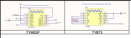
The following figures show pins on some modules:
When the Espressif Systems 8266 chip is being powered on, some I/O interfaces are unstable and have weak output with a high pulse for 180 ms during initialization. As a result, the high level-driven light blinks. To prevent this scenario, connect pull-down resistors whose resistance is less than or equal to 3.3 kiloohms to these I/O interfaces. A lower resistance may be required according to the peripheral circuit. For details, see the following initial pin status table.
Initial pin status:
| Pin | Initial Status | Recommended Configuration |
|---|---|---|
| IO2 | Pulled up | Add an external pull-down resistor. |
| IO4 | High resistance | Add an external pull-down resistor. |
| IO5 | High resistance | Add an external pull-down resistor. |
| IO12 | Pulled up | Add an external pull-down resistor. |
| IO13 | Pulled up | Add an external pull-down resistor. |
| IO14 | Pulled up | Add an external pull-down resistor. |
| IO15 | Low-level | |
| IO16 | High-level |
Is this page helpful?
YesFeedbackIs this page helpful?
YesFeedback


