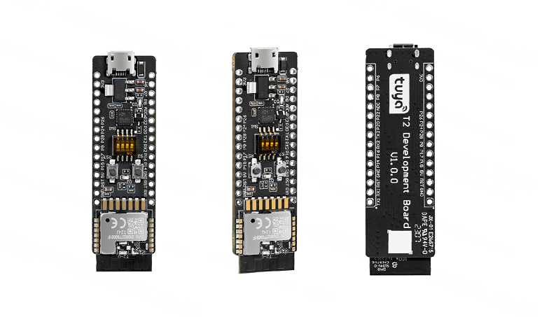
T2-U Development Board
T2-U development board is designed for prototyping smart devices easily and quickly. You can use it with other purpose-built modules or development boards to evaluate your project.
Scenarios
T2-U development board applies to a wide range of scenarios.
- Develop with the board to build your IoT projects easily and fast.
- You can use this board for different development purposes.
- Embedded program development and debugging
- App development and debugging
- Creating connected devices that can be controlled with a mobile phone
- Getting started with IoT development and learning how the Wi-Fi-enabled control system works
Components
T2-U development board consists of Tuya’s highly-integrated Wi-Fi and Bluetooth module T2-U and peripherals including buttons, LED indicator, GPIOs, power, and USB-to-serial chip.
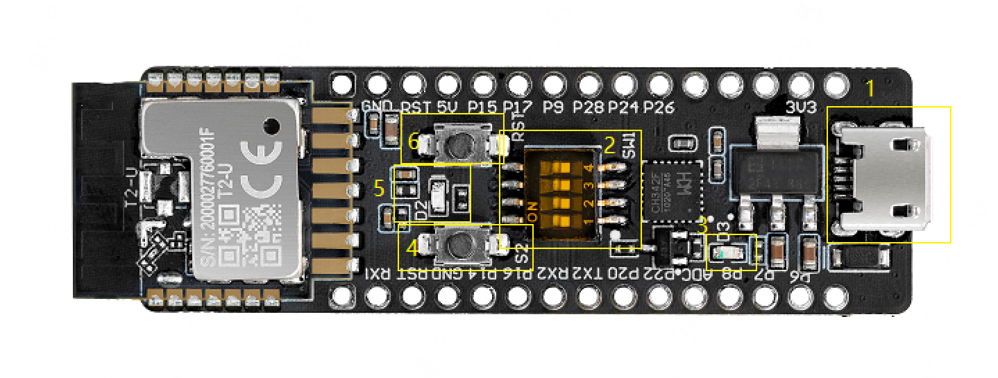
I/O port functions
-
1: Micro-USB (CN1): Inputs 5V DC voltage and provides two extended serial ports.
-
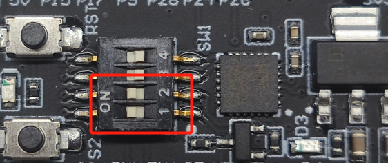
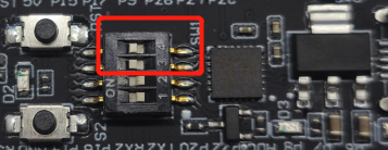
2: DIP switch (S1): Flip the toggle to the ON position to complete the circuit. The switch is used to open and close the circuit between the USB-to-serial chip and the chip’s serial port.
-
3: LED indicator (D3): When the 3.3V power is on, the LED is on.
-
4: Button (S2): When the button is pressed, P7 outputs low. When the button is released, it outputs high.
-
5: LED indicator (D2): When P26 outputs low, the LED is on.
-
6: Button (RST): When the button is pressed, the module is reset.
Pin description
No. Symbol Description 1 NC Leave it floating. 2 3.3V 3.3V power pin. 3 NC Leave it floating. 4 NC Leave it floating. 5 NC Leave it floating. 6 P26 Support hardware PWM5, corresponding to Pin 15 on the IC. 7 P24 Support hardware PWM4, corresponding to Pin 16 on the IC. 8 P28 A normal GPIO pin on T2-U, corresponding to Pin 10 on the IC. 9 P9 A normal GPIO pin on T2-U, corresponding to Pin 25 on the IC. 10 P17 A normal GPIO pin on T2-U, corresponding to Pin 14 on the IC. It can be reused as SPI_MISO.11 P15 A normal GPIO pin on T2-U, corresponding to Pin 13 on the IC. It can be reused as SPI_CS. It is not recommended to use this pin for non-SPI applications.12 5V 5V power pin. 13 RST Clock enable (CEN) pin on T2-U. It can output the chip enable and high enable signals. 14 GND Ground pin. 15 NC Leave it floating. 16 TX1 UART_TX1on T2-U to send user data, corresponding to Pin 27 on the IC.17 RX1 UART_RX1on T2-U to receive user data, corresponding to Pin 26 on the IC.18 RST Clock enable (CEN) pin on T2-U. It can output the high enable signal. 19 GND Ground pin. 20 P14 A normal GPIO pin on T2-U, corresponding to Pin 11 on the IC. It can be reused as SPI_SCK.21 P16 A normal GPIO pin on T2-U, corresponding to Pin 12 on the IC. It can be reused as SPI_MOSI.22 RX2 UART_RX2on T2-U to receive user data, labeledP1, corresponding to Pin 28 on the IC.23 TX2 UART_TX2on T2-U to print logs, labeledP0, corresponding to Pin 29 on the IC.24 P20 A normal GPIO pin on T2-U, corresponding to Pin 20 on the IC. 25 P22 A normal GPIO pin on T2-U, corresponding to Pin 18 on the IC. 26 ADC ADCon T2-U, labeledP23, corresponding to Pin 17 on the IC.27 P8 Support hardware PWM2, corresponding to Pin 24 on the IC. 28 P7 Support hardware PWM1, corresponding to Pin 23 on the IC. 29 P6 Support hardware PWM0, corresponding to Pin 22 on the IC. 30 NC Leave it floating.
Load-carrying capacity
-
When micro-USB (CN1) inputs 5V DC voltage, the board can supply power to external components.
Power pin Rated voltage/current 5V Depends on the input current of the adapter connected to the DC-005 terminal. 3.3V 3.3V/0.6A -
Characteristics of output voltage
Output current 0A 0.15A 0.3A 0.45A 0.6A 0.75A Output voltage 3.34V 3.36V 3.37V 3.37V 3.38V 3.38V We tested the voltage under the condition that there is no output voltage on the micro-USB (CN1) terminal.
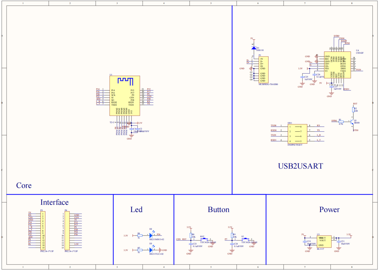
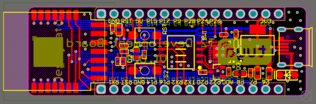
Schematic diagram and PCB
-
The schematic diagram of the board:
-
The PCB board:
USB to serial
The board has a built-in USB-to-serial chip. The single-channel USB port can provide two extended serial ports. You can flip the DIP switch (SW1) to enable the 2-channel serial port on the T2-U to connect to the USB-to-serial chip. The following table lists the pin definition of the DIP switch.
| DIP switch No. | 1 | 2 | 3 | 4 |
|---|---|---|---|---|
| Pin on the chip | UART1_RX | UART1_TX | UART2_RX | UART2_TX |
| USB-to-serial chip | USB-TX0 | USB-RX0 | USB-TX1 | USB-RX1 |
-
Flip the toggle to the ON position to complete the circuit. The switch is used to open and close the circuit between the USB-to-serial chip and the chip’s serial port.
-
When you use the UART pin on the chip for communication with an MCU or GPIO, flip the toggle of the corresponding channel to the OFF position (the side with numbers) to open the circuit between the UART on T2-U and the USB-to-serial chip.
-
The COM port number varies depending on the computers.
Connection for DOWNLOAD mode
The following figure shows the setup for flashing firmware using Tuya’s flashing and authorization software. Flip the toggles of channels 1 and 2 on the DIP switch (SW1) to the ON position to complete the circuit between the UART1 on T2-U and the host.
Typically, the module on the development board comes pre-flashed with firmware.
Connection for viewing logs on the host
Flip the toggles of channels 3 and 4 on the DIP switch (SW1) to the ON position to complete the circuit between the UART2 on T2-U and the host.
USB-to-serial chip driver
Download the USB-to-serial chip driver for your operating system.
Things to note
- The board has a built-in power supply port and circuit, so the additional power board is not necessary.
- This board only supports a USB port that supplies 5V output.
Is this page helpful?
YesFeedbackIs this page helpful?
YesFeedback


