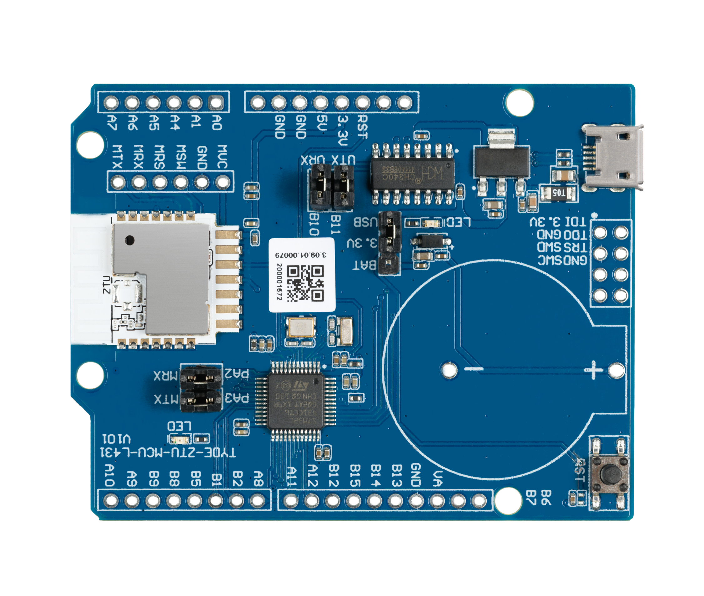
Zigbee ST(L4) Board (ZTU)
This ultra-low-power consumption development board comes with a ZTU Zigbee module and an STM32L431CC microcontroller (MCU) from STMicroelectronics. It can work with circuit modules or boards to help you prototype ideas and evaluate solutions.
Applications
- This development board applies to most custom solutions developed with the MCU SDK. You can use it to build Zigbee projects where the network modules communicate with the MCU through the serial protocol.
- Develop with the board to build your IoT projects easily and fast.
- You can use this board for different development purposes.
- Embedded program development and debugging
- App development and debugging
- Creating connected devices that can be controlled with a mobile phone
- Getting started with IoT development and learning how the Zigbee-based control system works
Components
The development board is integrated with Tuya’s proprietary high-performance ZTU Zigbee module and STM32L431CC MCU from STMicroelectronics. It has onboard MCU reset buttons, LED, power port, and a USB-to-serial chip.
- For more information, see the ZTU Module Datasheet.
- For more information, see Zigbee General Solution.
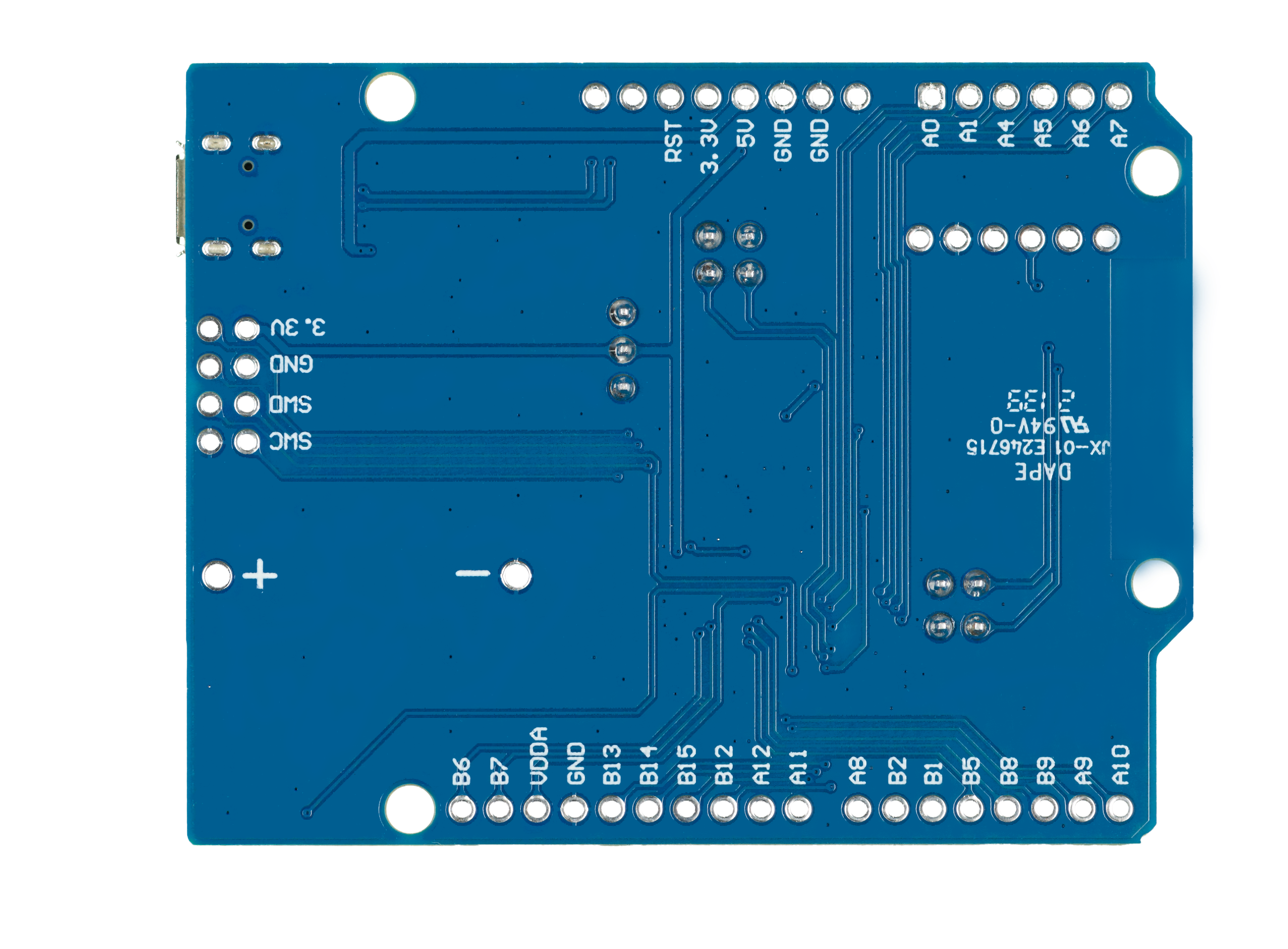
I/O port and pin description
-
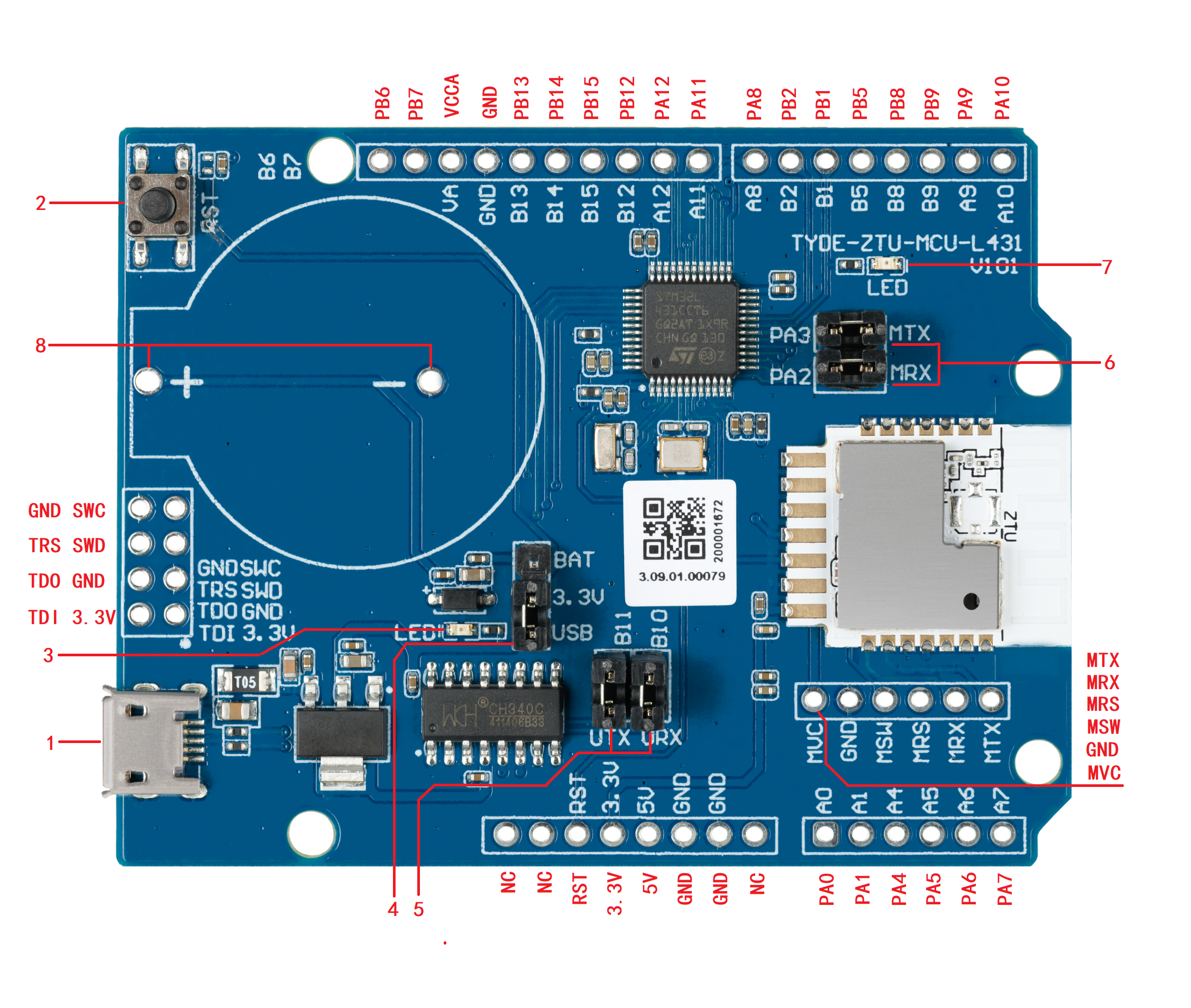
1: Micro-USB: Input 5V DC voltage and provide one extended serial port.
-
2: Button (RST): Reset the STM32L431CC MCU. Press the button to output low level signals.
-
3: LED indicator: Indicate the power state when the board is powered via the micro-USB connection.
-
4: Power selection jumper: Use a jumper cap to switch the power supply between the USB connection and external power supply.
-
5: USB to UART jumper: Use a jumper cap on
PB11andPB10to connect to the USB-to-serial chip. -
6: UART selection jumper: Use a jumper cap on
PA2andPA3to connect the MCU to the ZTU module. -
7: LED indicator: When PB1 outputs high, the LED is on.
-
8: External battery pin header: Connect a button cell to the positive (
+) and negative (-) terminals for verifying low power mode.Pin description
No. Symbol Description Alternate functions 1 NC Leave it floating. - 2 NC Leave it floating. - 3 RST Reset the STM32L431CC MCU. Active low. - 4 3.3V 3.3V power pin. - 5 5V 5V power pin. - 6 GND Ground pin. - 7 GND Ground pin. - 8 NC Leave it floating. - 9 PA0 I/O TIM2_CH1, USART2_CTS, COMP1_OUT, SAI1_EXTCLK, TIM2_ETR, EVENTOUT,OPAMP1_VINP, COMP1_INM, ADC1_IN5, RTC_TAMP2, and WKUP1 10 PA1 I/O TIM2_CH2, I2C1_SMBA, SPI1_SCK, USART2_RTS_DE, TIM15_CH1N, EVENTOUT,OPAMP1_VINM, COMP1_INP, and ADC1_IN6 11 PA4 I/O SPI1_NSS, SPI3_NSS, USART2_CK, SAI1_FS_B, LPTIM2_OUT, EVENTOUT ,COMP1_INM, COMP2_INM, ADC1_IN9, and DAC1_OUT1 12 PA5 I/O TIM2_CH1, TIM2_ETR, SPI1_SCK, LPTIM2_ETR, EVENTOUT, COMP1_INM, COMP2_INM, ADC1_IN10, and DAC1_OUT2 13 PA6 I/O TIM1_BKIN, SPI1_MISO, COMP1_OUT, USART3_CTS, LPUART1_CTS, QUADSPI_BK1_IO3, TIM1_BKIN_COMP2, TIM16_CH1, EVENTOUT, and ADC1_IN11 14 PA7 I/O TIM1_CH1N, I2C3_SCL, SPI1_MOSI, QUADSPI_BK1_IO2, COMP2_OUT, EVENTOUT, and ADC1_IN12 15 PA10 I/O TIM1_CH3, I2C1_SDA, USART1_RX, SAI1_SD_A, and EVENTOUT 16 PA9 I/O TIM1_CH2, I2C1_SCL, USART1_TX, SAI1_FS_A, TIM15_BKIN, and EVENTOUT 17 PB9 I/O IR_OUT, I2C1_SDA, SPI2_NSS, CAN1_TX, SDMMC1_D5, SAI1_FS_A, and EVENTOUT 18 PB8 I/O IR_OUT, I2C1_SDA, SPI2_NSS, CAN1_TX, SDMMC1_D5, SAI1_FS_A, EVENTOUT 19 PB5 I/O LPTIM1_IN1, I2C1_SMBA, SPI1_MOSI, SPI3_MOSI, USART1_CK, TSC_G2_IO2, COMP2_OUT, SAI1_SD_B, TIM16_BKIN, and EVENTOUT 20 PB1 I/O TIM1_CH3N, USART3_RTS_DE, LPUART1_RTS_DE, QUADSPI_BK1_IO0, LPTIM2_IN1, EVENTOUT, COMP1_INM, and ADC1_IN16 21 PB2 I/O RTC_OUT, LPTIM1_OUT, I2C3_SMBA, EVENTOUT, and COMP1_INP 22 PA8 I/O MCO, TIM1_CH1, USART1_CK, SWPMI1_IO, SAI1_SCK_A, LPTIM2_OUT, and EVENTOUT 23 PA11 I/O TIM1_CH4, TIM1_BKIN2, SPI1_MISO, COMP1_OUT, USART1_CTS, CAN1_RX, TIM1_BKIN2_COMP1, and EVENTOUT 24 PA12 I/O TIM1_ETR, SPI1_MOSI, USART1_RTS_DE, CAN1_TX, and EVENTOUT 25 PB12 I/O TIM1_BKIN, TIM1_BKIN_COMP2, I2C2_SMBA, SPI2_NSS, USART3_CK, LPUART1_RTS_DE, TSC_G1_IO1, SWPMI1_IO, SAI1_FS_A, TIM15_BKIN, and EVENTOUT 26 PB15 I/O RTC_REFIN, TIM1_CH3N, SPI2_MOSI, TSC_G1_IO4, SWPMI1_SUSPEND, SAI1_SD_A, TIM15_CH2, and EVENTOUT 27 PB14 I/O TIM1_CH2N, I2C2_SDA, SPI2_MISO, USART3_RTS_DE, TSC_G1_IO3, SWPMI1_RX, SAI1_MCLK_A, TIM15_CH1, EVENTOUT 28 PB13 I/O TIM1_CH1N, I2C2_SCL, SPI2_SCK, USART3_CTS, LPUART1_CTS, TSC_G1_IO2, SWPMI1_TX, SAI1_SCK_A, TIM15_CH1N, and EVENTOUT 29 GND Ground pin. - 30 VCCA Analog power pin. - 31 PB7 I/O LPTIM1_IN2, I2C1_SDA, USART1_RX, TSC_G2_IO4, EVENTOUT, COMP2_INM, and PVD_IN 32 PB6 I/O LPTIM1_ETR, I2C1_SCL, USART1_TX, TSC_G2_IO3, SAI1_FS_B, TIM16_CH1N, EVENTOUT, and COMP2_INP -
STM32L431CC MCU debugging pins
No. Symbol Description Alternate functions 1 GND Ground pin. - 2 SWC The JTAG debug port, SWCLK PA14, LPTIM1_OUT, I2C1_SMBA, SWPMI1_RX, SAI1_FS_B, and EVENTOUT 3 TRS The JTAG debug port, NJTRST PB4, I2C3_SDA, SPI1_MISO, SPI3_MISO, USART1_CTS, TSC_G2_IO1, SAI1_MCLK_B, EVENTOUT, and COMP2_INP 4 SWD The JTAG debug port, JTMS-SWDIO PA13, IR_OUT, SWPMI1_TX, SAI1_SD_B, and EVENTOUT 5 TDO The JTAG debug port, JTDO-TRACESWO PB3, TIM2_CH2, SPI1_SCK, SPI3_SCK, USART1_RTS_DE, SAI1_SCK_B, EVENTOUT, and COMP2_INM 6 GND Ground pin. - 7 TDI The JTAG debug port, JTDI PA15, TIM2_CH1, TIM2_ETR, USART2_RX, SPI1_NSS, SPI3_NSS, USART3_RTS_DE, TSC_G3_IO1, SWPMI1_SUSPEND, and EVENTOUT 8 3.3V 3.3V power pin. - -
ZTU module debugging pins
No. Symbol Description Alternate functions 1 MTX I/O B7, Uart_RXD 2 MRX I/O B1, Uart_TXD 3 MRS The reset pin. Active low. - 4 MSW I/O Used for firmware flashing 5 GND Ground pin. - 6 MVC 3.3V power pin on the module. -
Load-carrying capacity
-
When micro-USB inputs 5V DC voltage, the board can supply power to external components.
Power pin Rated voltage/maximum current VDD 5V/0.4A VCC 3.3V/0.4A The micro-USB input port is connected to a 5V/0.5A resettable fuse in series. The total supply current and output current of the development board cannot exceed 0.5A.
-
Characteristics of the output voltage of 3.3V
Output current 0A 0.15A 0.3A 0.45A Output voltage 3.34V 3.36V 3.37V 3.37V We tested the voltage under the condition that there is no output voltage on the micro-USB (CN1) terminal.
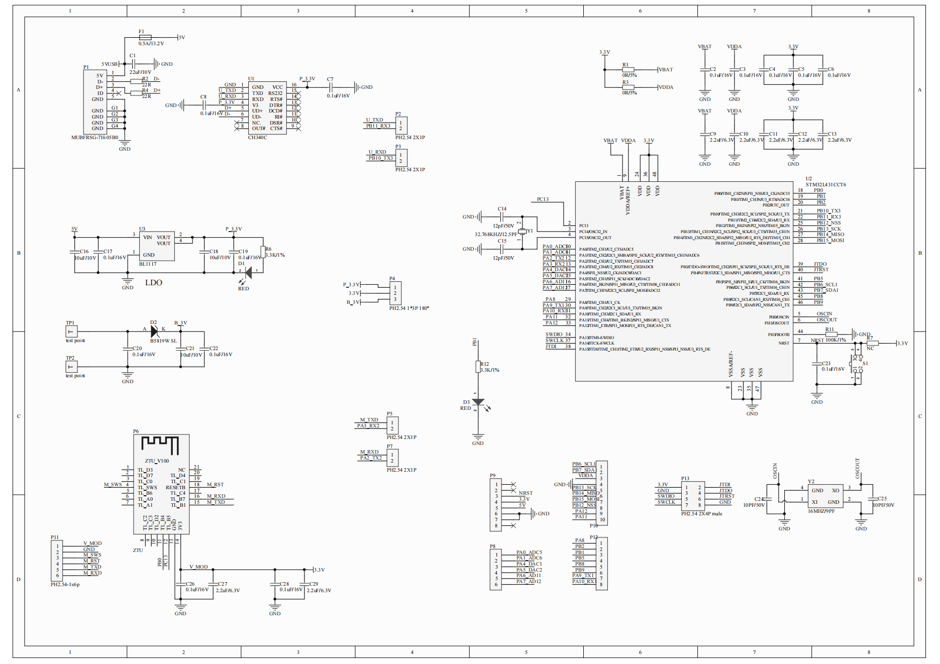
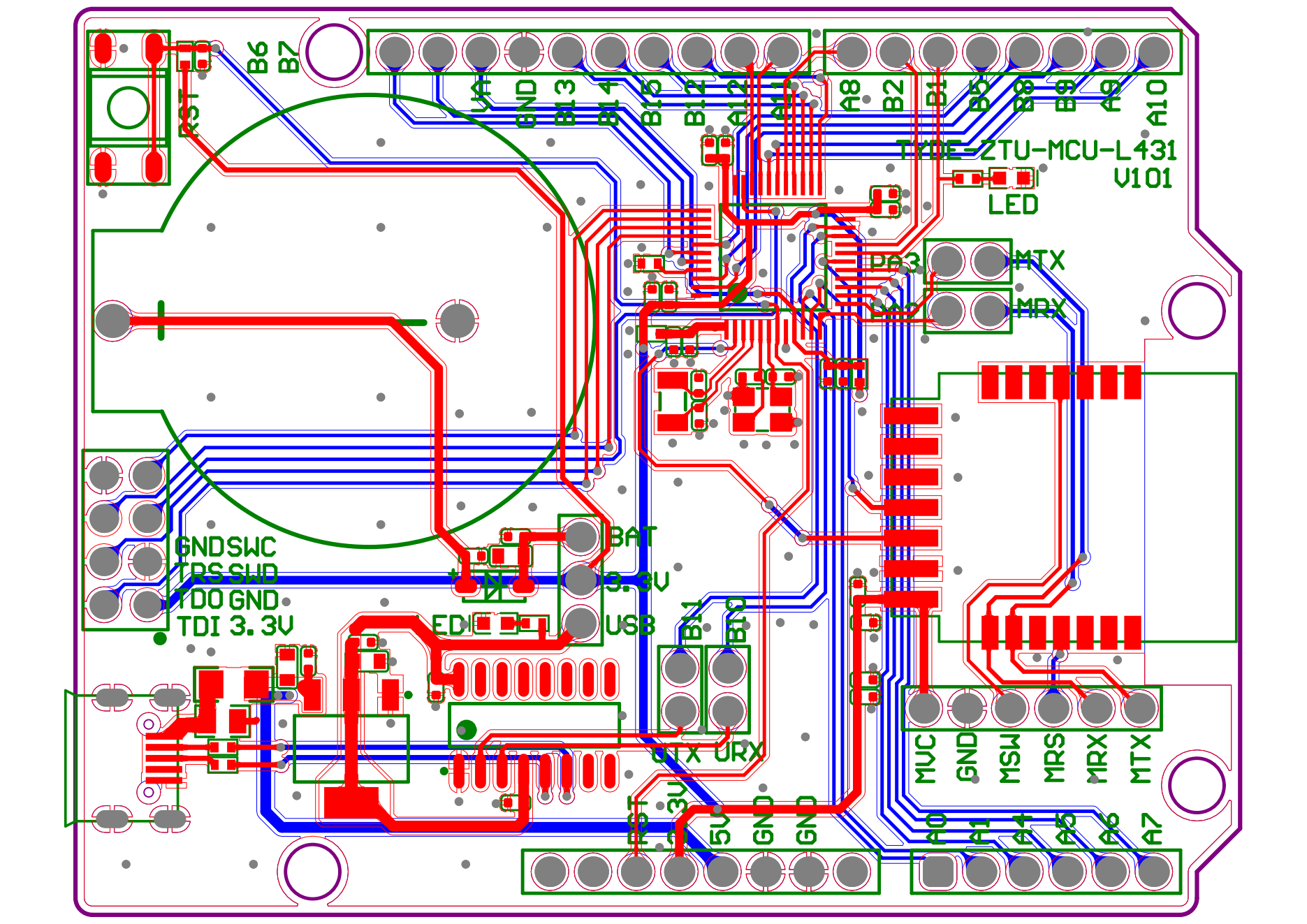
Schematic diagram and PCB
-
The schematic diagram of the board:
-
The PCB board:
Jumper settings
-
The board has a built-in USB-to-serial chip. You can use a jumper cap on
PB10andPB11to connect the MCU to the USB-to-serial chip.Pin connection description
Silkscreen P2 P3 MCU pin PB11 PB10 USB-to-serial chip USB-TXD USB-RXD -
You can use a jumper cap on
PA2andPA3to connect the MCU to the ZTU module.Pin connection description
Silkscreen P5 P7 MCU pin PA3 PA2 ZTU module TL_B1 TL_B7 -
You can use a jumper cap to switch the power supply between the USB connection and external power supply. The following table provides the description of pin header
P4.Silkscreen Description BAT Place a jumper cap on BATand3.3Vto supply power via battery.3.3V 3.3V power output pin. USB Place a jumper cap on USBand3.3Vto supply power via USB connection.The
+and-pin headers are used to connect to a CR2450 battery.
Module connection for flashing
For flashing license and firmware, connect pins following the table and figure shown below.
| Microcontroller board | Pin header P11 | Module pin | Connector |
|---|---|---|---|
| Zigbee ST(L4) Board (ZTU) | MVC | 3V3 | Connect the Telink writer to UART with jumper wires |
| GND | GND | ||
| MSW | TL_SWS | ||
| MRS | RESETB | ||
| MRX | TL_B1 | ||
| MTX | TL_B7 |
USB-to-serial chip driver
Download the USB-to-serial chip driver for your operating system.
Things to note
- The board has a built-in micro-USB port, so the additional power board is not necessary.
- If you connect the board to a power board, do not use the micro-USB port for voltage input.
Is this page helpful?
YesFeedbackIs this page helpful?
YesFeedback


