Wi-Fi & Bluetooth LE SoC NANO (BK7231N)
The Tuya Sandwich Wi-Fi and Bluetooth LE combo SoC NANO has BK7231N chip as a microcontroller, which is designed to help you easily prototype your IoT ideas. It can work with functional boards or circuit boards to implement specific features.
Applications
- This development board applies to a wide range of prototypes implemented with Tuya’s no-code solutions, such as sockets, power strips, switches, and lights.
- Develop with the board to build your IoT projects easily and fast.
- You can use this board for different development purposes.
- Embedded program development and debugging
- App development and debugging
- Creating connected devices that can be controlled with a mobile phone
- Getting started with IoT development and learning how the Wi-Fi-based control system works
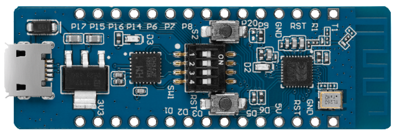
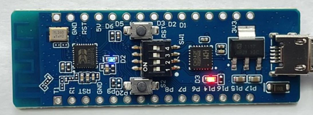
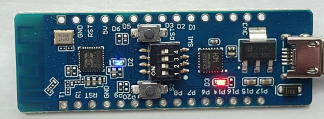
Components
The development board is integrated with the cost-effective Wi-Fi and Bluetooth LE combo chip BK7231N from Beken Corporation. It has on-board buttons, LED, GPIOs, and a USB-to-serial chip.
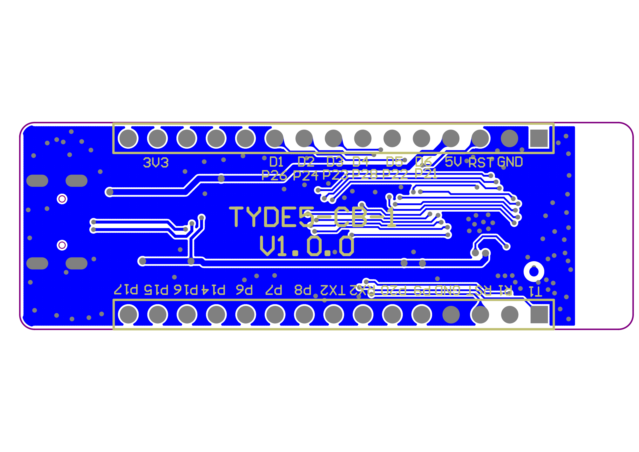
I/O port and pin description
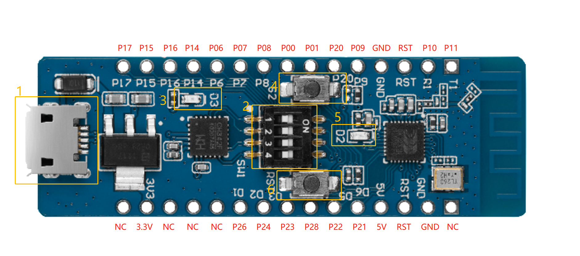
- Micro-USB (CN1): Inputs 5V DC voltage and provides two extended serial ports
- DIP switch (S1): Flip the toggle to the ON position to complete the circuit. The switch is used to open and close the circuit between the USB-to-serial chip and the chip’s serial port.
- LED indicator (D3): When the 3.3V power is on, the LED is on.
- Button (S2): When the button is pressed, P9 outputs low. When the button is released, it outputs high.
- LED indicator (D2): When P16 outputs low, the LED is on.
- Button (RST): When the button is pressed, P9 outputs low. When the button is released, it outputs high.
-
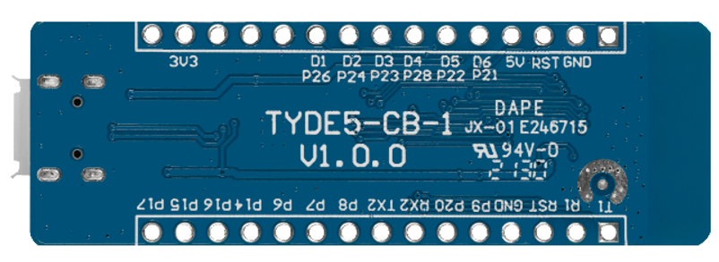
Pin description
No. Pin name Description 1 NC Leave it floating. 2 3.3V 3.3V power pin. 3 NC Leave it floating. 4 NC Leave it floating. 5 NC Leave it floating. 6 P26 GPIOP_26on BK7231N, which can be reused as the PWM5.7 P24 GPIOP_24on BK7231N, which can be reused as the PWM4.8 P23 GPIOP_23on BK7231N, which can be reused as the ADC.9 P28 GPIOP_28on BK7231N.10 P22 GPIOP_22on BK7231N.11 P21 GPIOP_21on BK7231N, which can be reused as the I2C1 SDA.12 5V 5V power pin. 13 RST Clock enable (CEN) pin on BK7231N. It can output the chip enable and high enable signals. 14 GND Ground pin. 15 NC Leave it floating. 16 P11 GPIOP_11on BK7231N, which can be reused as the UART1 TXD pin and generally used as the user I/O.17 P10 GPIOP_10on BK7231N, which can be reused as the UART1 RXD pin and generally used as the user I/O.18 RST Clock enable (CEN) pin on BK7231N. It can output the chip enable and high enable signals. 19 GND Ground pin. 20 P09 GPIOP_09on BK7231N, which can be reused as the PWM3.21 P20 GPIOP_20on BK7231N, which can be reused as the I2C1 SCL.22 P01 GPIOP_01on BK7231N, which can be reused as the UART2 RXD pin, generally used for log printing.23 P00 GPIOP_00on BK7231N, which can be reused as the UART2 TXD pin, generally used for log printing.24 P08 GPIOP_08on BK7231N, which can be reused as the PWM2.25 P07 GPIOP_07on BK7231N, which can be reused as the PWM1.26 P06 GPIOP_06on BK7231N, which can be reused as the PWM0.27 P14 GPIOP_14on BK7231N, which can be reused as the SPI SCK.28 P16 GPIOP_16on BK7231N, which can be reused as the SPI MOSI.29 P15 GPIOP_15on BK7231N, which can be reused as the SPI CSN.30 P17 GPIOP_17on BK7231N, which can be reused as the SPI MISO.
Load-carrying capacity
-
When micro-USB (CN1) inputs 5V DC voltage, the board can supply power to external components.
Power pin Rated voltage/current 5V Depends on the input current of the adapter connected to the DC-005 terminal. 3.3V 3.3V/0.6A -
Characteristics of output voltage
Output current 0A 0.15A 0.3A 0.45A 0.6A 0.75A Output voltage 3.34V 3.36V 3.37V 3.37V 3.38V 3.38V Note: We tested the voltage under the condition that there is no output voltage on the micro-USB (CN1) terminal.
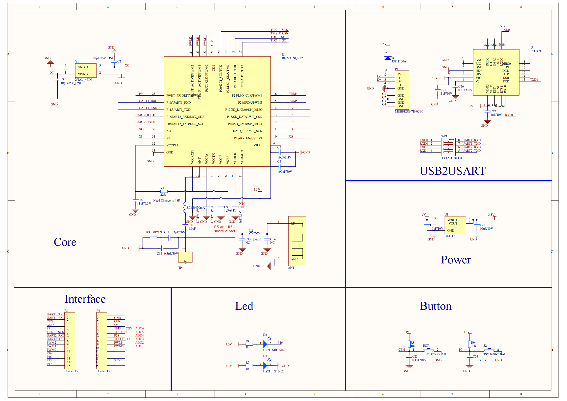
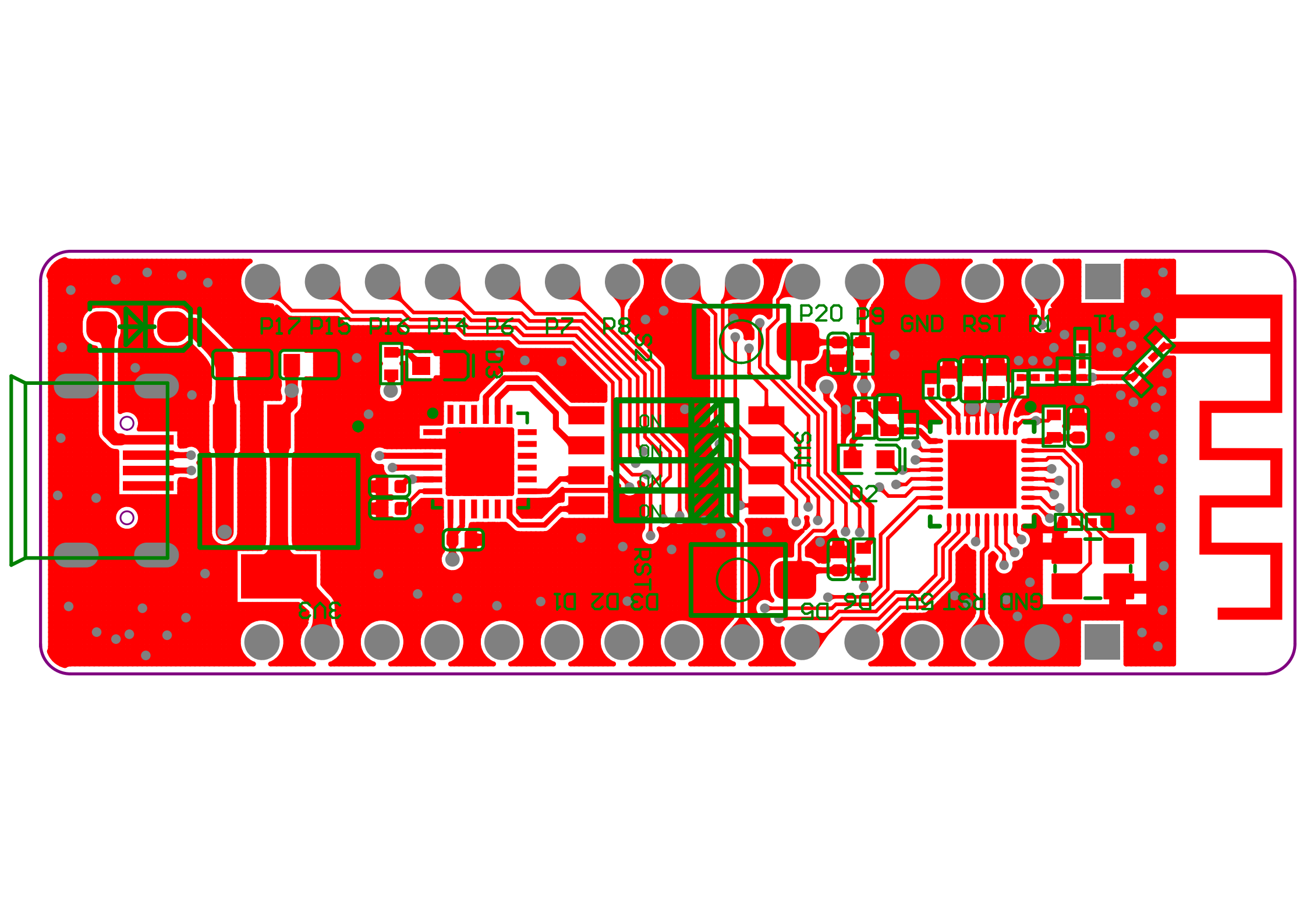
Schematic diagram and PCB
-
The schematic diagram of the board:
-
The PCB board:
How USB-to-serial works
-
The board has a built-in USB-to-serial chip. The single-channel USB port can provide two extended serial ports. You can flip the DIP switch (S1) to enable the 2-channel serial port on the BK7231N to connect to the USB-to-serial chip. The following table lists the pin definition of the DIP switch.
DIP switch No. 1 2 3 4 BK7231N chip UART1_RX UART1_TX UART2_RX UART2_TX USB-to-serial chip USB-TX0 USB-RX0 USB-TX1 USB-RX1
Note:
- Flip the toggle to the ON position to complete the circuit. The switch is used to open and close the circuit between the USB-to-serial chip and the chip’s serial port.
- When you use the UART pin on the chip for communication with an MCU or GPIO, flip the toggle of the corresponding channel to the OFF position (the side with numbers) to open the circuit between the UART on BK7231N and the USB-to-serial chip.
-
The COM ports map to the UART pins as follows.
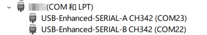
COM ports on the computer SERIAL-A(COM23) SERIAL-B(COM22) USB-to-serial chip USB-UART0 USB-UART1 BK7231N chip UART1 UART2
Note: The COM port number varies depending on computers so we use
SERIAL-AandSERIAL-Bto indicate the two COM ports.
Connection for DOWNLOAD mode
Flip the toggles of channel 1 and 2 on the DIP switch (S2) to the ON position to complete the circuit between the UART1 on BK7231N and the host.
Connection for viewing logs on the host
Flip the toggles of channel 3 and 4 on the DIP switch (S2) to the ON position to complete the circuit between the UART2 on BK7231N and the host.
Connection for user I/O and host communication
Flip the toggles of channel 1 and 2 on the DIP switch (S2) to the ON position to complete the circuit between the UART1 on BK7231N and the host.
Connection for using both UARTs as GPIOs
Flip the toggles of channel 1 to 4 on the DIP switch (S2) to the OFF position to open the circuit between the UARTs on BK7231N and the USB-to-serial chip.
USB-to-serial chip driver
Download the USB-to-serial chip driver for your operating system.
Things to note
- The board has a built-in power supply port and circuit, so the additional power board is not necessary.
- This board only supports USB port that supplies 5V output.
- If you want to use P10, P11, P00, and P01 for other circuits, make sure to flip the toggle of the corresponding channel to the OFF position to open the circuit between the UART on BK7231N and the USB-to-serial chip.
Is this page helpful?
YesFeedbackIs this page helpful?
YesFeedback


