Wi-Fi & Bluetooth LE SoC NANO (WBRU)
The Tuya Sandwich Wi-Fi and Bluetooth Low Energy (LE) combo SoC has Tuya’s WBRU network module as a microcontroller, which is designed to help you easily prototype your IoT ideas. It can work with functional boards or circuit boards to implement specific features.
Applications
- This development board applies to a wide range of prototypes implemented with Tuya’s no-code solutions, such as sockets, power strips, switches, and lights.
- Develop with the board to build your IoT projects easily and fast.
- You can use this board for different development purposes.
- Embedded program development and debugging
- App development and debugging
- Creating connected devices that can be controlled with a mobile phone
- Getting started with IoT development and learning how the Wi-Fi-based control system works
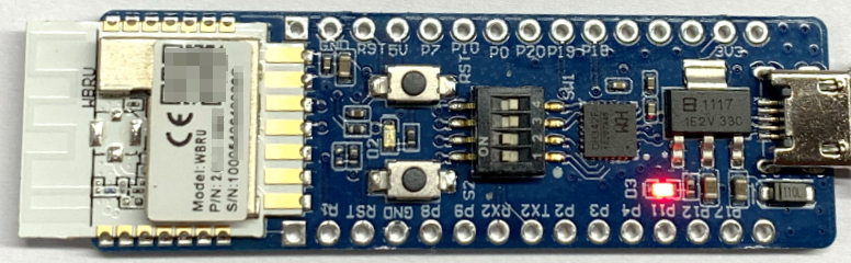
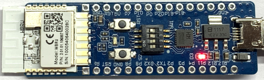
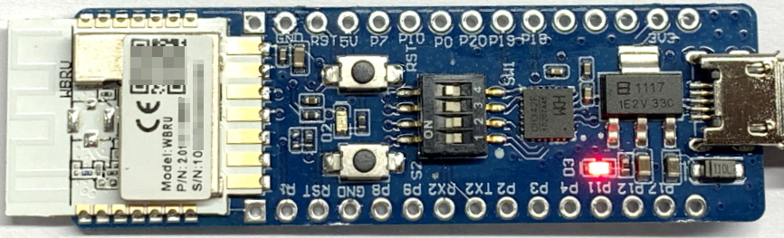
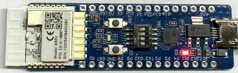
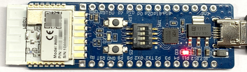
Components
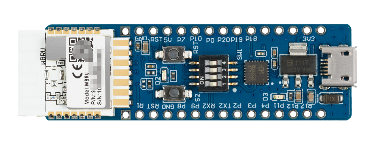
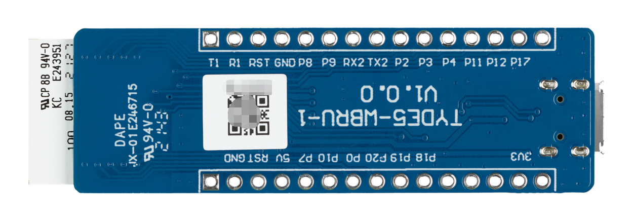
The development board is integrated with Tuya’s proprietary low-power Wi-Fi and Bluetooth LE combo module WBRU. This module consists of a highly integrated wireless chip W701-VA2-CG with built-in Wi-Fi stacks and various library functions. The development board has on-board buttons, LED, GPIOs, and a USB-to-serial chip. For more information, see the WBRU Module Datasheet.
I/O port and pin description
-
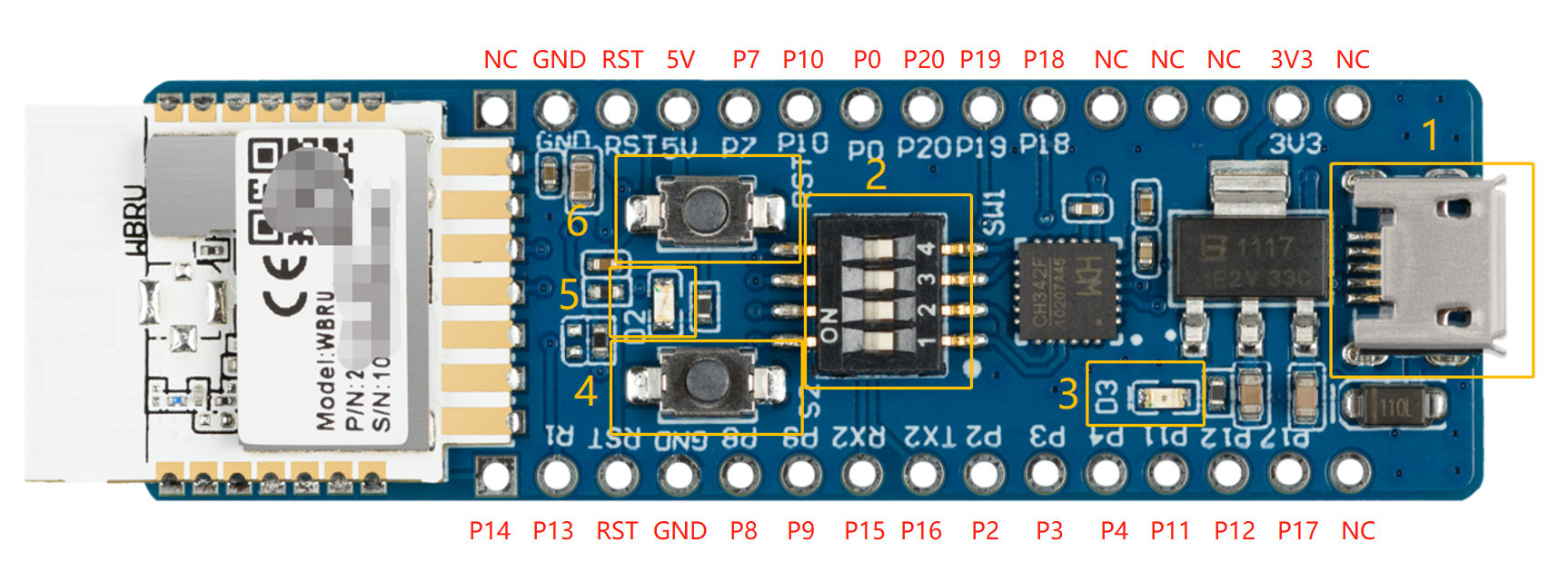
1: Micro-USB (CN1): Inputs 5V DC voltage and provides two extended serial ports.
-
2: DIP switch (S1): Flip the toggle to the ON position to complete the circuit. The switch is used to open and close the circuit between the USB-to-serial chip and the chip’s serial port.
-
3: LED indicator (D3): When the 3.3V power is on, the LED is on.
-
4: Button (S2): When the button is pressed, PA12 outputs low. When the button is released, it outputs high.
-
5: LED indicator (D2): When PA18 outputs low, the LED is on.
-
6: Button (RST): When the button is pressed, the module is reset.
Pin description
No. Pin name Description 1 NC Leave it floating. 2 3.3V 3.3V power pin. 3 NC Leave it floating. 4 NC Leave it floating. 5 NC Leave it floating. 6 PA18 GPIOA_18on WBRU, which can be used as PWM output.7 PA19 GPIOA_19on WBRU, which can be used as PWM output.8 PA20 GPIOA_20on WBRU, a GPIO pin.9 PA0 GPIOA_0on WBRU. Pull-up will trigger the testing mode. It is not recommended to add an external pull-up resistor for this pin.10 PA10 GPIOA_10on WBRU, which can be reused asSPI_MISO.11 PA7 GPIOA_7on WBRU, which can be reused asSPI_CS.12 5V 5V power pin. 13 RST Clock enable (CEN) pin on WBRU. It can output the chip enable and high enable signals. 14 GND Ground pin. 15 NC Leave it floating. 16 PA14 GPIOA_14on WBRU, which can be reused as theUART0_TXDpin for serial communication.17 PA13 GPIOA_13on WBRU, which can be reused as theUART0_RXDpin for serial communication.18 RST Clock enable (CEN) pin on WBRU. It can output the high enable signal. 19 GND Ground pin. 20 PA8 GPIOA_8on WBRU, which can be reused asSPI_SCK.21 PA9 GPIOA_9on WBRU, which can be reused asSPI_MOSI.22 PA15 GPIOA_15on WBRU, which can be reused as theUART_Log_RXDpin for log printing.23 PA16 GPIOA_16on WBRU, which can be reused as theUART_Log_TXDpin for log printing.24 PA2 GPIOA_2on WBRU, which can be used as PWM output.25 PA3 GPIOA_3on WBRU, which can be used as PWM output.26 PA4 GPIOA_4on WBRU, which can be used as PWM output.27 PA11 GPIOA_11on WBRU, which can be used as PWM output.28 PA12 GPIOA_12on WBRU, which can be used as PWM output.29 PA17 GPIOA_17on WBRU, which can be used as PWM output.30 NC Leave it floating.
Load-carrying capacity
-
When micro-USB (CN1) inputs 5V DC voltage, the board can supply power to external components.
Power pin Rated voltage/current 5V Depends on the input current of the adapter connected to the DC-005 terminal. 3.3V 3.3V/0.6A -
Characteristics of output voltage
Output current 0A 0.15A 0.3A 0.45A 0.6A 0.75A Output voltage 3.34V 3.36V 3.37V 3.37V 3.38V 3.38V We tested the voltage under the condition that there is no output voltage on the micro-USB (CN1) terminal.
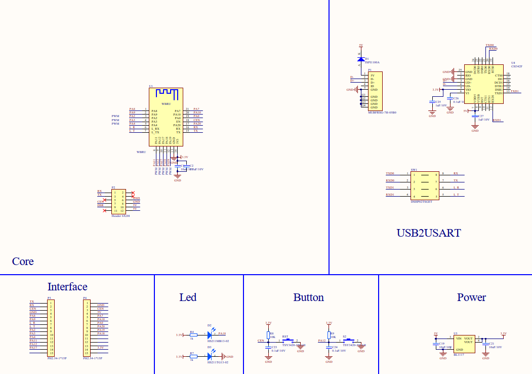
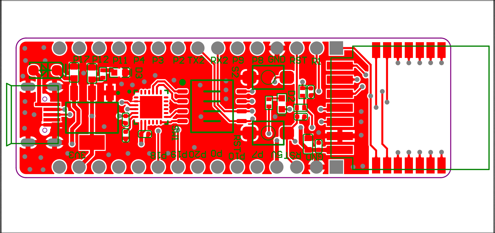
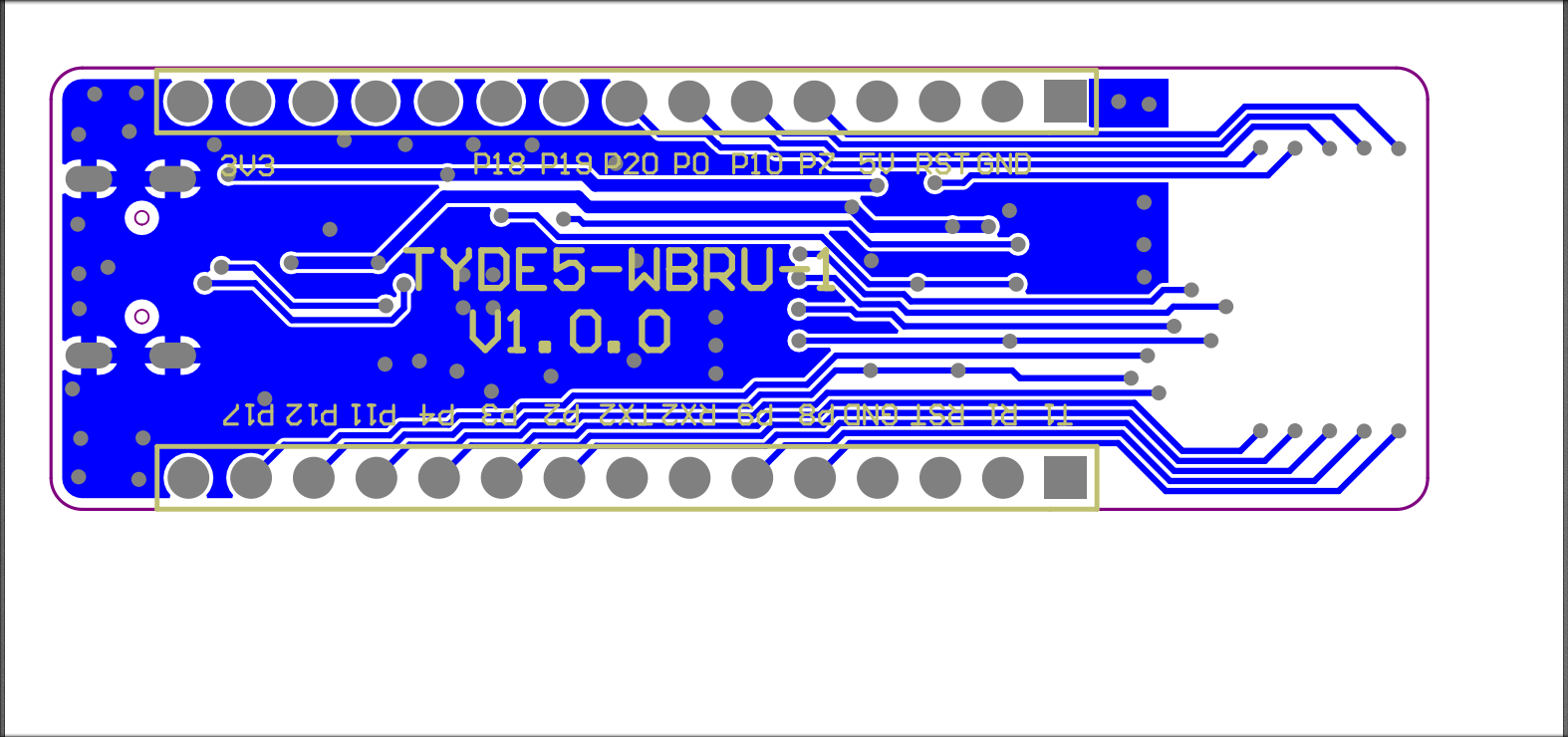
Schematic diagram and PCB
-
The schematic diagram of the board:
-
The PCB board:
How USB-to-serial works
-
The board has a built-in USB-to-serial chip. The single-channel USB port can provide two extended serial ports. You can flip the DIP switch (SW1) to enable the 2-channel serial port on the WBRU to connect to the USB-to-serial chip. The following table lists the pin definition of the DIP switch.
DIP switch No. 1 2 3 4 WBRU module UART1_RX UART1_TX UART2_RX UART2_TX USB-to-serial chip USB-TX0 USB-RX0 USB-TX1 USB-RX1 - Flip the toggle to the ON position to complete the circuit. The switch is used to open and close the circuit between the USB-to-serial chip and the chip’s serial port.
- When you use the UART pin on the chip for communication with an MCU or GPIO, flip the toggle of the corresponding channel to the OFF position (the side with numbers) to open the circuit between the UART on WBRU and the USB-to-serial chip.
-
The COM ports map to the UART pins as follows.
COM ports on the computer SERIAL-A(COM23) SERIAL-B(COM22) USB-to-serial chip USB-UART0 USB-UART1 WBRU module UART1 UART2 The COM port number varies depending on computers so we use
SERIAL-AandSERIAL-Bto indicate the two COM ports.
Connection for DOWNLOAD mode
-
If you use Tuya’s software for firmware flashing and module authorization, flip the toggles of channels 1 and 2 on the DIP switch (SW1) to the ON position to complete the circuit between the UART1 on WBRU and the host.
The development board comes with pre-flashed firmware. In this mode, pre-flashed firmware is run.
-
If you use the chip manufacturer’s software for firmware flashing, flip the toggles of channels 3 and 4 on the DIP switch (SW1) to the ON position to complete the circuit between the UART2 on WBRU and the host. Connect PA0 and PA13 to the 3.3V pin.
The chip manufacturer’s software can only be used to flash firmware to the module. You need to use Tuya’s software to authorize the module.
If you flash the firmware to the module at a specified address, authorizing the module again is not needed.
Connection for viewing logs on the host
Flip the toggles of channel 3 and 4 on the DIP switch (SW1) to the ON position to complete the circuit between the UART2 on WBRU and the host.
Connection for user I/O and host communication
Flip the toggles of channel 1 and 2 on the DIP switch (SW1) to the ON position to complete the circuit between the UART1 on WBRU and the host.
Connection for using both UARTs as GPIOs
Flip the toggles of channel 1 to 4 on the DIP switch (SW1) to the OFF position to open the circuit between the UARTs on WBRU and the USB-to-serial chip.
USB-to-serial chip driver
Download the USB-to-serial chip driver for your operating system.
Things to note
- The board has a built-in power supply port and circuit, so the additional power board is not necessary.
- This board only supports USB port that supplies 5V output.
- If you want to use PA13, PA14, PA15, and PA16 for other circuits, make sure to flip the toggle of the corresponding channel to the OFF position to open the circuit between the UART on WBRU and the USB-to-serial chip.
Is this page helpful?
YesFeedbackIs this page helpful?
YesFeedback


