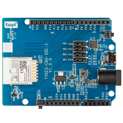
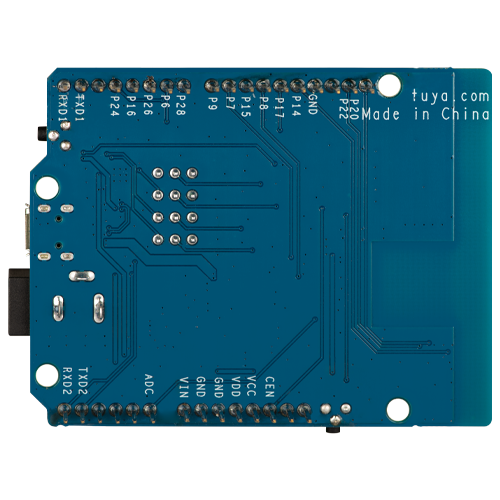
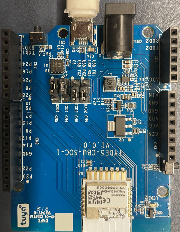
Wi-Fi and Bluetooth LE SoC Board (CBU)
The Tuya Sandwich Wi-Fi and Bluetooth LE combo SoC has Tuya’s CBU network module as a microcontroller, which is designed to help you easily prototype your IoT ideas. It can work with functional boards or circuit boards to implement specific features.
Applications
- This development board applies to a wide range of prototypes implemented with Tuya’s no-code solutions, such as sockets, power strips, switches, and lights.
- Develop with the board to build your IoT projects easily and fast.
- You can use this board for different development purposes.
- Embedded program development and debugging
- App development and debugging
- Creating connected devices that can be controlled with a mobile phone
- Getting started with IoT development and learning how the Wi-Fi-based control system works
Components
The development board is integrated with Tuya’s proprietary high-performance Wi-Fi and Bluetooth LE combo module. It has on-board buttons, LED, GPIOs, and a USB-to-serial chip. For more information, see the CBU Module Datasheet.
I/O port and pin description
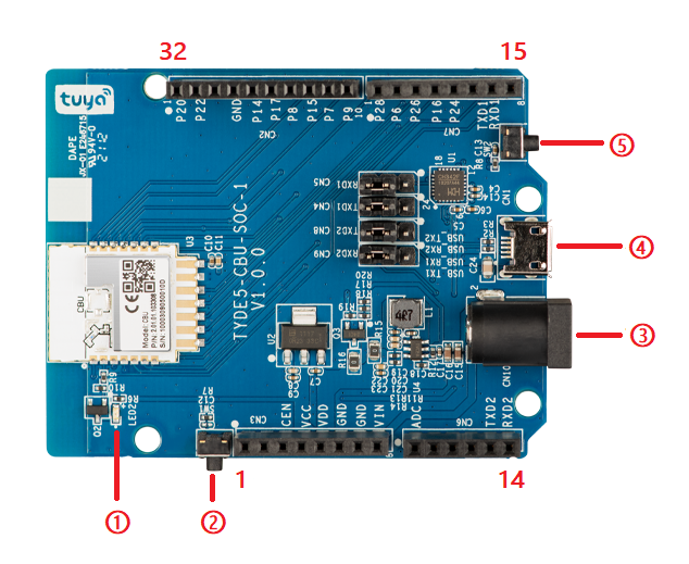
-
1: LED indicator (LED2): When P16 outputs high, the LED is on.
-
2: Button (SW1): When the button is pressed, P28 outputs low. When the button is released, it outputs high.
-
3: DC-005 (CN5): Inputs 12V DC voltage.
-
4: Micro-USB (CN1): Inputs 5V DC voltage and provides two extended serial ports.
-
5: Button (SW1): Module’s enable pin that is active low. When the button is pressed, the pin outputs low.
-
Pin description
No. Pin name Function 1 NC Leave it floating. 2 NC Leave it floating. 3 CEN Module’s enable pin that is active low. 4 VCC 3.3V power pin. 5 VDD 5V power pin. 6 GND Ground pin. 7 GND Ground pin. 8 VIN 12V power pin. 9 ADC P23 on the module. It can be reused as ADC. 10 NC Leave it floating. 11 NC Leave it floating. 12 NC Leave it floating. 13 TXD2 You can use a jumper cap to switch to UART_TX2on the module.UART_TX2supports log printing, corresponding to P0 on the IC. You can also use a jumper cap to leave TXD2 floating.14 RXD2 You can use a jumper cap to switch to UART_RX2on the module.UART_RX2corresponds to P1 on the IC. Do not use P1. You can also use a jumper cap to leave RXD2 floating.15 RXD1 You can use a jumper cap to switch to UART_RX1on the module.UART_RX1receives user data, corresponding to P10 on the IC. You can also use a jumper cap to leave RXD1 floating.16 TXD1 You can use a jumper cap to switch to UART_TX1on the module.UART_TX1sends user data, corresponding to P11 on the IC. You can also use a jumper cap to leave TXD1 floating.17 NC Leave it floating. 18 P24 P24 on the module. A normal GPIO that can be reused as hardware PWM4. 19 P16 P16 on the module. A normal GPIO that can be reused as SPI_MOSI.20 P26 P26 on the module. A normal GPIO that can be reused as hardware PWM5. 21 P06 P6 on the module. A normal GPIO that can be reused as hardware PWM0. 22 P28 P28 on the module. A normal GPIO. 23 P09 P9 on the module. A normal GPIO that can be reused as hardware PWM3. 24 P07 P7 on the module. A normal GPIO that can be reused as hardware PWM1. 25 P15 P15 on the module. A normal GPIO that can be reused as SPI_CS.26 P08 P8 on the module. A normal GPIO that can be reused as hardware PWM2. 27 P17 P17 on the module. A normal GPIO that can be reused as SPI_MISO.28 P14 P14 on the module. A normal GPIO that can be reused as SPI_SCK.29 GND Ground pin. 30 NC Leave it floating. 31 P22 P22 on the module. A normal GPIO. 32 P20 P20 on the module. A normal GPIO.
Load-carrying capacity
-
When DC-005 inputs 12V DC voltage, the board can supply power to external components.
Power pin Rated voltage/current VIN Depends on the input current of the adapter connected to the DC-005 terminal. VDD 5V/1A VCC 3.3V/0.6A This board outputs rated power of 5W, which cannot support the long-time simultaneous output of 5V/1A and 3.3V/0.6A.
-
Characteristics of the output voltage of VDD
Output current 0A 0.25A 0.5A 0.75A 1A 1.25A Output voltage 5.01V 5.00V 4.99V 4.98V 4.98V 4.97V We tested the voltage under the condition that there is no output voltage on VCC.
-
Characteristics of output voltage
Output current 0A 0.15A 0.3A 0.45A 0.6A 0.75A Output voltage 3.34V 3.36V 3.37V 3.37V 3.38V 3.38V We tested the voltage under the condition that there is no output voltage on VDD.
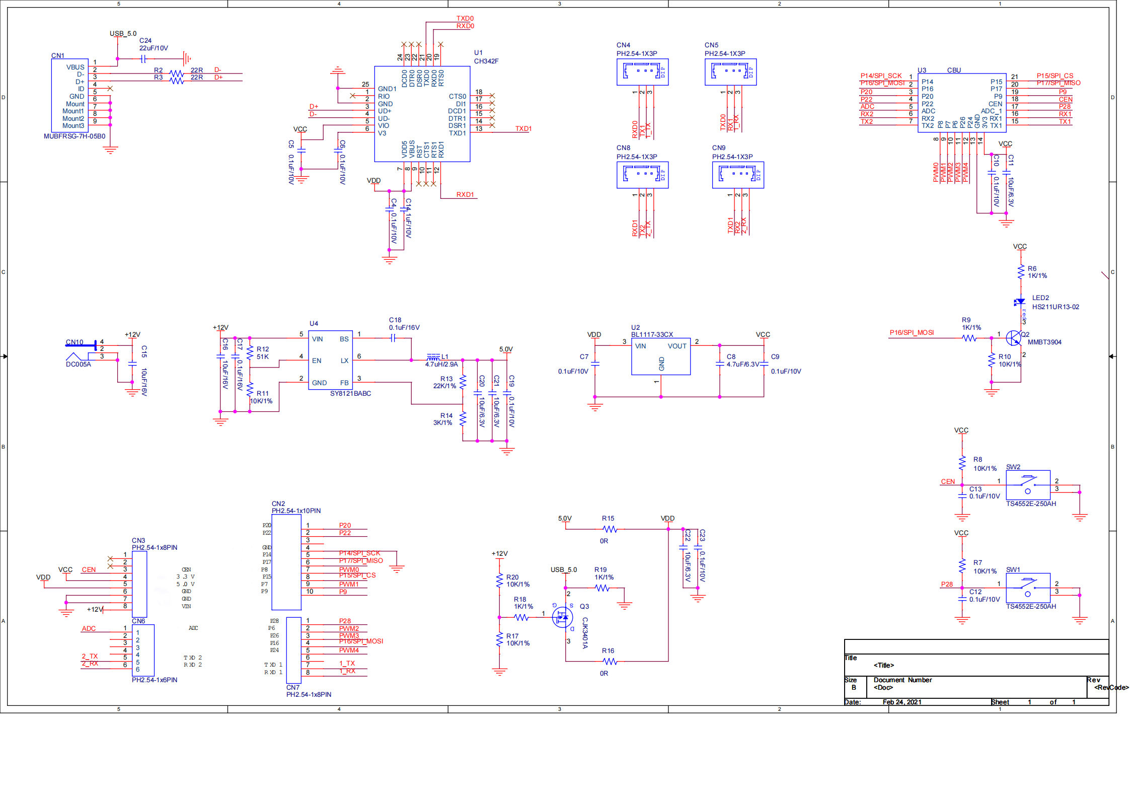
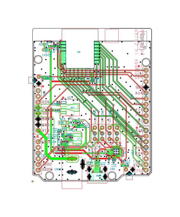
Schematic diagram and PCB
-
The schematic diagram of the board:
-
The PCB board:
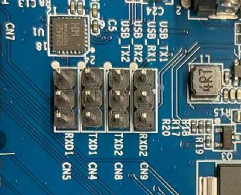
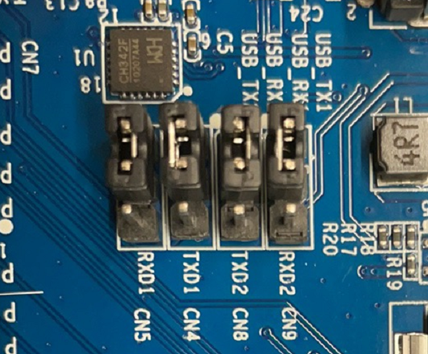
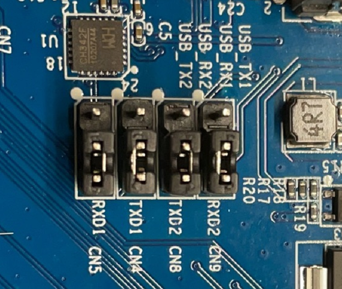
How USB-to-serial chip works
-
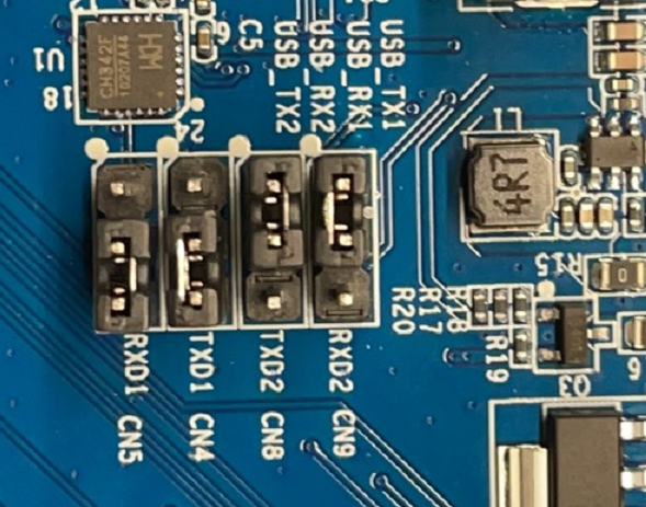
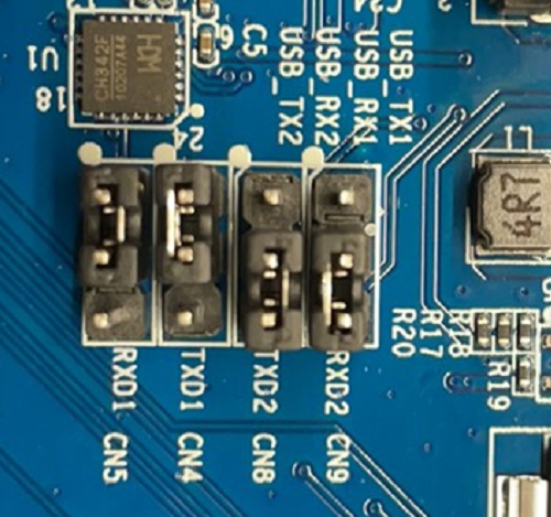
The board has a built-in USB-to-serial chip. The single-channel USB port can provide two extended serial ports. You can use a jumper cap to allow the 2-channel serial port on the module to connect to the USB-to-serial chip. Pin connection description
Silkscreen of pin header CN9 CN8 CN4 CN5 Pins on module UART_RX2 UART_TX2 UART_TX1 UART_RX1 Pins on board RXD2 TXD2 TXD1 RXD1 Pins on USB-to-serial chip USB-TX1 USB-RX1 USB-RX2 USB-TX2 -
The serial port is left floating and not connected to the pins on the USB-to-serial chip or the board. The four headers are open without jumper caps.
-
The two serial ports on the module are connected to the USB-to-serial chip. The RXD2, TXD2, TXD1, and RXD1 on the board are left floating. Put the jumper caps as shown below.
-
The two serial ports on the module are connected to the pins on the board. The pins on the USB-to-serial chip are left floating. Put the jumper caps as shown below.
-
Connect UART1 (user serial) to the pins on the board, UART2 (log printing) to the USB-TX1 and USB-RX1. Put the jumper caps as shown below.
-
Connect UART1 (user serial) to USB-TX2 and USB-RX2, UART2 (log printing) to pins on the board. Put the jumper caps as shown below.
Connection for flashing
For flashing license and firmware, connect pins following the table and figure shown below.
| Board | Pins on module | Pins on USB-to-serial chip | Connector |
|---|---|---|---|
| Tuya Sandwich Wi-Fi and Bluetooth LE combo SoC (CBU) | 3.3V | 3.3V | Micro-USB cable |
| UART_TX1 | USB-RX2 | ||
| UART_RX1 | USB-TX2 | ||
| GND | GND |
USB-to-serial chip driver
Download the USB-to-serial chip driver for your operating system.
Things to note
- The board has a built-in power supply port and circuit, so the additional power board is not necessary.
- You can connect the USB port (5V) or DC005 port (12V) to a power supply. Note that the DC005 port does not support input voltage less than 7V.
- If you connect the board to a power board, do not use the DC005 port for voltage input.
Is this page helpful?
YesFeedbackIs this page helpful?
YesFeedback


