Tuya Sandwich Zigbee SoC Board (ZS3L)
The Tuya Sandwich Zigbee SoC master control board (ZS3L) helps you quickly implement various smart hardware prototypes. You can use the Tuya Zigbee SoC master control board (ZS3L) with other functional circuit modules or circuit boards to implement corresponding functions.
Scenarios
-
The Tuya Sandwich Zigbee SoC master control board (ZS3L) applies to many prototypes developed by Tuya IoT plug and play solutions, including sockets, power strips, and switches.
-
You also can implement diversified smart hardware demos with this development board.
-
The common scenarios of the Tuya Sandwich Zigbee master control board (ZS3L) are as follows:
- Embedded systems engineers can use the board to perform preliminary embedded programming and debugging.
- App developers can use the board to develop and debug apps.
- Makers can use the board to quickly implement hardware demos and device control with the mobile phone.
- IoT technology enthusiasts can use the board to learn about the Zigbee control principle and smart device development.
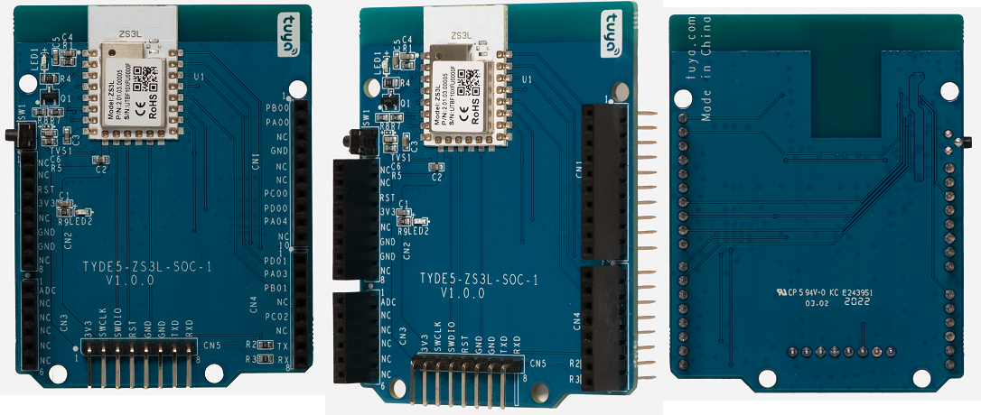
Introduction to key components
The Tuya Sandwich Zigbee SoC master control board (ZS3L) adopts the high-performance Zigbee module ZS3L developed by Tuya Smart. The development board contains Zigbee module ZS3L, buttons, LED indicators, user-defined I/O interfaces, power supply, and more. For more information, see ZS3L Module Datasheet.
I/O ports and function definitions
-
CN5 serial port for UART upgrade: Used for system upgrade and debugging.
-
LED indicator LED1: You can customize its functions. The indicator is controlled by PD00 and is active high.
-
LED indicator LED2: 3.3V power indicator.
-
Button SW1: You can customize its functions. The button is detected by PD01. Its logic level is high when initialized and is low when pressed.
-
Other GPIO ports: You can customize their functions. See the following table.
No. Symbol Description 1 RST The hardware reset pin. Its default logic level is high. It is active when pulled down. 2 3V3 3.3V power input pin. 3 GND Power ground. 4 ADC ADC port. 12-bit SAR analog-to-digital converter. 5 RX UART_RXD. 6 TX UART_TXD. 7 PC02 GPIO. It can be configured as PWM output pin. 8 PB01 GPIO. It can be configured as PWM output pin. 9 PA03 GPIO. It can be configured as PWM output pin. 10 PD01 GPIO. It can be configured as PWM output pin. 11 PA04 GPIO. It can be configured as PWM output pin. 12 PD00 GPIO. It can be configured as PWM output pin. 13 PC00 GPIO. It can be configured as PWM output pin. 14 PA00 GPIO. It can be configured as PWM output pin. 15 PB00 GPIO. It can be configured as PWM output pin.
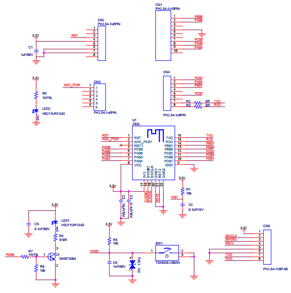
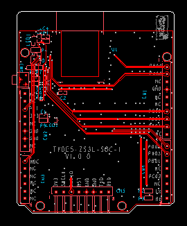
Schematic diagram and PCB
-
Schematic diagram of Tuya Sandwich Zigbee SoC master control board (ZS3L):
-
PCB of Tuya Sandwich Zigbee SoC master control board (ZS3L):
Things to note
- The development board in this solution must be used with a power board.
- The development board in this solution only supports 3.3V power input, and the supply current is not less than 350mA.
Is this page helpful?
YesFeedbackIs this page helpful?
YesFeedback


