Tuya Smart Wi-Fi Module--WR5P
Product Overview
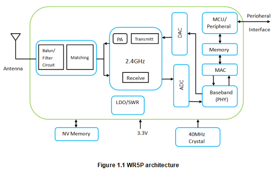
WR5P is a low power-consuming built-in Wi-Fi module developed by Hangzhou Tuya Information Technology Co., Ltd. It consists of a highly integrated wireless radio chip (RTL8710BN) and an external flash chip, with a built-in Wi-Fi network protocol stack and robust library functions. WR5P also contains a low power-consuming ARM CM4F, a WLAN MAC, a 1T1R WLAN, a basic frequency of up to 125 MHz, a 256 KB SRAM, a 1 MB flash, and various peripheral resources.
WR5P is an RTOS platform that integrates all the function libraries of the Wi-Fi MAC and TCP/IP protocols. You can develop built-in Wi-Fi products as required.
Figure 1.1 shows the architecture of WR5P.
Features
Built-in low power-consuming 32-bit CPU, which can also be used as an application processor
- Basic frequency: 125 MHz
Working voltage:3 V to 3.6 V
Peripherals: nine GPIOs, one UART, and one ADC
Wi-Fi connectivity
-
802.11 B/G/N20/N40
-
Channel 1–14@2.4 GHz
-
WPA/WPA2 security mode supported
-
+20 dBm output power in 802.11b mode
-
SmartConfig function supported (for Android and iOS devices)
-
Onboard PCB antenna
-
Certified by CE, FCC, and SRRC
-
Working temperature: –20°C to +85°C
Major Application Fields
- Intelligent building
- Intelligent home and household applications
- Health care
- Industrial wireless control
- Baby monitor
- Network camera
- Intelligent bus
Module Interfaces
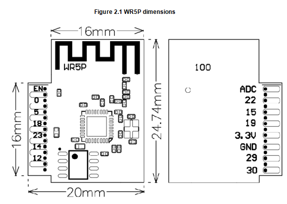
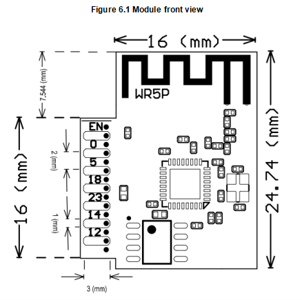
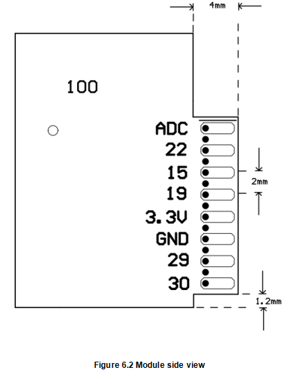
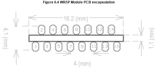
Dimensions and Footprint
WR5P provides two rows of pins with the distance of 2.0 mm between every two pins.
WR5P dimensions: 16 mm (W) x 24.74 mm (L) x 3.3 mm (H) (see figure 2.1)
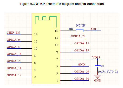
Pin Definition
Table 2.1 describes the common pins.
Table 2.1 WR5P pins
| Pin | Symbol | I/O Type | Functions |
|---|---|---|---|
| 1 | GPIOA_30 | I/O | UART_Log_TXD (used for printing of the module internal information) |
| 2 | GPIOA_12 | I/O | GPIOA_12 |
| 3 | GPIOA_29 | I/O | UART_Log_RXD (used for printing of the module internal information) |
| 4 | GPIOA_14 | I/O | GPIOA_14 |
| 5 | GND | P | Power supply reference ground pin |
| 6 | GPIOA_23 | I/O | UART0_TXD (user’s serial port) |
| 7 | VD33 | P | Module power supply pin (3.3 V) |
| 8 | GPIOA_18 | I/O | UART0_RXD (user’s serial port) |
| 9 | GPIOA_19 | I/O | GPIOA_19 |
| 10 | GPIOA_5 | I/O | GPIOA_5 |
| 11 | GPIOA_15 | I/O | GPIOA_15 |
| 12 | GPIOA_0 | I/O | GPIOA_0, which cannot be pulled up during power-on and can be configured after power-on |
| 13 | GPIOA_22 | I/O | GPIOA_22 |
| 14 | EN | I/O | The pin function is disabled by firmware, user can choose not to connect. |
| 15 | ADC | AI | ADC interface, with the maximum output power of 5 V |
Note: P indicates power-supply pins, I/O indicates input/output pins, and AI indicates analog input pins.
Electrical Characteristics
Absolute Electrical Characteristics
Table 3.1 Absolute electrical characteristics
| Parameters | Description | Minimum value | Maximum value | Unit |
|---|---|---|---|---|
| Ts | Storage temperature | -40 | 105 | ℃ |
| VDD | Power supply voltage | -0.3 | 3.6 | V |
| Static electricity voltage (human model) | TAMB-25℃ | - | 2 | KV |
| Static electricity voltage (machine model) | TAMB-25℃ | - | 0.5 | KV |
Electrical conditions
Table 3.2 Normal electrical conditions
| Parameters | Description | Min | Typ | Max | Unit |
|---|---|---|---|---|---|
| Ta | Working temperature | -20 | - | 85 | ℃ |
| VDD | Working voltage | 3.0 | - | 3.6 | V |
| VIL | I/O low-level input | -0.3 | - | VCC*0.25 | V |
| VIH | I/O high-level input | VCC*0.75 | - | 3.6 | V |
| VOL | I/O low-level output | - | - | VCC*0.1 | V |
| VOH | I/O high-level output | VCC*0.8 | - | VDD | V |
| Imax | I/O drive current | - | - | 16 | mA |
| Cpad | Input pin capacitor | - | 2 | - | pF |
Wi-Fi TX Power Consumption
Table 3.3 TX power consumption during constan emission
| Symbol | Mode | Power | Typical Value | Unit |
|---|---|---|---|---|
| IRF | 11b11 Mbit/s | 17 dBm | 287 | mA |
| IRF | 11b11 Mbit/s | 18 dBm | 295 | mA |
| IRF | 11g54 Mbit/s | 15 dBm | 255 | mA |
| IRF | 11g54 Mbit/s | 17.5 dBm | 267 | mA |
| IRF | 11n BW20MCS7 | 13 dBm | 244 | mA |
| IRF | 11n BW20MCS7 | 16.5 dBm | 257 | mA |
| IRF | 11n BW40MCS7 | 13 dBm | 220 | mA |
| IRF | 11n BW40MCS7 | 16.5 dBm | 230 | mA |
Wi-Fi RX Power Consumption
Table 3.4 RX power consumption during constant emission
| Symbol | Mode | Typical Value | Unit |
|---|---|---|---|
| IRF | CPU sleep | 90 | mA |
| IRF | CPU active | 120 | mA |
Power Consumption in Operating Mode
Table 3.5 Module working current
| Working Mode | Working Status(Ta=25°C) | Typical Value | Peak Value | Unit |
|---|---|---|---|---|
| EZ mode | The module is in EZ status and the Wi-Fi indicator quickly flashes. | 115 | 130 | mA |
| Idle mode | The module is in connected status and the Wi-Fi indicator is steady on. | 50 | 110 | mA |
| Operation mode | The module is in connected status and the Wi-Fi indicator is steady on. | 120 | 265 | mA |
| Disconnection mode | The module is in disconnected status and the Wi-Fi indicator is steady off. | 35 | 90 | mA |
Note: The peak duration is about 5 µs.
The preceding parameter values vary depending on the firmware functions.
RF Features
Basic RF Features
Table 4.1,Basic RF features
| Parameter | Description |
|---|---|
| Frequency band | 2.400–2.4835 GHz |
| Wi-Fi standard | BIEEE 802.11b/g/n (channel 1–14) |
| Data transmitting rate | 11b: 1, 2, 5.5, 11 (Mbit/s) 11g: 6, 9, 12, 18, 24, 36, 48, 54 (Mbit/s) 11n: HT20 MCS0–MCS7 11n: HT40 MCS0–MCS7 |
| Antenna type | Onboard PCB antenna |
WI-FI Output Power
Table 4.2 TX power during constant emission
| Parameter | Minimum Value | Typical Value | Maximum Value | Unit | |
|---|---|---|---|---|---|
| RF average output power, 802.11b CCK mode | 11 M | - | 17.5 | - | dBm |
| RF average output power, 802.11g OFDM mode | 54 M | - | 14.5 | - | dBm |
| RF average output power, 802.11n OFDM mode | MCS7 | - | 13.5 | - | dBm |
| Frequency error | -10 | - | 10 | ppm |
WI-FI RX sensitivity
Table 4.3 RX Sensitivity
| Parameter | Minimum Value | Typical Value | Maximum Value | Unit | |
|---|---|---|---|---|---|
| PER < 8%, RX sensitivity, 802.11b CCK mode | 11 M | - | -91 | - | dBm |
| PER < 10%, RX sensitivity, 802.11g OFDM mode | 54 M | - | -75 | - | dBm |
| PER < 10%, RX sensitivity, 802.11n OFDM mode | MCS7 | - | -72 | - | dBm |
Antenna Information
Antenna types
WR5P uses the onboard PCB antenna.
Antenna Interference Reduction
To ensure optimal Wi-Fi performance when the Wi-Fi module uses the onboard PCB antenna, it is recommended that there be a space of at least 15 mm between the module antenna and other metal parts.
Packaging Information and Poduction Instructions
Mechanical Dimensions
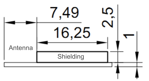
Note: PCB frame tolerance ±0.15 mm, PCB depth tolerance ±0.1 mm
Recommended PCB Encapsulation
Production Instructions
Storage conditions of a delivered module are as follows:
- The anti-moisture bag is placed in an environment where the temperature is under 30°C and the relative humidity is under 85%.
- The shelf life of a dry-packaged product is six months from the date when the product is packaged and sealed.
Precautions:
- Throughout the production process, each involved operator must wear an electrostatic ring.
- During the operation, strictly protect the module from water and strains.
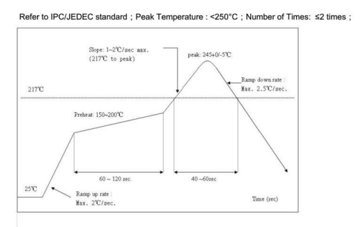
Recommended Oven Temperature Profile
Is this page helpful?
YesFeedbackIs this page helpful?
YesFeedback


