Development Board PCBA SMT Design
This topic describes the design requirements and production process control standards on printed circuit board assemblies (PCBAs) of development boards. You can reduce the potential problems respecting design and processes during production.
Scope of application
This topic is applicable to the production of PCBA clients for all development boards powered by Tuya.
References
- IPC-7527 Requirements for Solder Paste Printing
- IPC-7525B Stencil Design Guidelines
- IPC-7530A-2017 Guidelines for Temperature Profiling for Mass Soldering Processes (Reflow and Wave)
- J-STD-033 Handling, Packing, Shipping and Use of Moisture, Reflow, and Process Sensitive Devices
- IPC J-STD-001F Requirements for Soldered Electrical and Electronic Assemblies
- IPC-A-610H CN 2020 Acceptability of Electronic Assemblies
- IPC-7711C-7721C Rework, Modification and Repair of Electronic Assemblies
Suggestions on PCB design
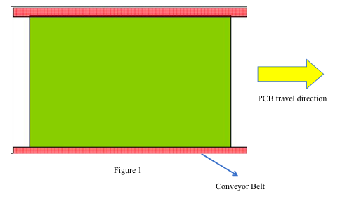
Definition of PCB travel direction
-
Along the SMT production direction, the short edge of each PCB travels through the reflow oven and its long edge is clamped on the SMT conveyor belt, as shown in Figure 1. This design helps to reduce deformation of printed circuit boards (PCBs).
-
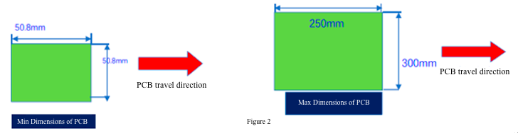
The minimum dimensions allowed for PCBs during the SMT process: L × W = 50.8 mm × 50.8 mm. If the designed dimensions are less than the required ones, panelize PCBs or increase the handling margin, as shown in Figure 2.
-
The maximum dimensions allowed for PCBs during the SMT process: L × W = 250 mm × 300 mm. The limits on the SMT capabilities are taken into account in this design, as shown in Figure 2.
Design of PCB handling margin
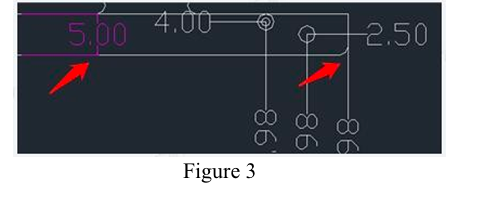
The handling margin on the conveyor belt must be 5 mm from the edge of each PCB. Do not place any components on the PCB within a distance of 5 mm from the edge. Do not include gold fingers in the handling margin. Chamfer four PCB corners, including the handling margin, as shown in Figure 3.
Design of mark points
-
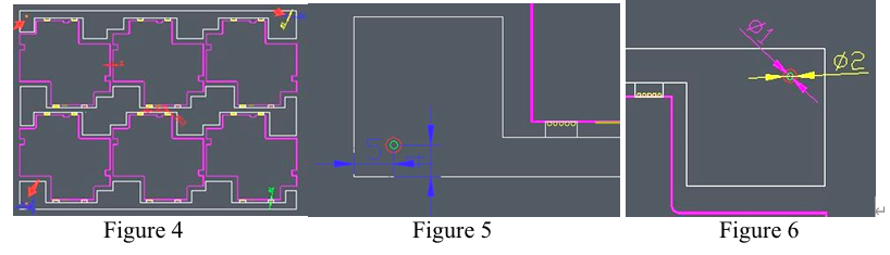
Design three or four reference points, also known as mark points, on a single surface, and arrange them asymmetrically in an L or quadrangle shape, as shown in Figure 4.
-
The center of each mark point must be 4 mm or more from the PCB edge, as shown in Figure 5.
-
If components are mounted on both faces, position mark points on both faces.
-
The outer diameter of each mark point is 2 mm. The mark point is marked as a solid circle with a diameter of 1 mm. Within the background of 2 mm in diameter, do not design pads, vias, silk screen marking, test points, or traces, as shown in Figure 6.
Suggested design of QFN thermal pad and vias
-
The vias on a quad-flat no-leads (QFN) thermal pad are recommended to be 0.2 mm in diameter. If the diameter is more than 0.3 mm, the vias must be plugged into the back to prevent the solder from flowing to the other face through the vias. When the heat dissipation precondition is met, the pitch of vias is recommended to be more than 0.8 mm. Otherwise, stencil openings might cover the vias, and thus, the thermal pad might create excessively large voids during soldering.
-
If the via diameter on a QFN thermal pad is less than 0.2 mm, do not plug the vias on both faces. Open windows in the solder mask of the thermal pad back. This way, heat can be dissipated through vias and solder bubbles can also be reduced on the thermal pad. This via diameter also prevents solder paste from penetrating to the back and thus forming solder beads.
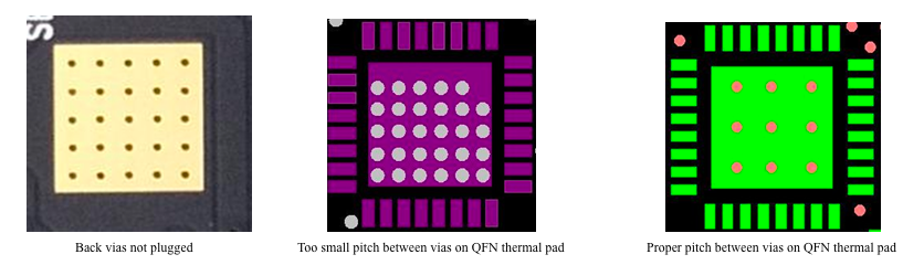
-
Do not arrange any vias within the windows painted with green ink on both faces or within the layout of the component pads. Except the thermal vias, all vias less than 0.3 mm in diameter must be covered with green ink.
Test points
-
Arrange at least one test point in each trace. Try to distribute all test points at the bottom to facilitate the creation of the test fixture.
-
The radio frequency connector test pad is 4.5 mm or more away from the edge of the test point that includes TX, RX, and PWM.
-
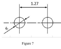
The center distance between two adjacent test points is at least 1.27 mm and recommended to be 2.54 mm or more, as shown in Figure 7.
-
The diameter of each test point ranges from 0.8 mm to 1.0 mm.
-
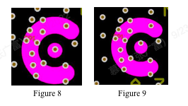
In principle, do not place vias at test points. If any, try to place them close to the edge of a test point. Do not place any vias at the center of a test point. This avoids poor contact between the pins and test points during testing. Figure 8 shows the improper placement and Figure 9 shows the qualified one.
-
Do not design other irrelevant components between test points. The distance between a test point and a component pad is 1 mm or more. This avoids short circuits between components or test points. Test points cannot be covered with any insulation layers.
Design of components processed with wave soldering
-
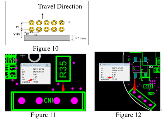
The pitch P1 or P2 between the centers of wave soldering pads for through-hole components must be more than 0.65 mm and is recommended to be more than 1 mm, as shown in Figure 10.
-
The distance between the SMT component body on the front wave soldering surface or the wave soldering component body and the board edge must be more than 1 mm and is recommended to be more than 2 mm, as shown in Figure 11.
-
The distance between the wave soldering pad for a through-hole component and the board edge must be 1.5 mm or more, and is recommended to be 3 mm or more.
-
For wave soldering that applies clamps, the distance between the through-hole component pad and the edge of the SMT pad or component body must be 1.5 mm or more and is recommended to be 3 mm or more, as shown in Figure 12. Bottom SMT components must be within 4 mm in height. Bottom components can be up to 8 mm in height.
-
For the wave soldering process that applies red glue, the pitch between pad edges must be more than 0.65 mm and is recommended to be more than 1 mm. The distance from SMT components at panel hollows to the board edge must be more than 2 mm and is recommended to be more than 3 mm.
-
Do place any surface-mounted device (SMD) within a distance of 3 mm around the components that will be frequently plugged in or out.
-
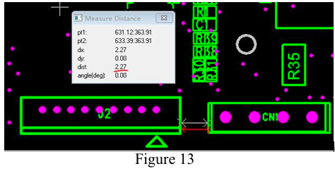
The pitch between silkscreens on through-hole components must be more than 0.5 mm, as shown in Figure 13.
Dimensions of through holes
-
If the material pin is in a circle shape:
- Diameter of PCB through hole = Diameter of actual pin + 0.20 mm to 0.30 mm (8.0 mils to 12 mils).
- Recommended: Diameter of PCB through hole = Diameter of actual pin + 0.30 mm (12 mils).
-
If the material pin is in a square shape:
Diameter of PCB through hole = Diameter of actual pin diagonal + 0.10 mm to 0.20 mm (4.0 mils to 8 mils).
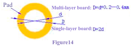
Dimensions of pads
Recommended dimensions of regular pads = Diameter of through hole + 0.50 mm (20 mils), as shown in Figure 14.
Specifications of pads
-
The length of a single edge for all pads must be at least 0.25 mm. The diameter of a pad must be at most three times the diameter of the component through hole. In most cases, through-hole components apply circular pads. The pad diameter must be over 1.8 times the diameter of a through hole. The diameter of a single-surface SMT pad must be at least 2 mm. For a dual-surface SMT pad, the ratio of the pad diameter and the through-hole diameter is recommended to be 2.5. For automatic through-hole components: Diameter of dual-surface SMT pad = Standard pad diameter + 0.5 mm to 0.6 mm.
-
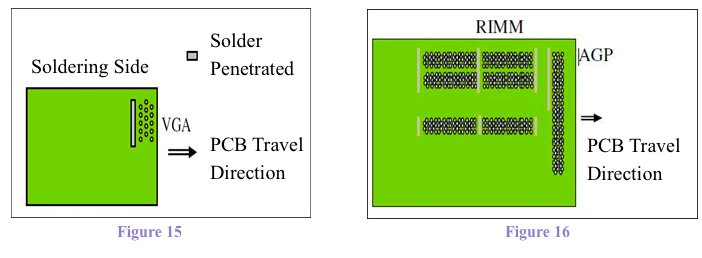
Try to keep a distance of over 0.5 mm between the edges of two pads. For the array of pads perpendicular to the wave soldering production direction, the pitch between pads must be at least 0.65 mm. If the pitch is too small, bridging might be incurred. If the distance between pad edges is less than 0.5 mm, apply white oil to reduce bridging during wave soldering. For pads in an ellipse or long circle shape, keep a small pitch between pins or connectors. For the last array of pins on the PCB, solder can penetrate the pad along the PCB travel direction to improve tinning during wave soldering, as shown in Figures 15 and 16.
Suggestions on stencil openings
Dimensions
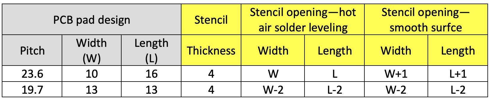
The dimensions of stencil openings for solder paste printing depend on the model of printing machines. Common dimensions include 29 inches × 29 inches, 23 inches × 23 inches, and 650 mm × 550 mm. The recommended dimensions are 29 inches × 29 inches.
Thickness
-
Stencil openings and opening wall thickness are critical to excellent printing quality. The aperture area ratio (AAR) is the factor that determines the applicable types of stencil openings.
-
AAR ≥ 0.66: applies to stencil openings that are cut by lead or lead-free lasers and electropolished stencils.
-
AAR ≥ 0.55: applies to lead or lead-free electroformed stencils.
-
AAR < 0.55: applies to nanocoated stencils.
-
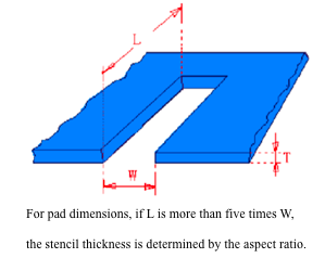
Design rules specified in IPC-7525B Stencil Design Guidelines to facilitate the effective release of solder paste: aspect ratio > 1.5, area ratio > 0.66.
-
If stencil openings do not meet the preceding AAR rules, contact Tuya’s engineers to determine whether the stencil needs to be partially thickened or thinned. Before the stencil thickness is determined, check the pitches between component pads. Certain pads are very close to each other.
-
0.005": the standard thickness of solder paste stencils
-
0.006": the standard thickness of stencils for glue printing
-
0.008": recommended when a gap exists between the printing glue and circuit board.
-
The stencil thickness depends on the area ratio and aspect ratio.
Step stencil
Consider how the area ratio works on the transfer efficiency, solder paste release, and volume repetition. Then, a partially thickened or thinned stencil might have a positive impact on the absolute volume and standard deviation of deposits. To get an optimal area ratio, use a partially thinned stencil. To get a volume larger than a theoretical stencil opening volume, use a partially thickened stencil.
To make electroformed stencils thinned by 1 mil in a stepped manner, leave a pitch of at least 30 mils between the partially thickened or thinned positions and stencil openings.
Stencil alignment
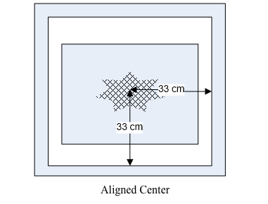
Pointing the center of openings at the stencil is a standard step in stencil printing.
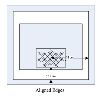
The board edges are aligned with stencil edges. The figure above shows the reference for the distances between the board edges and stencil edges in the x- and y-coordinate directions.
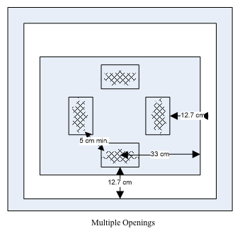
- For multiple openings, a distance of at least 5 cm is kept between PCBs.
- The board edges are aligned with stencil edges. In the x- and y-coordinate directions, the distance between the board edges and stencil edges must be at least 12.7 cm.
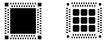
QFN stencil openings for dual-row pads
-
The coverage rate of openings on a thermal pad is about 40% to 60%.
-
The coverage rate of openings on a square pad is about 50%.
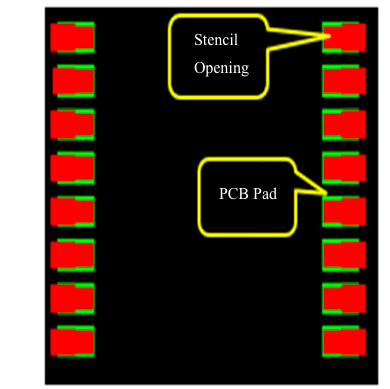
Stencil openings on motherboard pads
-
The thickness of the stencil on a development board PCBA motherboard ranges from 0.12 mm to 0.15 mm. If the stencil thickness is less than 0.12 mm due to the 0201 package or other components that are arranged at a small pitch, use a step stencil that is partially thickened. This ensures sufficient tinning on the pad.
-
The stencil openings are separately optimized on the development board PCBA motherboard. Along the width direction of the pad, the upper and lower edges are shrunk inward to avoid solder beads. The pad is shrunk inward and moved outward along the length direction to increase tinning.
-
Along the width direction of the pad, the upper and lower edges are shrunk inward by 10%, that is the module’s lead length, to avoid solder beads.
-
Along the direction of length, the stencil openings are shrunk inward by 10% to 20%, and moved outward by 20% to 40%.
-
Use a step stencil to increase tinning if necessary.
Suggestions on solder paste printing
-
Solder paste must be strictly managed and controlled as required by the solder paste manufacturer. Before solder paste printing, make sure the solder paste is within its shelf life and has been warmed up and stirred. For more information about the warm-up and stirring duration, see the datasheet of solder paste. If the datasheet is unavailable, we recommend that you warm up the solder paste for 2 hours to 4 hours and stir it for 1 minute to 3 minutes if the solder paste is refrigerated at a temperature from 2°C to 10°C. We recommend that you use the solder paste within 24 hours after it is unpacked.
-
Printing parameters are subject to the characteristics of the solder paste product, and printing device. Recommended parameters: The printing speed ranges from 40 mm/s to 70 mm/s. The printing pressure ranges from 0.018 kg to 0.027 kg per unit length of the scraper in mm. For example, for a 300 mm scraper, the printing pressure ranges from 5.4 kg to 8.1 kg. During printing, the working area of the scraper must have little residual solder paste.
-
Check the solder printing quality. Without a solder paste inspection (SPI) machine, you must arrange for staff to visually inspect the offset, thickness, area, and volume of the solder paste printing. Recommended SPI inspection parameters: Based on the actual stencil openings, the parameters are set for the partially-thickened area separately from that with normal thickness.
- Offset: ± 30%
- Thickness: 60% to 170%
- Area: 60% to 170%
- Volume: 50% to 180%These parameters are provided for your reference. An SPI device is an optical inspection device. Certain deviations might exist during the inspection. The inspection parameters can be optimized to suit your actual conditions. This helps to locate printing defects prior to the SMT process. Excessive false positive is not recommended.
Suggestions on SMT application
-
Before feeding, check all moisture-sensitive components to determine whether the 10% relative humidity indicator turns pink in the vacuum package. If so, bake the devices as specified in the management and control specifications for moisture-sensitive components.
-
Make sure the components are absorbed and mounted with the expected precision. For this purpose, package all materials with a tape and reel option or a standard SMT tray and meet SMT requirements.
-
Select a suction nozzle in a size suitable for suction and SMT application. The area of the suction nozzle is recommended to be 40% to 60% of the area of the sucked material. Set the speed to low.
-
During image recognition, try to use the pad or component pin for positioning to ensure stable image recognition. Control the SMT precision to be within ±0.1 mm.
-
Mount the component in the direction strictly along the external frame of the silk screen. The recommended packaging defines the dimensions and direction of the external frame of the silk screen.
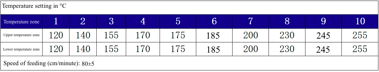
Suggestions on reflow soldering
If SAC305 lead-free solder paste is used, set the oven temperature as described in the following table. You can adjust the temperature values according to the actual reflow soldering device, PCB thickness, and component structure. The oven temperature for all components must fall within the process limits.
Oven temperature curve
Use an actual board to create a temperature test board. We recommend that you test the oven temperature each time the product is replaced. During continuous production, test the oven temperature curve once per day. Set the oven temperature curve as recommended in the following process limits.
SMT oven temperature curve
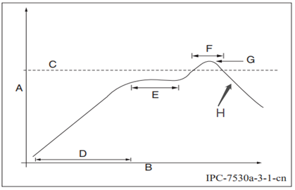
-
A: temperature axis
-
B: time axis
-
C: alloy liquidus temperature from 217°C to 220°C
-
D: ramp-up slope from 1°C/s to 3°C/s
-
E: constant temperature time from 60s to 120s, constant temperature from 150°C to 200°C
-
F: temperature above liquidus temperature for 50s to 70s
-
G: peak temperature from 235°C to 245°C
-
H: ramp-down slope from 2°C/s to 4°C/s
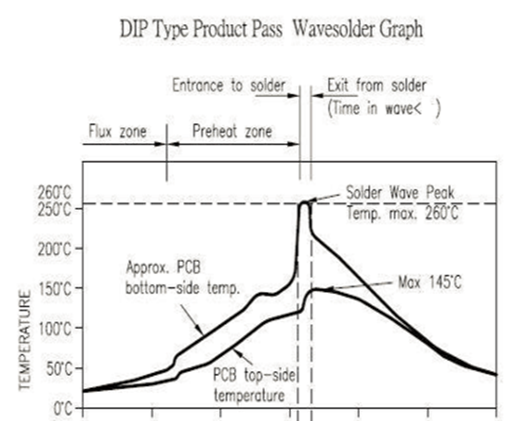
DIP oven temperature curve
Use SAC305 lead-free solder bars. You can adjust the temperature values according to the actual reflow soldering device, PCB thickness, and component structure. The oven temperature for all components must fall within the process limits.
-
A: preheating temperature from 80°C to 130°C
-
B: preheating duration from 75s to 100s
-
C: contact duration at the peak from 3s to 5s
-
D: solder tank temperature at 260±5°C
-
E: ramp-up slope ≤ 2°C/s
-
F: ramp-down slope ≤ 6°C/s
Wave soldering fixture
To design a wave soldering fixture, first create openings as identified by location numbers of through-hole materials listed in the bill of materials (BOM). The soldering quality of all through-hole components conforms with the appearance requirements specified in IPC-A-610 Class 2. Add slates or limit bars to special components to get the qualified appearance of through-hole components and prevent floating or skewed components. The following sections describe how to create a wave soldering fixture for sockets of Australian standards. These steps are for your reference.
-
Add a clam to the wave soldering fixture to hold and fix the module board and make the module board soldered perpendicularly to the PCB.
-
Fix FR-4 limit bars on the fixture and insert and fix the module board into a slot of the fixture.
-
Put a bakelite magnetic slate on the fixture to cover the module, and point the module board at the slot.
Process control standards on manual soldering
-
To create a manual soldering fixture, first create openings as identified by location numbers of manual soldering materials listed in the bill of materials (BOM). Fasten the PCBA stably on the manual soldering fixture and protect soldered material components from floating to achieve the expected soldering result.
-
If SAC305 lead-free solder paste is used, set the soldering temperature to 370°C±10°C.

-
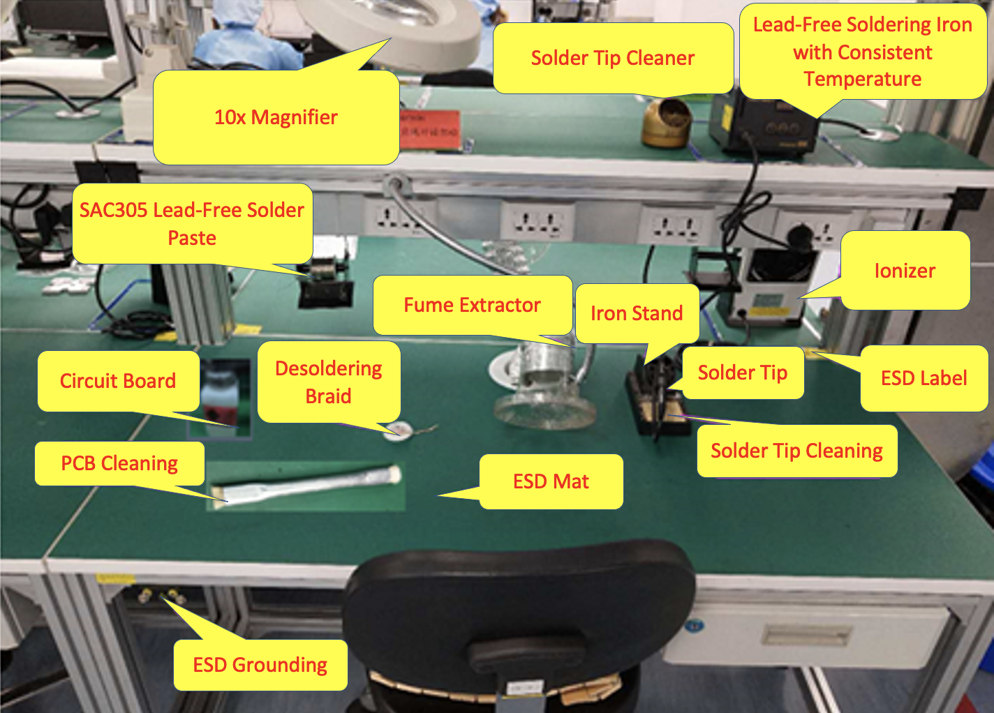
The following figure shows the layout of the manual soldering station.
-
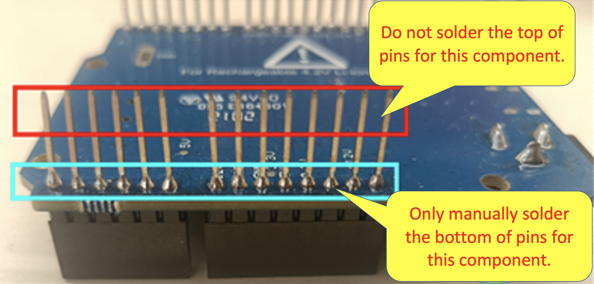
The following figure shows the requirements on manual soldering of special components for development boards.
Development board PCBA flowchart
SMT flowchart
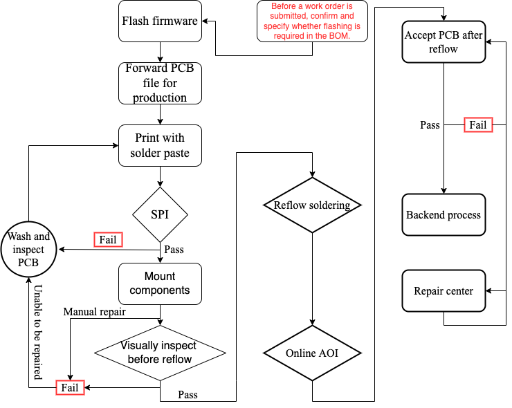
For QFN, land grid array (LGA), and ball grid array (BGA) components, use x-ray to inspect the soldering quality. Specifically, detect solder bridges and insufficient wetting and check whether the solder void ratio is 30% or lower.
DIP flowchart
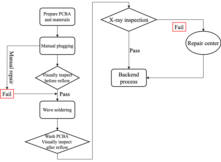
For through-hole components, use x-ray to check whether the solder filling height is 75% or higher and whether the solder void ratio is 30% or lower.
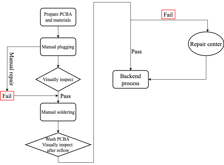
Manual soldering flowchart
For through-hole components, use x-ray to check whether the solder filling height is 75% or higher and whether the solder void ratio is 30% or lower.
Is this page helpful?
YesFeedbackIs this page helpful?
YesFeedback


