Wi-Fi Module TYJW2S-5V
Product Overview
After a period of service, this module will become deprecated due to product upgrades and iterations, user requirements, production inventory, or other reasons. To improve the compatibility of your smart devices and minimize the impact on your use, Tuya continues to provide webpage documentation of deprecated modules, but no longer maintains or updates the documentation. The content herein is for reference only.
If you have any questions, submit a ticket to contact Tuya or consult Tuya’s account manager to request support. If you need similar substitute products, see JWBR2S-5V or WBR Module Datasheet.
TYJW2S-5V is a Wi-Fi module with a 5V TTL UART series port interface designed by Hangzhou Tuya Information Technology Co., Ltd. The module consists of a Tuya Wi-Fi module and some power-level converter circuits, which have been programmed with Wi-Fi network protocol and plenty of software examples.
TYJW2S-5V is an RTOS platform, embedded with all the Wi-Fi MAC and TCP/IP protocol function examples, users can customize their Wi-Fi product by using these software examples.
Figure 1 shows the block diagram of the TYJW2S-5V:
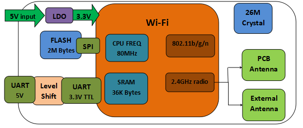
Figure 1 The block diagram of the TYJW2S-5V
Feature
-
Integrated low power consumption 32-bit CPU, also known as application processor
Basic frequency can support 80MHz and 160MHz -
Supply voltage range: TYJW2S-5V support 4.5V ~ 5.5V
-
Peripherals: 1*UART (TTL)
-
Wi-Fi connectivity:
-
802.11 b/g/n
-
Channel 1-14@2.4GHz
-
Support WPA/WPA2
-
+20dBm output power in 802.11b mode
-
Support STA/AP/STA+AP operation mode
-
Support SmartConfig function for both Android and IOS devices
-
-
On-board PCB antenna or IPEX connect for external antenna
-
Operating temperature range: -20℃ to 85℃
Main Application Fields
- Intelligent Building
- Intelligent home, Intelligent household applications
- Health care
- Industrial wireless control
- Portable devices
Dimensions and Footprint
Dimensions
TYJW2S-5V has an interface of PH-4AW connection port. The distance between each Pin is 2mm. The interface is a PH2.04-Y connector.
Size of TYJW2S-5V: 42.6mm(W)*31mm(L)*9.1mm(H)
Figure 2 shows the dimensions of TYJW2S-5V.
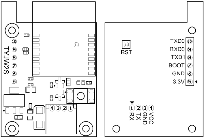
Front view Back view
Pin Definition
Table 1 shows the general pin attributes of TYJW2S-5V
Table 1 The typical pin definition of TYJW2S-5V
| PIN NO. | NAME | TYPE | DESCRIPTION |
|---|---|---|---|
| 1 | RX | I/O | RX port, input 5V TTL |
| 2 | TX | I/O | TX port, output 5V TTL |
| 3 | GND | P | Ground |
| 4 | VCC | P | Supply Voltage 5V |
Note: S: Power supply pins; I/O: Digital input or output pins;
Test Point Definition
The test point pin definition is shown in Table 2:
Table 2 The typical pin definition of TYJW2S-5V
| PIN NO. | NAME | TYPE | DESCRIPTION |
|---|---|---|---|
| 5 | 3.3V | P | Internal 3.3V voltage pin |
| 6 | GND | P | Ground |
| 7 | BOOT | I/O | IO0 pin, firmware burning selection pin |
| 8 | TXD1 | I/O | Information print pin |
| 9 | RXD0 | I/O | Firmware burning pin |
| 10 | TXD0 | I/O | Firmware burning pin |
| 11 | RST | I/O | Reset pin |
Note: P: Power supply pins; I/O: Digital input or output pins
If IO0 is unconnected, the module is in normal working mode; If IO0 is in a negative level, the module is in firmware burning mode.
RST is used for module hardware reset, and cannot clear Wi-Fi connection information.
This test point is not recommended for regular usage.
Electrical Characteristics
Absolute Maximum Ratings
Table 3 Absolute Maximum Ratings
| PARAMETERS | DESCRIPTION | MIN | MAX | UNIT |
|---|---|---|---|---|
| Ts | Storage temperature | -20 | 85 | ℃ |
| VCC (TYJW2S-5V) | Supply voltage | -0.3 | 5.5 | V |
| VCC (TYJW2S-3.3V) | Supply voltage | -0.3 | 3.6 | V |
| Static electricity voltage (human model) | TAMB-25℃ | - | 2 | KV |
| Static electricity voltage (machine model) | TAMB-25℃ | - | 0.5 | KV |
Electrical Conditions
Table 4 Electrical Conditions
| PARAMETERS | DESCRIPTION | MIN | TYPICAL | MAX | UNIT |
|---|---|---|---|---|---|
| Ta | Working temperature | -20 | - | 85 | ℃ |
| VCC (TYJW2S-5V) | Working voltage | 4.5 | 5 | 5.5 | V |
| VCC(TYJW2S-3.3V) | Working voltage | 3.0 | 3.3 | 3.6 | V |
| VIL | IO negative level input | -0.3 | - | VCC*0.25 | V |
| VIH | IO positive level input | VCC*0.75 | - | VCC | V |
| VOL | IO negative level output | - | - | VCC*0.1 | V |
| VoH | IO positive level output | VCC*0.8 | - | VCC | V |
| Imax | IO drive current | - | - | 5 | mA |
Wi-Fi Transmitting Current Consumptions
Table 5 Wi-Fi TX current consumption
| PARAMETERS | MODE | RATE | TYPICAL | UNIT |
|---|---|---|---|---|
| IRF | 11b | 11Mbps | 260 | mA |
| IRF | 11g | 54Mbps | 100 | mA |
| IRF | 11n | MCS7 | 100 | mA |
Wi-Fi Receiving Current Consumptions
Table 6 Wi-Fi RX current consumption
| PARAMETERS | MODE | RATE | TYPICAL | UNIT |
|---|---|---|---|---|
| IRF | 11b | 11Mbps | 70 | mA |
| IRF | 11g | 54Mbps | 70 | mA |
| IRF | 11n | MCS7 | 70 | mA |
Working Mode Current Consumptions
Table 7 MCU working current consumption
| WORK MODE | AT TA=25℃ | TYPICAL | MAX* | UNIT |
|---|---|---|---|---|
| EZ Mode | Module is under EZ paring mode, Wi-Fi indicator light flashes quickly | 90 | 436 | mA |
| AP Mode | Module is under AP paring mode, Wi-Fi indicator light flashes slowly | 101 | 451 | mA |
| Operation Mode | Module is connected, Wi-Fi indicator light is on | 58.5 | 411 | mA |
| Disconnection Mode | Modules is disconnected, Wi-Fi indicator light is off | 156 | 430 | mA |
WLAN Radio Specification
Basic Radio Frequency Characteristics
Table 8 Basic radio frequency characteristic
| PARAMETERS | DESCRIPTION |
|---|---|
| Frequency band | 2.400GHz to 2.4835GHz |
| Wi-Fi standard | IEEE 802.11n/g/b (Terminal 1-14) |
| Data transmitting rate | 11b: 1, 2, 5.5, 11(Mbps) 11g: 6, 9, 12, 18, 24, 36, 48, 54(Mbps) 11n: HT20, MCS0~7 |
| Antenna type | On-board PCB Antenna (Default), UF.L RF external antenna (optional) |
Wi-Fi Transmitting Power
Table 9 Wi-Fi transmitting power
| PARAMETERS | MIN | TYPICAL | MAX | UNIT | |
|---|---|---|---|---|---|
| RF average output power, 802.11b CCK Mode | 1M | - | 17 | - | dBm |
| RF average output power, 802.11g OFDM Mode | 54M | - | 15 | - | dBm |
| RF average output power, 802.11n OFDM Mode | MCS7 | - | 13 | - | dBm |
| The Frequency error | -10 | - | 10 | ppm |
Wi-Fi Receiving Sensitivity
Table 10 Wi-Fi Receiving sensitivity
| PARAMETERS | MIN | TYPICAL | MAX | UNIT | |
|---|---|---|---|---|---|
| PER<8%, Receiving sensitivity, 802.11b CCK Mode | 1M | - | -91 | - | dBm |
| PER<10%, Receiving sensitivity, 802.11g OFDM Mode | 54M | - | -75 | - | dBm |
| PER<10%, Receiving sensitivity, 802.11n OFDM Mode | MCS7 | - | -72 | - | dBm |
Antenna Information
Antenna Type
The antenna can be connected using an on-board PCB antenna or an external antenna; the default way is using the on-board PCB antenna. If an external antenna is needed, please contact the BD manager.
Reduce Antenna Interference
While using the on-board PCB antenna, in order to have the best Wi-Fi performance, it’s recommended to keep a minimum 15mm distance between the antenna part and the other metal pieces.
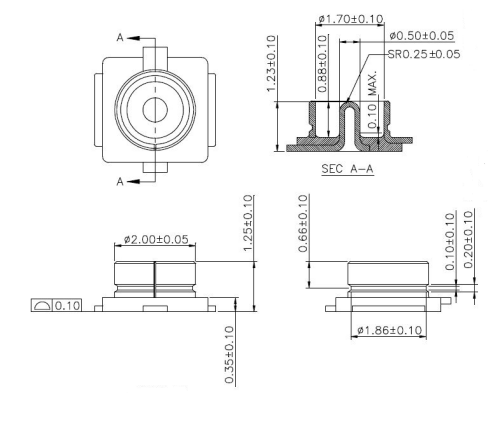
U.FL RF Connector
Figure 3 shows the physical parameter of the U.FL RF connector.
Packaging Information And Production Guide
Mechanical Dimensions
Figure 4 Top view of the module
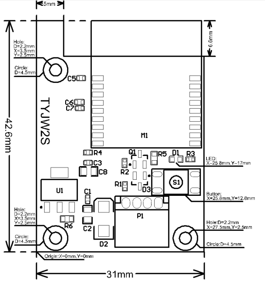
Note: the tolerance of the PCB outline border is ±0.15mm, and the tolerance of PCB thickness is ±0.1mm
Production Guide
The storage for the delivered module should meet the following condition:
- The anti-moisture bag should be kept in an environment with a temperature < 30℃ and humidity < 85% RH.
- The expiration date is 6 months since the dry packaging products were sealed.
Cautions:
- All the operators should wear an electrostatic ring in the whole process of production.
- While operating, water and dirt should not contact the modules.
Wire parameter
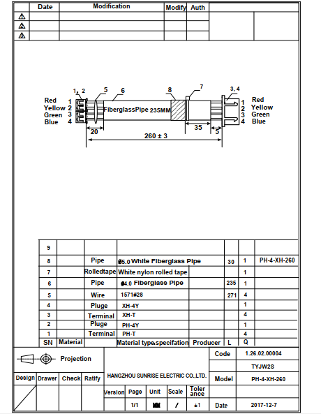
Figure 5 Wiring specification parameters
Shell parameter
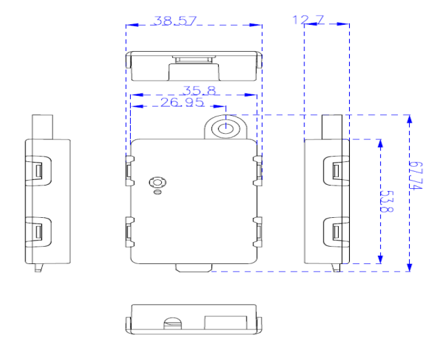
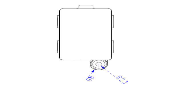
Figure 6 Shell parameters
Is this page helpful?
YesFeedbackIs this page helpful?
YesFeedback


