JWBR2S-5V Module Datasheet
Product overview
Developed by Tuya, JWBR2S-5V is a Wi-Fi module suitable for serial communication of the 5V TTL. It consists of a WBR1 module, which supports both the Wi-Fi and Bluetooth communication protocols and a level conversion circuit. It is further embedded with the Wi-Fi/Bluetooth network protocol stack and Tuya serial communication protocol.
JWBR2S-5V is an RTOS platform. On the basis of the serial communication manner, you can develop embedded products as required.
Features
- Embedded low-power KM4-MCU, which can also function as an application processor
- The maximum clock rate: 100 MHz
- Operating voltage: 5V
- Peripheral: 1 UART
- Wi-Fi connectivity
- 802.11 b/g/n20/
- Channels 1 to 14@2.4 GHz
- Support Bluetooth Low Energy 4.2
- Support WPA/WPA2 security mode
- Up to +18dBm output power in 802.11b mode
- Support SmartConfig for Android and iOS devices
- Onboard PCB antenna
- Operating temperature: -20℃ to 85℃
Applications
- Intelligent building
- Smart household and home appliances
- Smart socket and light
- Industrial wireless control
- Baby monitor
- Network camera
- Intelligent bus
Module interfaces
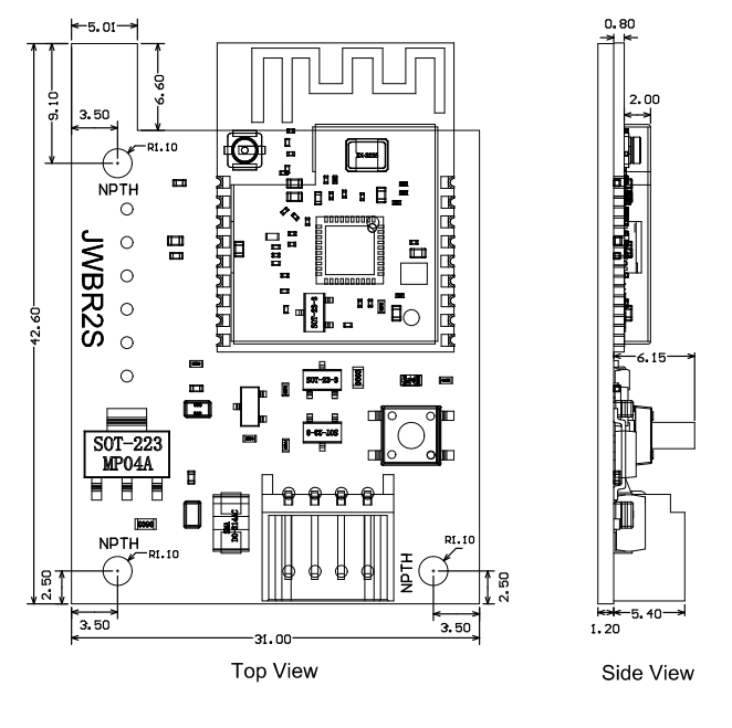
Dimensions and footprint
The electrical interface of JWBR2S-5V is the PH-4AW connector with a spacing of 2.0 mm.
As shown in the following figure, the dimensions of JWBR2S-5V are 42.6±0.35 mm (W) × 31±0.35 mm (L) × 9.1±0.15 mm (H). The thickness of the PCB is 1.2±0.1 mm.
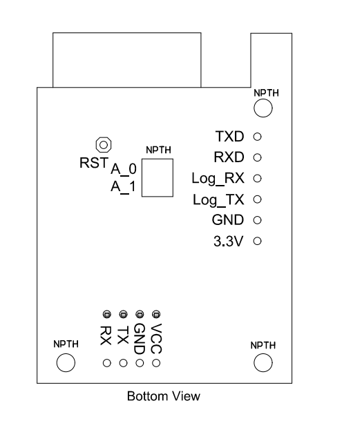
Pin definition
| Pin number | Symbol | Type | Function |
|---|---|---|---|
| 1 | RX | I/O | UART0_RXD, receiving interface the module, input the level of 5V TTL |
| 2 | TX | I/O | UART0_TXD, transmitting interface of the module, output the level of 5V TTL |
| 3 | GND | P | Power supply reference ground |
| 4 | VCC | P | Power supply pin (5V) |
Note:
Pindicates power supply pins andI/Oindicates input/output pins.
Definitions on test pins
| Pin number | Symbol | Type | Function |
|---|---|---|---|
| 1 | 3.3V | P | Power supply pin inside the module (3.3V) |
| 2 | GND | P | Power supply reference ground |
| 3 | Log_Tx | I/O | UART_Log_TXD (used to display the internal information of the module) |
| 4 | Log_Rx | I/O | UART_Log_RXD (used to display the internal information of the module) |
| 5 | RXD | I/O | Interface for programming firmware of the module |
| 6 | TXD | I/O | Interface for programming firmware of the module |
| 7 | A_0 | I/O | GPIOA_0, interface for programming firmware of the module When powered on, the pin needs to be pulled to 3.3V. |
| 8 | RST | I/O | Hardware reset pin |
Note:
Pindicates power supply pins,I/Oindicates input/output pins and test points are prohibited.
Electrical parameters
Absolute electrical parameters
| Parameter | Description | Minimum value | Maximum value | Unit |
|---|---|---|---|---|
| Ts | Storage temperature | -40 | 105 | ℃ |
| VBAT | Supply voltage | -0.3 | 5.5 | V |
| ESD voltage (human body model) | TAMB-25℃ | - | 2 | KV |
| ESD voltage (machine model) | TAMB-25℃ | - | 0.5 | KV |
Normal working conditions
| Parameter | Description | Minimum value | Typical value | Maximum value | Unit |
|---|---|---|---|---|---|
| Ta | Working temperature | -20 | - | 85 | ℃ |
| VBAT | Supply voltage | 4.5 | 5 | 5.5 | V |
| VIL | Voltage Input Low | -0.3 | - | 0.825 | V |
| VIH | Voltage Input High | 2.475 | - | 3.3 | V |
| VOL | Voltage Output Low | - | - | 0.33 | V |
| VOH | Voltage Output High | 2.64 | - | 3.3 | V |
| Imax | Drive current | - | - | 16 | mA |
| Cpad | Input pin capacitance | - | 2 | - | pF |
TX power consumption
| Working status | Mode | Rate | Transmit power | Average value | Peak value (typical value) | Unit |
|---|---|---|---|---|---|---|
| Transmit | 11b | 11Mbps | +17.5dBm | 269.1 | 299.9 | mA |
| Transmit | 11g | 54Mbps | +14.5dBm | 166.8 | 233.1 | mA |
| Transmit | 11n BW20 | MCS7 | +13.5dBm | 164.2 | 226.5 | mA |
RX power consumption
| Working status | Mode | Receive | Average value | Peak value (typical value) | Unit |
|---|---|---|---|---|---|
| Receive | CPU Active | 11Mbps | 65.7 | 73.7 | mA |
| Receive | CPU Active | 54Mbps | 65.2 | 73 | mA |
| Receive | CPU Active | MCS7 | 66.2 | 73.8 | mA |
Power consumption in working mode
| Working mode | Working status, Ta = 25°C | Average value | Peak value (typical value) | Unit |
|---|---|---|---|---|
| EZ | The module is in fast connection state | 60 | 291.5 | mA |
| Idle state of network connection | The module is in idle state of network connection | 60.3 | 239.5 | mA |
| Operation state of network connection | The module is connecting to the network | 60.2 | 287.5 | mA |
| Disconnected state | The module is disconnected | 61 | 288 | mA |
Note: The peak lasts about 5μs. The above parameters may vary with different firmware functions.
RF parameters
Basic RF features
| Parameter | Description |
|---|---|
| Working frequency | 2.400 to 2.484 GHz |
| Wi-Fi standard | IEEE 802.11 b/g/n (channels 1 to 14) |
| Data transmission rate | 11b: 1, 2, 5.5, and 11 (Mbps); 11g: 6, 9, 12, 18, 24, 36, 48, and 54 (Mbps); 11n: HT20 MCS 0 to 7 |
| Antenna type | PCB antenna |
TX performance
TX performance
| Parameter | Minimum value | Typical value | Maximum value | Unit |
|---|---|---|---|---|
| Average output power, 802.11b CCK Mode 11M | - | 17.5 | - | dBm |
| Average output power, 802.11g OFDM Mode 54M | - | 14.5 | - | dBm |
| Average output power, 802.11n OFDM Mode MCS7 | - | 13.5 | - | dBm |
| Frequency error | -20 | - | 20 | ppm |
RX performance
RX sensitivity
| Parameter | Minimum value | Typical value | Maximum value | Unit |
|---|---|---|---|---|
| PER<8%, RX sensitivity, 802.11b DSSS Mode 1M | - | -91 | - | dBm |
| PER<10%, RX sensitivity, 802.11g OFDM Mode 54M | - | -75 | - | dBm |
| PER<10%, RX sensitivity, 802.11n OFDM Mode MCS7 | - | -72 | - | dBm |
Antenna information
Antenna type
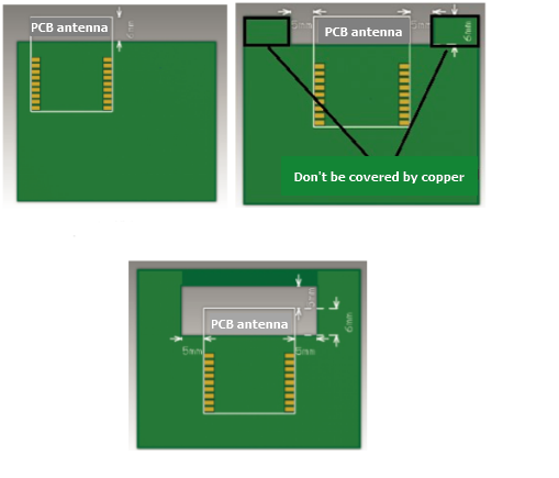
JWBR2S-5V supports two types of antennas: Onboard PCB antenna and external antenna. By default, the onboard PCB antenna is preferred.
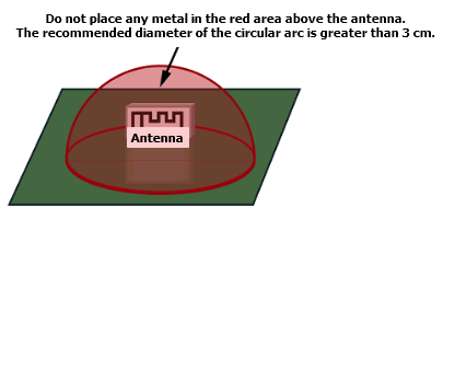
Antenna interference reduction
To ensure optimal Wi-Fi performance when the Wi-Fi module uses an onboard PCB antenna, it is recommended that the antenna be at least 15 mm away from other metal parts.
To prevent adverse impact on the antenna radiation performance, avoid copper or traces within the antenna area of the PCB.
Specifications of antenna connector
There is no antenna connector for this module currently.
Power-on sequence
The chip has requirements on the power-on sequence. It is recommended that the voltage should rise from 0 to 3.3V within 40mS.
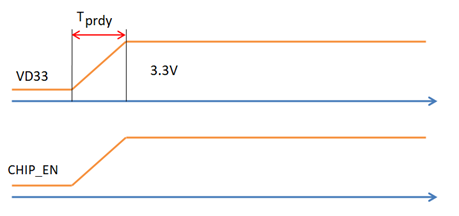
| Symbol | Parameter | Minimum value | Typical value | Maximum value | Unit |
|---|---|---|---|---|---|
| TPRDY | 3.3V ready time | 0.6 | 40 | mS | |
| CHIP_EN | CHIP_EN ready time | 0.6 | 40 | mS |
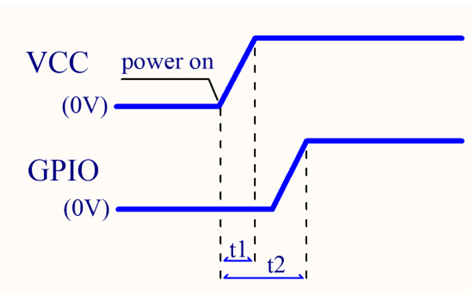
The high-level establishment time t2 for the TX and RX pins of the adapter board should be less than the high-level establishment time t1 for the power supply. Before the power supply pin of the adapter board is powered on, the MCU should not pull the level of the TX/RX pin to be high.
Packaging information and production instructions
Mechanical dimensions
As shown in the following figure, the dimensions of JWBR2S-5V are 42.6±0.35 mm (W) × 31±0.35 mm (L) × 9.1±0.15 mm (H). The thickness of the PCB is 1.2±0.1 mm.
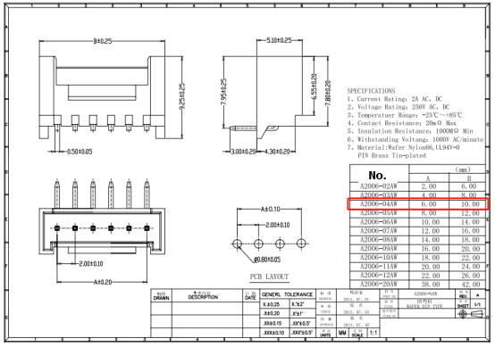
Specifications of terminal
The terminal has 4 pins with a spacing of 2.0 mm between each other. Detailed parameters are as follows:
Storage conditions
-
Temperature and humidity control: It should be stored in an environment where temperature and humidity can be controlled. The ideal storage temperature is generally between 0-35°C, with humidity kept below 60%. Excessively high temperatures and humidity may lead to oxidation or corrosion of metal parts, while excessively low temperatures may cause materials to become brittle and prone to breaking.
-
Avoid direct sunlight: Direct exposure to sunlight may cause aging or degradation of the materials.
-
Waterproof and dustproof: The storage environment should remain dry to prevent moisture ingress, as moisture can lead to internal circuit short circuits or damage. Additionally, it is important to protect the module from dust and other solid impurities, as this may affect the product’s contact performance and stability.
-
Avoid corrosive environments: The storage environment should avoid the presence of corrosive substances, as these can corrode the metal parts of the product and reduce its lifespan.
Appendix:Statement
FCC Caution: Any changes or modifications not expressly approved by the party responsible for compliance could void the user’s authority to operate this device.
This device complies with Part 15 of the FCC Rules. Operation is subject to the following two conditions: (1) This device may not cause harmful interference, and (2) this device must accept any interference received, including interference that may cause undesired operation.
Note: This device has been tested and found to comply with the limits for a Class B digital device, according to part 15 of the FCC Rules. These limits are designed to provide reasonable protection against harmful interference in a residential installation. This device generates, uses, and can radiate radio frequency energy and, if not installed and used following the instructions, may cause harmful interference to radio communications. However, there is no guarantee that interference will not occur in a particular installation.
If this device does cause harmful interference to radio or television reception, which can be determined by turning the device off and on, the user is encouraged to try to correct the interference by one or more of the following measures:
- Reorient or relocate the receiving antenna.
- Increase the separation between the device and receiver.
- Connect the device into an outlet on a circuit different from that to which the receiver is connected.
- Consult the dealer or an experienced radio/TV technician for help.
Radiation Exposure Statement
This device complies with FCC radiation exposure limits set forth for an uncontrolled rolled environment. This device should be installed and operated with a minimum distance of 20cm between the radiator and your body.
Important Note
This radio module must not be installed to co-locate and operating simultaneously with other radios in the host system except following FCC multi-transmitter product procedures. Additional testing and device authorization may be required to operate simultaneously with other radios.
The availability of some specific channels and/or operational frequency bands are country dependent and are firmware programmed at the factory to match the intended destination. The firmware setting is not accessible by the end-user.
The host product manufacturer is responsible for compliance with any other FCC rules that apply to the host not covered by the modular transmitter grant of certification. The final host product still requires Part 15 Subpart B compliance testing with the modular transmitter installed.
The end-user manual shall include all required regulatory information/warnings as shown in this manual, including "This product must be installed and operated with a minimum distance of 20 cm between the radiator and user body".
This device has got an FCC ID: 2ANDL-JWBR2S-5V. The end product must be labeled in a visible area with the following: "Contains Transmitter Module FCC ID: 2ANDL-JWBR2S-5V".
This device is intended only for OEM integrators under the following conditions:
The antenna must be installed such that 20cm is maintained between the antenna and users, and the transmitter module may not be co-located with any other transmitter or antenna.
As long as the 2 conditions above are met, further transmitter tests will not be required. However, the OEM integrator is still responsible for testing their end-product for any additional compliance requirements required with this module installed.
Declaration of Conformity European Notice

Hereby, Hangzhou Tuya Information Technology Co., Ltd declares that this module product is in compliance with essential requirements and other relevant provisions of Directive 2014/53/EU,2011/65/EU. A copy of the Declaration of conformity can be found at https://www.tuya.com.

This product must not be disposed of as normal household waste, in accordance with the EU directive for waste electrical and electronic equipment (WEEE-2012/19/EU). Instead, it should be disposed of by returning it to the point of sale, or to a municipal recycling collection point.
The device could be used with a separation distance of 20cm to the human body.
Is this page helpful?
YesFeedbackIs this page helpful?
YesFeedback


