HPWSMS1 Module Datasheet
HPWSMS1 is a low-power embedded Wi-Fi+Bluetooth module that Tuya has developed. It consists of a highly integrated RF chip RS9116 and a few peripherals. The single bands QMS and WMS SoCs support the full multi-protocol wireless connection. Redpine offers the Linux and Android systems the drive programs.
Features
- Wi-Fi standards
- Support the IEEE802.11 b/g/n mode
- Support the band width of 20 MHz
- Maximum transmit power: 16 dB
- Receive power: -95 dB@1M
- Frequency range: 2412 MHz to 2484 MHz
- Bluetooth standards
- Bluetooth 4.2 and Bluetooth 5.0
- Maximum transmit power: -1.5 dB (the bluetooth is only used for searching for the SSID of a device)
Working conditions
- Working voltage: 1.76 to 3.65V
- Working temperature: -40℃ to -85℃
Security features
- Hardware device identification and secret key are stored at the PUF
- Accelerators: AES 128/256, SHA 256/384/512, HMAC, RSA, ECC, ECDH, RNG, and CRC
- WPA/WPA2-Personal, WPA/WPA2 Enterprise for Client, EAP-TLS, EAP-FAST, EAP-TTLS, EAP-LEAP, and PEAP-MSCHAP-v2
- Real random
- Secure boot
- Secure and backup firmware upgrade
- FIPS140-2 compatible
Applications
- Multimedia
- Consumer electronics
- Home appliances
- Industrial and home automation
- Intelligent gateway and metering
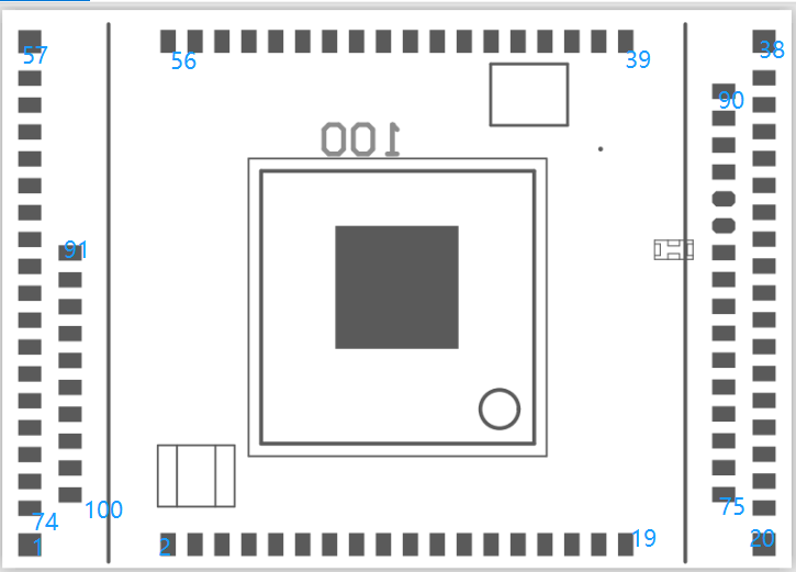
Module interfaces
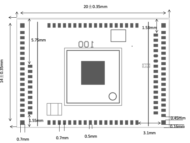
Dimensions and package
HPWSMS1 has 100 pins with a 0.7±0.1 mm pin spacing.
The HPWSMS1 dimensions are 20±0.35 mm (W) ×14±0.35 mm (L) ×3±0.15 mm (H).
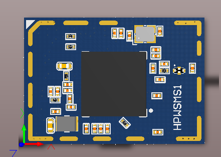
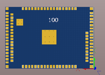
HPWSMS1 is shown below:
Pin definition
| Pin No. | IC | I/O |
|---|---|---|
| 1 | GND | GND |
| 2 | NC | / |
| 3 | NC | / |
| 4 | NC | / |
| 5 | NC | / |
| 6 | NC | / |
| 7 | A35 | GPIO |
| 8 | NC | / |
| 9 | GND | GND |
| 10 | GND | GND |
| 11 | A37 | USB_ID |
| 12 | A40 | USB_DM |
| 13 | B36 | USB_DP |
| 14 | A39 | USB_AVDD_3P3, USB 3V3 power supply pin |
| 15 | B35 | USB_AVDD_1P1, USB 1V1 power supply pin |
| 16 | A38 | USB_VBUS, USB 5V power supply pin |
| 17 | VOUTLDOSOC Output of SoC LDO | Electric power conversion pin of chip |
| 18 | NC | / |
| 19 | NC | / |
| 20 | GND | GND |
| 21 | NC | / |
| 22 | A42 | SDIO_DATA3, SDIO data pin |
| 23 | A43 | SDIO_DATA2, SDIO data pin |
| 24 | B40 | SDIO_CLK |
| 25 | A1 | SDIO_CMD |
| 26 | NC | / |
| 27 | NC | / |
| 28 | NC | / |
| 29 | PA_AVDD | 3.3V power supply pin |
| 30 | GND | GND |
| 31 | GND | GND |
| 32 | RF OUT | RF output pin, connected to the antenna link at the baseboard |
| 33 | GND | GND |
| 34 | GND | GND |
| 35 | GND | GND |
| 36 | GND | GND |
| 37 | NC | / |
| 38 | GND | GND |
| 39 | B10 | HOST_BB_EN, sleep control pin, which is used for sending instructions to the host processor. When the chip enters the ULP sleep mode and gives an instruction, it is in the low logic, and when the chip exits from the ULP sleep mode and gives an instruction, it is in the high logic. |
| 40 | NC | / |
| 41 | NC | / |
| 42 | GND | GND |
| 43 | GND | GND |
| 44 | GND | GND |
| 45 | GND | GND |
| 46 | NC | / |
| 47 | GND | GND |
| 48 | GND | GND |
| 49 | VIN_MOD | 3.3V power supply pin |
| 50 | A16 | TMS, JTAG software debugging pin |
| 51 | B15 | TD0, JTAG software debugging pin |
| 52 | A17 | TCK, JTAG software debugging pin |
| 53 | B16 | TDI, JTAG software debugging pin |
| 54 | A19 | GPIO |
| 55 | NC | / |
| 56 | NC | / |
| 57 | GND | GND |
| 58 | A20 | UART1_RX |
| 59 | A21 | UART1_TX |
| 60 | B18 | GPIO |
| 61 | A22 | GPIO |
| 62 | B21 | GPIO |
| 63 | A24 | GPIO |
| 64 | B22 | GPIO |
| 65 | A27 | POC_IN, Power On Control Input |
| 66 | B24 | ULP low-power sleep control pin |
| 67 | GND | GND |
| 68 | GND | GND |
| 69 | A29 | 32.768-K crystal input pin, NC by default |
| 70 | GND | GND |
| 71 | NC | / |
| 72 | A31 | RESET_N, resetting pin Pull the voltage to 3.3V through the master MCU or pull the voltage to 3.3V by connecting to the external. |
| 73 | NC | / |
| 74 | NC | / |
| 75 | A41 | GPIO |
| 76 | B39 | SDIO_DATA0, SDIO data pin |
| 77 | A44 | SDIO_DATA1, SDIO data pin |
| 78 | SDIO_IO_VDD | 3.3V power supply pin |
| 79 | NC | / |
| 80 | NC | / |
| 81 | A4 | GPIO |
| 82 | PA_AVDD | 3.3V power supply pin |
| 83 | GND | GND |
| 84 | GND | GND |
| 85 | GND | GND |
| 86 | GND | GND |
| 87 | GND | GND |
| 88 | GND | GND |
| 89 | NC | / |
| 90 | GND | GND |
| 91 | A25 | GPIO |
| 92 | B25 | POC_OUT, Power On Control Output. |
| 93 | GND | GND |
| 94 | UULP_VBAT | 3.3V power supply pin |
| 95 | GND | GND |
| 96 | B26 | 32.768-K crystal input pin, NC by default |
| 97 | GND | GND |
| 98 | VINBCKDC | 3.3V power supply pin |
| 99 | NC | / |
| 100 | NC | / |
Electrical parameters
Absolute electrical parameters
| Parameter | Description | Minimum value | Maximum value | Unit |
|---|---|---|---|---|
| Ta | Working temperature | -40 | 85 | ℃ |
| VBAT | Power supply voltage | -0.3 | 3.9 | V |
| Static electricity discharge voltage (human body model) | TAMB-25℃ | - | 2 | KV |
| Static electricity discharge voltage (machine model) | TAMB-25℃ | - | 0.5 | KV |
Normal working conditions
| Parameter | Description | Minimum value | Typical value | Maximum value | Unit |
|---|---|---|---|---|---|
| Ta | Working temperature | -40 | - | 85 | ℃ |
| VCC | Working voltage | 1.76 | 3.3 | 3.65 | V |
Power consumption during constant transmission, receiving, and sleep
| Working status | Mode | Rate | Transmit power/Receive | Average value | Peak value (Typical value) | Unit |
|---|---|---|---|---|---|---|
| Transmit | 11b | 11Mbps | +17.5dBm | 288 | 455 | mA |
| Transmit | 11g | 54Mbps | +15dBm | 156 | 228 | mA |
| Transmit | 11n-HT20 | MCS7 | +15dBm | 130 | 227 | mA |
| Receive | 11b | 11Mbps | Constantly receive | 125 | 129.7 | mA |
| Receive | 11g | 54Mbps | Constantly receive | 125 | 129.7 | mA |
| Receive | 11n-HT20 | MCS7 | Constantly receive | 125 | 129.7 | mA |
| Sleep mode | / | / | the average of current within the 6 min’s test time | 120 | / | uA |
RF parameters
Basic RF features
| Parameter | Description |
|---|---|
| Working frequency | Wi-Fi: 2.412 to 2.484 Ghz (Channels 1 to 11 for US/CA); Bluetooth: 2402 to 2480 MHz |
| Wi-Fi standard | IEEE 802.11b/g/n |
| Data transmission rate | Wi-Fi: 11b: 1, 2, 5.5, 11 (Mbps); 11g: 6, 9, 12, 18, 24, 36, 48, 54 (Mbps); 11n: HT20 MCS 0 to 7; Bluetooth 1M/2M |
| Antenna type | There is a reserved antenna interface pin on the module. Actually, the antenna should be on the baseboard |
TX performance
2.4G TX performance
| Parameter | Minimum value | Typical value | Maximum value | Unit |
|---|---|---|---|---|
| Average RF output power, 802.11b CCK Mode 11M | - | 16 | - | dBm |
| Average RF output power, 802.11g OFDM Mode 54M | - | 13 | - | dBm |
| Average RF output power, 802.11n HT20 Mode MCS7 | - | 13 | - | dBm |
| Frequency error | -10 | - | 10 | ppm |
| Bluetooth 1M/2M output power | - | -1.5 | - | dBm |
Note: To meet the requirements of FCC, the power of channels 1 and 11 (left and right bands) needs to be lowered.
RX performance
RX sensitivity
| Parameter | Minimum value | Typical value | Maximum value | Unit |
|---|---|---|---|---|
| PER<8%, RX sensitivity, 802.11b DSSS Mode 11M | - | -86 | - | dBm |
| PER<10%, RX sensitivity, 802.11g 54 M | - | -74 | - | dBm |
| PER<10%, RX sensitivity, 802.11n HT20-MCS7 | - | -68 | - | dBm |
Antenna information
Antenna type
There is a reserved antenna interface pin on the module. Actually, the antenna should be on the baseboard.
Antenna interference reduction
To ensure the optimal Wi-Fi performance, it is recommended that the antenna be at least 15 mm away from other metal parts.
To prevent adverse impact on the antenna radiation performance, avoid copper or traces within the antenna area on the PCB.
Packaging information and production instructions
Mechanical dimensions
The PCB dimensions are 20±0.35 mm (L)×14±0.35 mm (W) ×3±0.15 mm (H).
Production instructions
-
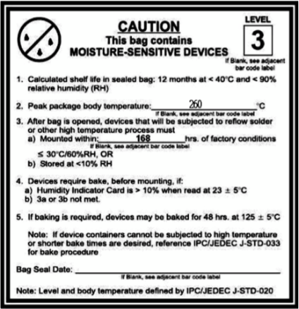
The stamp-hole module must be mounted by the SMT machine. After being unpacked, it must be soldered within 24 hours. Otherwise, it must be put into the drying cupboard where the RH is not greater than 10%, or it needs to be packaged under vacuum again and the exposure time needs to be recorded (the total exposure time cannot exceed 168 hours).
- SMT equipment:
- Mounter
- SPI
- Reflow soldering machine
- Oven temperature tester
- Automated optical inspection (AOI) equipment
- Baking equipment:
- Cabinet oven
- Anti-static heat-resistant pallets
- Anti-static heat-resistant gloves
- SMT equipment:
-
Storage conditions for a delivered module are as follows:
- The moisture-proof bag must be placed in an environment where the temperature is below 40°C and the relative humidity is lower than 90%.
- The shelf life of a dry-packaged product is 12 months from the date when the product is packaged and sealed.
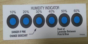
- The package contains a humidity indicator card (HIC).
-
The module needs to be baked in the following cases:
- Vacuum packing bag was found to be damaged before being unpacked.
- There is no humidity indicator card (HIC) in the vacuum packing bag.
- After being unpacked, 10% and above circles on the HIC become pink.
- The total exposure time has been more than 168 hours since unpacking.
- More than 12 months have passed since the sealing date of the bag.
-
Baking settings:
- Temperature: 60°C and ≤ 5%RH for reelizing and 125°C and ≤5%RH for palletizing (please use heat-resistant pallet rather than plastic pallet)
- Time: 48 hours for reelizing and 12 hours for palletizing
- Alarm temperature: 65°C for reelizing and 135°C for palletizing
- Production ready temperature after natural cooling: < 36°C
- The number of drying times: 1
- Re-baking condition: If a module remains unused for 168 hours after being unpacked, it must be baked again.
Important: If this batch of modules is not baked within 168 hours, do not use the wave soldering to solder them. Because these modules are 3-level moisture-sensitive components, they are very likely to get damp when exposed outside. In this case, if they are soldered at high temperatures, it may result in component failure or poor soldering.
-
In the whole production process, take electrostatic discharge (ESD) protective measures.
-
To guarantee the passing rate, it is recommended that you use the SPI and AOI to monitor the quality of solder paste printing and mounting.
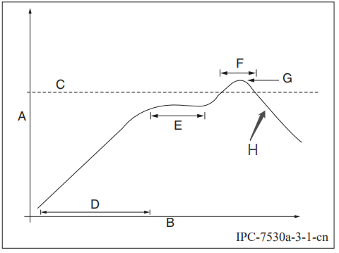
Recommended oven temperature curve
Perform mounting with the SMT based on the following reflow oven temperature curve. The highest temperature is 245°C. The reflow temperature curve is as below:
-
A: Temperature axis
-
B: Time axis
-
C: Liquidus temperature: 217 to 220°C
-
D: Ramp-up slope: 1 to 3°C/s
-
E: Duration of constant temperature: 60 to 120s; the range of constant temperature: 150 to 200°C
-
F: Duration above the liquidus: 50 to 70s
-
G: Peak temperature: 235 to 245°C
-
H: Ramp-down slope: 1 to 4°C/s
Note: The above curve is just an example of the solder paste SAC305. For more details about other solder pastes, please refer to Recommended oven temperature curve in the solder paste specifications.
Storage conditions
MOQ and packaging information
| Product number | MOQ (pcs) | Shipping packaging method | The number of modules per reel | The number of reels per carton |
|---|---|---|---|---|
| HPWSMS1 | Tape reel | 4 |
Appendix: Statement
FCC Caution: Any changes or modifications not expressly approved by the party responsible for compliance could void the user’s authority to operate this device.
This device complies with Part 15 of the FCC Rules. Operation is subject to the following two conditions: (1) This device may not cause harmful interference, and (2) this device must accept any interference received, including interference that may cause undesired operation.
Note: This device has been tested and found to comply with the limits for a Class B digital device, according to part 15 of the FCC Rules. These limits are designed to provide reasonable protection against harmful interference in a residential installation. This device generates, uses, and can radiate radio frequency energy and, if not installed and used following the instructions, may cause harmful interference to radio communications. However, there is no guarantee that interference will not occur in a particular installation.
If this device does cause harmful interference to radio or television reception, which can be determined by turning the device off and on, the user is encouraged to try to correct the interference by one or more of the following measures:
- Reorient or relocate the receiving antenna.
- Increase the separation between the device and receiver.
- Connect the device into an outlet on a circuit different from that to which the receiver is connected.
- Consult the dealer or an experienced radio/TV technician for help.
Radiation Exposure Statement
This device complies with FCC radiation exposure limits set forth for an uncontrolled rolled environment. This device should be installed and operated with a minimum distance of 20cm between the radiator and your body.
Important Note
This radio module must not be installed to co-locate and operating simultaneously with other radios in the host system except following FCC multi-transmitter product procedures. Additional testing and device authorization may be required to operate simultaneously with other radios.
The availability of some specific channels and/or operational frequency bands are country-dependent and are firmware programmed at the factory to match the intended destination. The firmware setting is not accessible by the end-user.
The host product manufacturer is responsible for compliance with any other FCC rules that apply to the host not covered by the modular transmitter grant of certification. The final host product still requires Part 15 Subpart B compliance testing with the modular transmitter installed.
The end-user manual shall include all required regulatory information/warnings as shown in this manual, including "This product must be installed and operated with a minimum distance of 20 cm between the radiator and user body".
This device has got an FCC ID: 2ANDL-HPWSMS1. The end product must be labeled in a visible area with the following: "Contains Transmitter Module FCC ID: 2ANDL-HPWSMS1".
This device is intended only for OEM integrators under the following conditions:
The antenna must be installed such that 20cm is maintained between the antenna and users, and the transmitter module may not be co-located with any other transmitter or antenna.
As long as the 2 conditions above are met, further transmitter tests will not be required. However, the OEM integrator is still responsible for testing their end-product for any additional compliance requirements required with this module installed.
Is this page helpful?
YesFeedbackIs this page helpful?
YesFeedback


