Application of DIP in Production
This topic describes the important notes and suggestions on the dual in-line package (DIP) for network modules. You can reduce the problems that might occur during production and improve the yield.
Scope of application
This topic is applicable to DIP packaging for network modules provided by Tuya.
References
-
Datasheets of network modules
-
J-STD-033 Handling, Packing, Shipping and Use of Moisture, Reflow, and Process Sensitive Devices
-
IPC-7530 Guidelines for Temperature Profiling for Mass Soldering Processes (Reflow & Wave)
Suggestions on motherboard design
-
Make sure the external frame of the module silk screen has accurate dimensions. Both ends or one end of the DIP module will be in vertical contact with the motherboard at 90 degrees, and no other components can be placed in this area.
-
We recommend that a module should be inserted from the top and surface-mount technology (SMT) components should not exceed 8 mm high at the bottom. Otherwise, wave soldering can only be implemented manually.
-
Do not place other components within 3 mm around the soldering area of the DIP module. The distance between the module soldering area and the edge of the board shall be greater than 3 mm. This way, the wave soldering fixture can be easily opened or manual soldering will not be affected.
-
Do not design the PCB as a mirror board, which is not suitable for wave soldering of the whole board.
-
The handling margin of the motherboard is recommended to be greater than 5 mm. The mark point is a solid circle with a diameter of 1 mm, and the center of the mark point is 4 mm away from the edge of the board. When the handling margin where the mark point is located is used as a conveyor belt, if the center of the mark point is less than 3.5 mm from the edge of the board, part of the mark point might be covered by the included side of the machine rail, and the machine is unable to recognize the mark point.
Confirm module before production
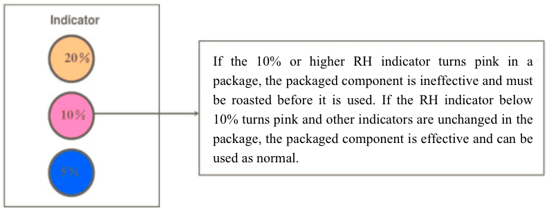
Check relative humidity indicator
Before production, open its vacuum package and check the relative humidity indicator. If the 10% or higher relative humidity indicator turns pink, as shown in the following figure, the component might be damp and must be baked before it is used.
Exposure duration of modules
Modules are Moisture Sensitivity Level-3 (MSL-3) humidity-sensitive components. After a module is unpacked, the module can be exposed to air for up to 168 hours. If it is exposed for more than 168 hours, it must be baked before you use it. In light of this, stick a label on the package of the module to record the time when it is unpacked. If the production is paused for over 24 hours after the module is unpacked, we recommend that you place the module in a moisture-proof box with a relative humidity level below 10%, or pack the module in vacuum again. Then, record the packing time and duration of exposure.
| MSL | Max duration of exposure to air Workshop environment ≤ 30°C/60%RH |
|---|---|
| MSL1 | Unlimited duration of exposure to air |
| MSL2 | 1 year |
| MSL2a | 4 weeks |
| MSL3 | 168 hours |
| MSL4 | 72 hours |
| MSL5 | 48 hours |
| MSL5a | 24 hours |
| MSL6 | Baking required before use |
Baking conditions
- For tape and reel packaging, the module is baked at a temperature of 40°C for 8 days.
- With a high-temperature resistant tray, the module is baked at a temperature of 125°C for 12 hours. The baking method with a high-temperature resistant tray packaging is recommended.
Suggestions on manual assembly with through hole technology (THT)
-
Incoming modules adopt tape and reel packaging. After unpacking, place the modules in a tray for assembly with THT. Avoid stacking modules and causing collisions and other defects. Special attention should be paid to modules mounted on both sides, such as LC5 series modules.
-
Modules are sensitive to static electricity. Before touching the modules, you must take electrostatic protection measures, and wear an anti-static wrist strap and gloves.
-
During assembly with THT, wave soldering fixtures and auxiliary tooling are recommended. This way, guarantee the verticality of the module after it is inserted into the motherboard, and thus improve the first pass yield of soldering.
Suggestions on wave soldering
-
Spray an appropriate amount of flux to all the positions that need to be soldered. However, components at the non-soldering surface cannot be sprayed with flux. For example, if spraying starts too early or ends too late, flux might be sprayed on areas that do not have PCBA.
-
The temperature setting meets the requirements of the recommended curve. A high temperature causes device damage, whereas a low temperature leads to poor soldering.
-
The wave height shall reach about two-thirds of the PCB height, but shall not exceed the upper surface of the PCB.
-
Clear away soldering dross every four hours, at least once every shift.
Suggestions on wave soldering fixtures
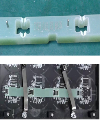
Batten
Insert the positioning hole on the batten into the positioning post on the wave soldering fixture. The module is positioned by two battens.
-
Strength: easy to operate and low cost.
-
Weakness: relatively low accuracy.
Clamping block
Cut out the shape of the upper part of the module on the clamping block, add positioning pins on the clamping block, and drill holes in the wave soldering fixture. When in use, align the slots of the clamping block with the module and put the module into the clamping block. And then, accurately insert the positioning pins into the positioning holes on the fixture, and use the module shape to fix the module.
-
Strength: high precision and low cost.
-
Weakness: slightly inconvenient operation.
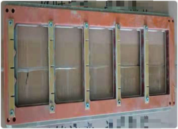
Cover plate
The cover plate is widely used in verticality control, component positioning, component clamping, and beyond. When controlling the module verticality, a module limit device is designed on the cover plate in the form of a slot or a fixed pin. Meanwhile, design positioning columns at the four corners to fix the cover plate, and add buckles at the two opposite corners to fasten the cover plate.
-
Strength: excellent precision, easy to operate, and high efficiency.
-
Weakness: high cost of fixtures.
Solder side of fixtures
The size of the window on the solder side must be appropriate. A small size results in insufficient soldering on the module, whereas a large size incurs unnecessary thermal shock to the PCB. The four sides of the fixture window should all be slanted. During wave soldering, tin can better contact the soldered pad and obtain better fluidity, reducing the probability of poor wave soldering.
Suggestions on the oven temperature
Refer to the oven temperature curve of wave soldering in the figure below and the oven temperature curve requirements in the table. During wave soldering, you shall adjust the oven temperature depending on the materials of other components and the PCB design.
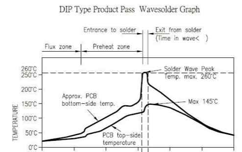
Suggestions on the oven temperature of wave soldering:
| Specification | Recommended value |
|---|---|
| Preheat temperature | 80°C to 130°C |
| Preheat duration | 75s to 100s |
| Contact duration at the peak | 3s to 5s |
| Solder tank temperature | 260 ± 5°C |
| Ramp-up slope | ≤ 2°C/s |
| Ramp-down slope | ≤ 6°C/s |
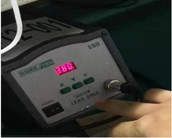
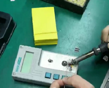
Suggestions on manual soldering
Make a special welding fixture to facilitate manual soldering operations and module fixation. Measure the temperature of soldering tools such as soldering irons and perform reliable grounding. Soldering operators must wear wired anti-static wrist straps.
| Specification | Recommended value |
|---|---|
| Soldering temperature | 360°C ± 20°C |
| Soldering duration | Less than 3s/point |
Is this page helpful?
YesFeedbackIs this page helpful?
YesFeedback


