Wi-Fi and Cellular Combo AI Voice Solution
Background information
Tuya Wi-Fi and cellular combo AI box is a voice interaction product developed using the Wi-Fi and Bluetooth combo module T5-E1-IPEX and the cellular module L511C-Y6E, both designed by Tuya Smart. This product integrates one microphone, one audio loopback channel, one speaker, one DIP switch, one function button, one optional external button, one eSIM card, and an NTC-enabled lithium battery.
Support major AI models including Doubao, DeepSeek, Qwen, OpenAI, and Gemini, featuring button wake-up, wake-word activation, and free conversation capabilities. This AI box delivers vivid and engaging AI voice interaction experiences.
Components
Main module T5-E1-IPEX
T5-E1-IPEX (T5 for short) is a highly integrated single-antenna single-band 2.4 GHz Wi-Fi 6 (IEEE 802.11b/g/n/ax) and Bluetooth 5.4 Low Energy (LE) combo IoT module. Featuring a multi-peripheral packaging and ultra-low-power chip, this module provides a highly integrated, secure, and lowest-power environment for IP cameras, HMI applications, smart locks, and other advanced IoT applications.
CPU and on-chip memory
- Built-in with Tuya’s custom T5QN88 chip, Armv8-M Star (M33F) processor, with a clock frequency of up to 480 MHz. The operating voltage range is 2.0V to 3.6V.
- 8 MB flash memory
- 16 MB PSRAM
- 640 KB shared SRAM
- 64 KB ROM
Wi-Fi features
- IEEE 802.11b/g/n/ax compliant
- 20 MHz and 40 MHz channel bandwidth
- Support downlink multi-user multiple input, multiple output (DL MU-MIMO)
- Support orthogonal frequency-division multiple access (OFDMA)
- Support target wake time (TWT)
- Integrated Bluetooth and Wi-Fi coexistence (packet traffic arbitration, PTA)
- Transmit (TX) power up to +20 dBm
- Receive (RX) sensitivity of -99 dBm
Bluetooth features
- Support Bluetooth Low Energy (LE) 5.4 standard
- Support Bluetooth LE 1 Mbit/s and long-range mode (125 Kbit/s and 500 Kbit/s)
- Transmit (TX) power of +6 dBm
- Receive (RX) sensitivity of -97 dBm
Cellular module L511C-Y6E
The L511C-Y6E module is a compact, high-reliability CAT.1BIS module featuring a 109-pin LCC+LGA package. It supports FDD/TDD communication modes with three low-power modes to flexibly address diverse power consumption requirements across scenarios. Also, the module supports FOTA, AT commands, and other features. Multiple interfaces and rich protocols, with multi-version USB drivers for simple and convenient applications, make it widely applicable in the IoT field.
Features
-
ARM Cortex-M3 processor, up to 204 MHz operating frequency
-
1 MB SRAM and 4 MB flash memory
-
Supported frequency bands
-
LTE-TDD: bands 34, 38, 39, 40, and 41
-
LTE-FDD: bands 1, 3, 5, and 8
-
-
Output power: 23 dBm ± 2 dBm
-
Comply with 3GPP R14 CAT.1BIS standard
-
Operating voltage range: 3.3V to 4.5V (3.8V recommended)
-
Low power
-
Idle mode (3 mA@3.8V)
-
Sleep mode (0.13 mA@3.8V)
-
Power-off mode: (1 μA@3.8V)
-
-
Transmission rate
-
LTE-FDD: Maximum download rate 10 Mbit/s, and maximum upload rate 5 Mbit/s
-
LTE-TDD: Maximum download rate 8.96 Mbit/s, and maximum upload rate 3.1 Mbit/s
-
Battery charging management chip ETA4056D2I
ETA4056D2I is a monolithic charging management IC for single-cell lithium batteries, featuring constant-current and constant-voltage charging modes. Designed for portable devices, this chip integrates thermal regulation, soft-start, and pre-charge features while eliminating the need for external current-sense resistors or blocking diodes, with a maximum 1.2A charge current.
Features
- 16V input isolation voltage
- 4.2V charge termination voltage
- 2.9V trickle charge threshold
- Charge current adjustable by external resistor, up to 1.2A
- BAT current as low as 250 nA when not charging
- NTC support
- Built-in soft start
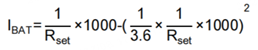
Buck chip ETA3485S2F
ETA3485S2F is a high-efficiency DC-DC buck converter with up to 96% efficiency. It is capable of delivering a maximum output current of 1.5A. It supports an input voltage range of 2.6V–7V, with an adjustable output voltage range of 0.6V–VIN, making it ideal for low-voltage power conversion applications.~~
Features
- High efficiency up to 96%
- Fixed switching frequency of 2 MHz
- Built-in soft-start control circuit
- Short-circuit protection and over-temperature protection
Audio amplifier CS8302M
CS8302M is a high-efficiency, ultra-low EMI 3.0W mono Class D audio amplifier featuring proprietary Adaptive Edge Rate Control (AERC) technology. It can deliver superior full-bandwidth EMI suppression, making it ideal for EMI-sensitive applications such as FM radio, CMMB, and analog mobile TV. The chip has built-in over-current protection, short-circuit protection, and over-temperature protection, which can effectively protect the chip from being damaged under abnormal working conditions.
Features
- Operating voltage range: 2.5V to 6.0V
- Filterless Class-D structure
- High efficiency up to 90%
- High power supply rejection ratio
- 40 ms startup time
- 3 mA quiescent current and less than 0.1 μA shutdown current
Hardware design specifications
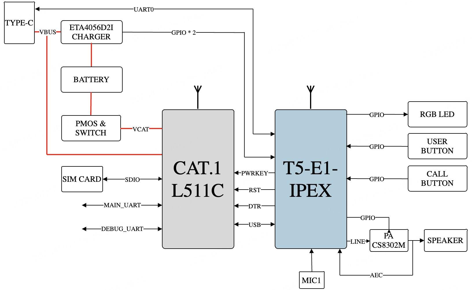
The functional block diagram and power tree of the Wi-Fi and cellular combo AI box are as follows:
Functional block diagram
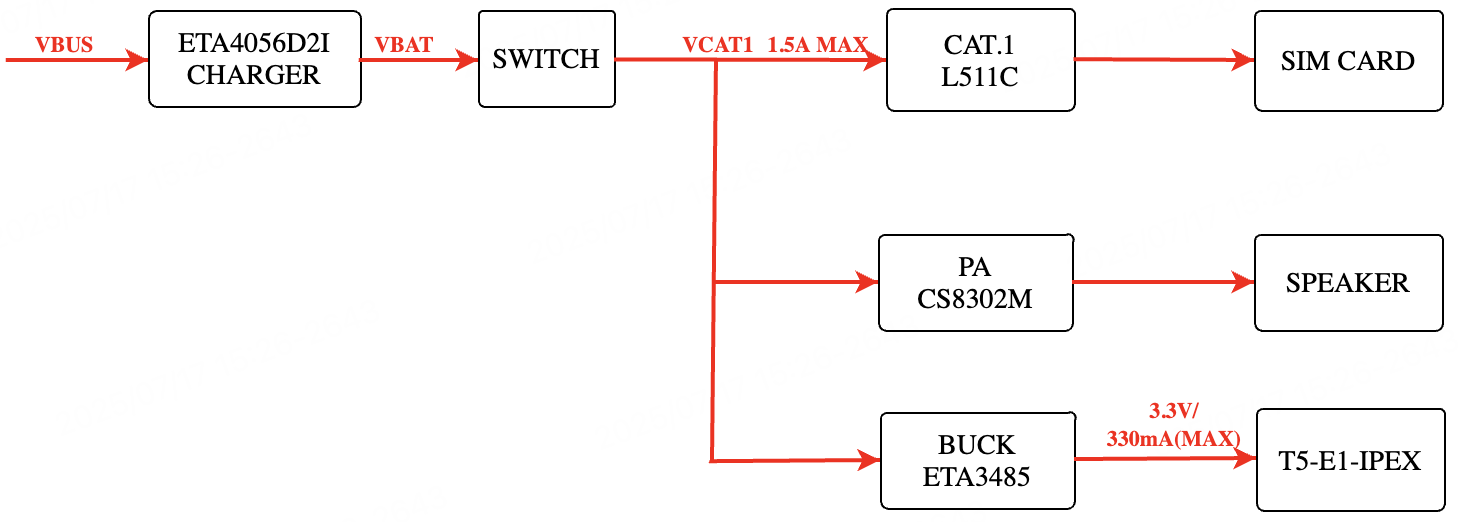
Power tree
Schematic diagram
Power circuit
The VBUS input passes through the 0R protection resistor, TVS, and filter capacitor, and then charges the battery through the battery charging management chip. A PMOS (P-channel MOSFET) is connected in series between the battery output and the downstream main power path. The on/off state of the PMOS is controlled by a DIP switch. Both the cellular module and audio amplifier operate in the battery voltage domain, while the T5 module uses a 3.3V voltage domain.
-
Type-C circuit:
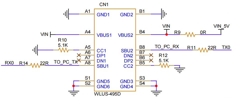
Type-C CC1 and CC2 pins are each grounded through 5.1 kΩ resistors to ensure the device always operates as a upstream facing port (UFP), preventing power-on failures when connected to fast-charge adapters. SBU1 and SBU2 are connected to the T5 module’s
UART0via series resistors, enabling direct firmware flashing, authorization, and production testing through the Type-C port. -
Battery charging and discharging circuit:
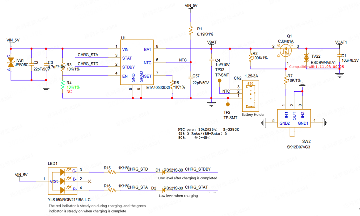
The charging management chip ETA4056D2I features a 4.2V charge termination voltage. TVS1 is used to suppress power surge voltage to protect the charging management chip, and R5 sets the resistance for the charging current. Adjust the parameters according to the actual battery usage. Refer to the figure below for the calculation formula:
-
With a 1 kΩ resistor, the charging current is approximately 920 mA. With a 2 kΩ resistor, it drops to around 480 mA. LED1 indicates battery state: red during charging and green when complete. R1 and C57 must be matched to the lithium battery’s NTC specifications. The shown values are optimized for a 10 kΩ@25°C (B=3380K) NTC, supporting a charging temperature range of 0–45°C.
-
SW2 is a DIP switch controlling the on/off state of VCAT1. When SW1 is toggled to the Pin 1 side, Q1 conducts, setting VCAT1 to VBAT voltage. When SW1 is toggled to the Pin 3 side, Q1 turns off, cutting off VCAT1 output.
-
-
Buck circuit:
Buck circuit ETA3485S2F is used. R8 and R13 set the output voltage, while feedforward capacitor C10 improves power supply dynamic response. C5, C6 (input) and C7, C8, C9 (output) serve as filter capacitors for the buck converter. Power inductor L1 must have a saturation current rating that meets the product’s actual requirements. The 3.3V output supplies the T5 module via magnetic bead FB1, which suppresses high-frequency noise and spike interference on the power line.
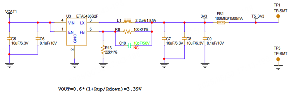
Circuit of cellular module
-
CAT.1 circuit:
Cellular module L511C-Y6E is used. The module power shares the same voltage domain as the battery, with large and small capacitors connected in parallel on the power line. The large capacitor enhances instantaneous high-current handling capability, while the small capacitor provides bypassing to filter out high-frequency noise from the power supply.
- The module’s PWRKEY pin has a ground-terminated resistor R21 and connects to pin 16 of the T5 module via D3 to control the cellular module’s power-on/off operation.
- The cellular module’s reset pin connects to the T5 module’s Pin 8 via D4. Applying a low-level signal lasting over 100 ms to this pin triggers a reset and reboot of the cellular module.
- The cellular module and T5 module communicate via USB, where
USB_VBUSserves as the USB insertion detection pin. This line is paralleled with 1 μF and 22 pF filter capacitors. The pin is controlled by a switching circuit composed of Q2 and Q3 from the T5 module. Therefore, the cellular module can be woken from sleep for USB communication.
The cellular module’s antenna pad Pin 35 connects to both an IPEX antenna connector and a pogo pin through a π-type matching circuit composed of C22, R19, and C23 (parameters to be adjusted based on final product testing). The specific antenna implementation depends on the mechanical design. Pay attention to the pogo pin plunger height and mechanical compatibility to ensure proper contact after assembly.
-
MAIN_UARTserves as a full-featured serial port with test points connected through series resistors. -
MAIN_DTRis connected to Pin 33 of the T5 module via a series resistor, reserved as a channel for the T5 module to wake up the cellular module. -
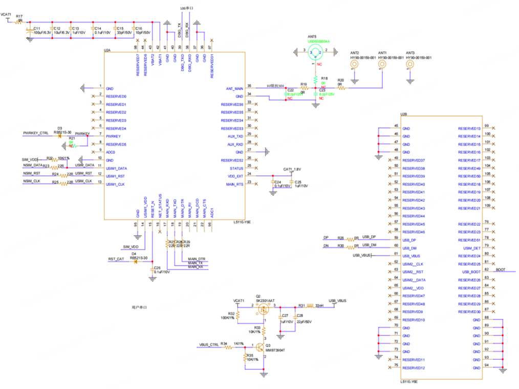
SIM card circuit:
Due to product size constraints, the SIM card adopts a USIM package soldered directly onto the PCB. A parallel combination of 0.1 μF and 33 pF capacitors is placed between power and GND for filtering and bypassing. Moreover, 33 pF capacitors are connected to ground on all SIM card signal and clock lines to eliminate high-frequency interference.
For more information, see the L511C-Y6E Module Datasheet.
T5 module circuit
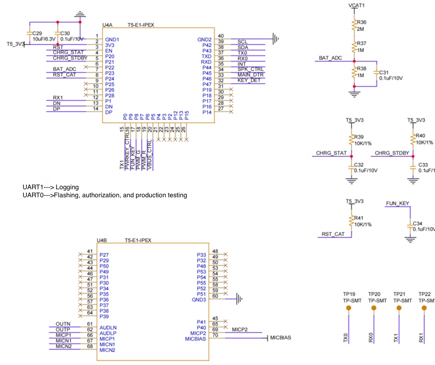
The T5 module serves as the main controller (with BAT_ADC reserved for lithium battery voltage detection and remaining capacity estimation):
CHRG_STATandCHRG_STDBYdetermine battery charging status.FUN_KEYandKEY_DETdetect button inputs.PWM_RandPWM_Gcontrol the on/off states of the red/green LED.UART0is used for flashing, authorization, and production testing, accessible via the Type-C connector.UART1is a reserved test point of the logging UART.SCL,SDA, andINTare reserved for GSENSOR sensor interfacing.SPK_CTRLis the audio amplifier enable signal (active high).MIC1connects to an external microphone for audio capture, whileMIC2is used for audio loopback (echo cancellation). The audio signal is amplified by the audio amplifier and output with a speaker for voice playback.
For more information, see the T5-E1-IPEX Module Datasheet.
Button and LED circuit
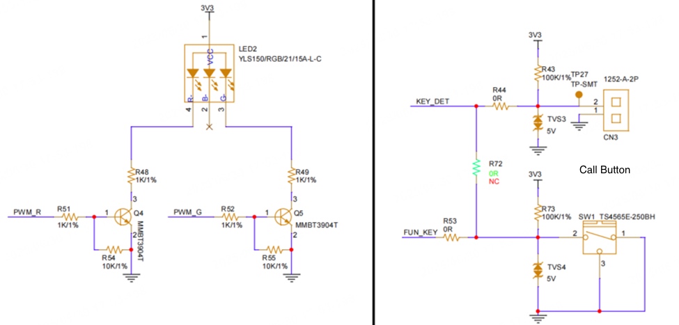
The RGB LED (LED2) utilizes red and green colors to indicate different device operational states. R48 and R49 are current-limiting resistors (values adjustable based on product requirements).
You can define the functions of the onboard button SW1 and the external button CN3. To accommodate varying button configurations across different mechanical designs, the two button signals are interconnected via resistor R72. Optional soldering is applied based on project requirements during actual implementation.
Audio circuit
Microphone and speaker circuit
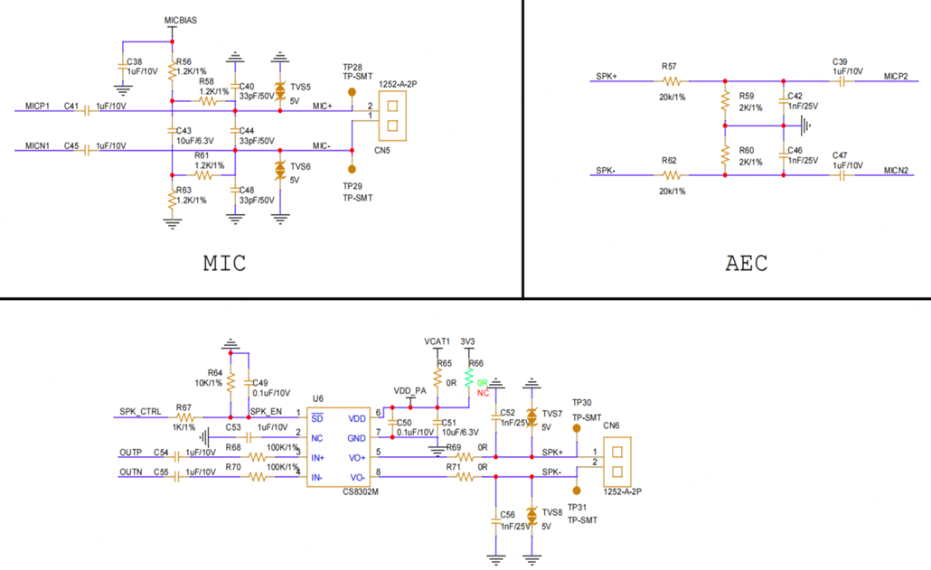
The audio circuit is shown in the diagram. MIC_BIAS provides a microphone bias voltage, with C38 filtering power supply noise. R56, R58, R61, and R63 serve as bias resistors. C40, C44, and C48 filter interference signals. C41 and C45 are DC-blocking capacitors that remove DC components from the microphone signal. TVS5 and TVS6 provide electrostatic discharge (ESD) protection for the microphone inputs. In the AEC circuit, the power amplifier’s output signal is divided and filtered through R57/R59/C42 and R62/R60/C46, and then fed into the T5 module’s MIC2 interface via DC-blocking capacitors C39 and C47 for echo cancellation.
The audio amplifier is powered directly using VCAT1. C50 and C51 decouple the power supply, while the enable pin is pulled down via R64 to ensure the circuit remains off after power-up. C54, C55, R68, and R70 set the high-pass filter cutoff frequency and gain (3x amplification in this configuration). The output path components (R69, R71, C52, and C56) suppress noise and improve signal quality.
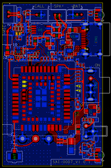
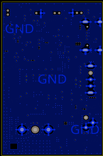
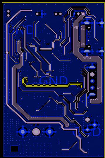
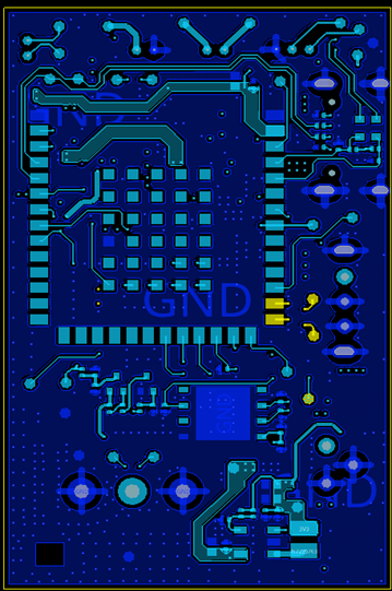
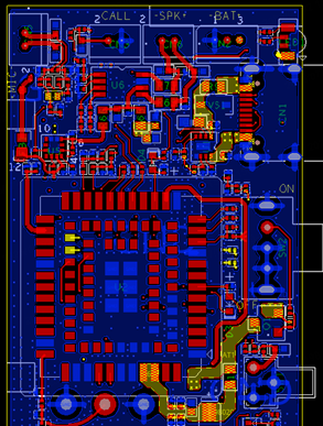
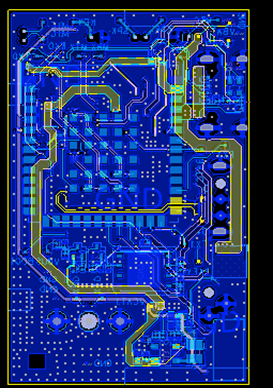
PCB
Layout reference
The PCB is composed of 4 layers. From top to bottom, they are the top layer, GND layer, SIG layer, and bottom layer. The trace of each layer is shown in the figure below:
Trace requirements
-
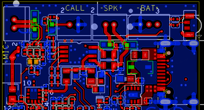
Structural components, such as Type-C connectors, DIP switches, buttons, and LEDs, must be placed as required to avoid interference.
-
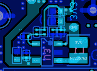
In the buck circuit, place the input and output capacitors as close as possible to VCAT1 and GND. The SW trace should be short and thick to improve the overcurrent capability. The feedback resistor should be placed as close as possible to the chip feedback pin, and the feedback voltage should be sourced from the output capacitor.
-
Power trace width must meet maximum current-carrying requirements, such as 5V power input, battery charge/discharge circuits, cellular module power supply, T5 module power supply, and audio amplifier power traces. Sufficient vias must be added when changing layers to enhance current-carrying capacity.
-
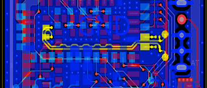
Decoupling capacitors for chip power supplies should be placed as close as possible to their corresponding pins. Traces are routed to ensure the power passes through the capacitors for filtering before entering the chip. Examples include the decoupling capacitors for the power supplies of the CAT.1 cellular module, SIM card, and buck chip, as shown in the diagram.
-
USB data lines must be routed as differential pairs with controlled 90Ω impedance, isolated from other signals using ground traces. RF traces should be as short as possible with controlled 50Ω impedance, wrapped with copper foil and accompanied by evenly spaced ground vias along the route. Minimize component placement near RF connectors and maintain ground plane integrity in their vicinity.
-
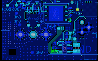
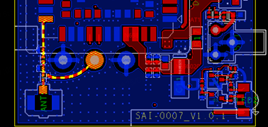
All protection devices must be placed close to the signal input ports. Traces are routed to pass through the protection components before entering the chip internals, as illustrated in the diagram below.
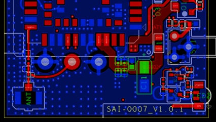
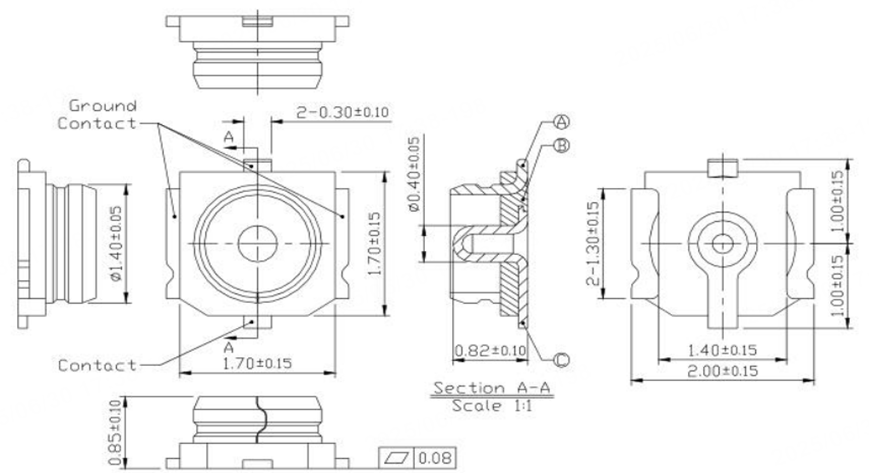
Antenna connector for T5 module
Structural design specifications
Structural design depends on the actual product form. To ensure optimal echo cancellation, it is recommended to maximize the distance between the speaker and the microphone and mount them on different reference planes.
Reference bill of materials (BOM)
Contact your product manager offline to obtain the BOM.
SDK development guide
For more information, see Wukong AI Hardware Development Framework.
Is this page helpful?
YesFeedbackIs this page helpful?
YesFeedback


