L511(C/E/A/J)-Y6(E) Module Datasheet
Overview
The L511-Y6 series is a Cat.1bis module with small packaging, stable and reliable performance, and LCC+LGA. It can well meet customers’ requirements for high cost-effectiveness and low power consumption, and can be widely used in the IoT field. For example, in public network intercom, mobile payment, security, in-car DTU, and fields such as asset tracking and sharing economy.
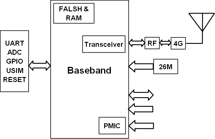
System module diagram
Main characteristics
-
Processor
ARM Cortex-M3@204M Hz -
Memory
L511C-Y6// L511E-Y6/L511A-Y6/L511J-Y6: 1 MB SRAM+2MB Flash
L511C-Y6E/L511E-Y6E: 1MB SRAM+4MB Flash -
Supporting frequency bands
L511C-Y6/L511C-Y6E:
TDD-LTE: B34/B38/B39/B40/B41
FDD-LTE: B1/B3/B5/B8
L511E-Y6/L511E-Y6E:
TDD-LTE: B38/B40/B8
FDD-LTE: B1/B3/B5/B7/B8/B20/B28
L511A-Y6:
FDD-LTE: B2/B4/B5/B12/B13/B66/B71
L511J-Y6:
TDD-LTE: B39/B41
FDD-LTE: B1/B3/B8/B18/B19/B26/B28 -
Output power
LTE: 23 dBm±2Db -
Receiving sensitivity
Refer to Reception sensitivity.
-
Data transmission
LTE-FDD: Maximum downlink speed of 10Mbps, maximum uplink speed of 5Mbps
LTE-TDD: Maximum downlink speed 8.96Mbps, maximum uplink speed 3.1Mbps -
Ultra-low power consumption
LTE Standby: 0.98mA @3.8V/AT+ECPMUCFG=1,2 -
Support Wi-Fi scan function
Product specifications
- Working voltage: 3.3-4.5 V (recommended 3.8 V)
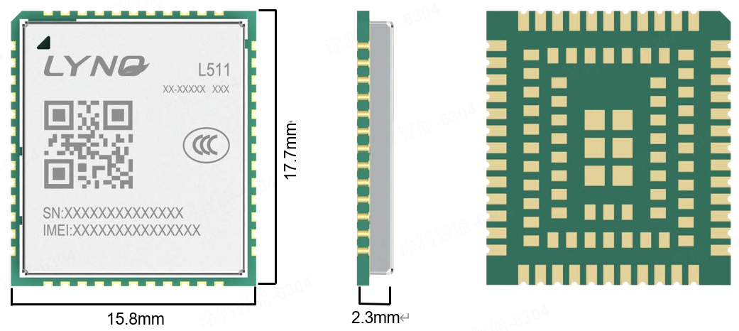
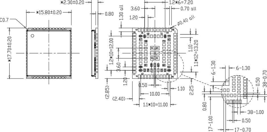
- Size: 15.8mm * 17.7mm * 2.3mm
- 109 -pin LCC+LGA
- Working temperature: -40°C to +85°C
- Storage temperature: -45°C to +90°C
- Weight: Approximately 1.12 grams
Interface
- GPIO
- USB 2.0 interface
- ADC
- (U) SIM card (1.8V/3.0V)
- UART
- Key
- Antenna interface
Comparison of module differences
Comparison of Differences between L511-Y6 Series
| Module | Flash | Frequency band |
|---|---|---|
| L511C-Y6 | 1MB SRAM+2MB Flash | TDD-LTE: B34/B38/B39/B40/B41 FDD-LTE: B1/B3/B5/B8 |
| L511C-Y6M | 1MB SRAM+2MB Flash | TDD-LTE: B34/B38/B39/B40/B41 |
| L511E-Y6 | 1MB SRAM+2MB Flash | TDD-LTE: B38/B40/B41 FDD-LTE: B1/B3/B5/B7/B8/B20/B28 |
| L511E-Y6E | 1MB SRAM+4MB Flash | TDD-LTE: B38/B40/B41 FDD-LTE: B1/B3/B5/B7/B8/B20/B28 |
| L511A-Y6 | 1MB SRAM+2MB Flash | FDD-LTE: B2/B4/B5/B12/B13/B66/B71 |
| L511J-Y6 | 1MB SRAM+2MB Flash | TDD-LTE: B39/B41 FDD-LTE: B1/B3/B8/B18/B19/B26/B28 |
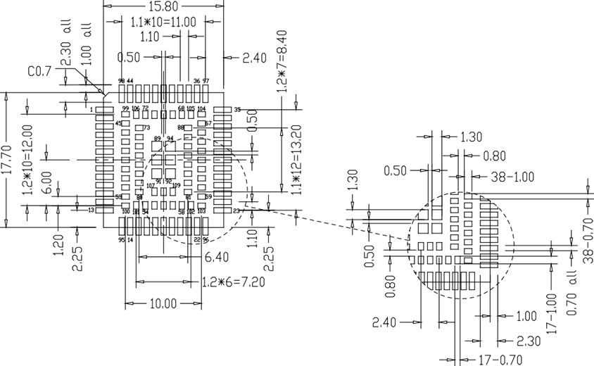
Module pin definition
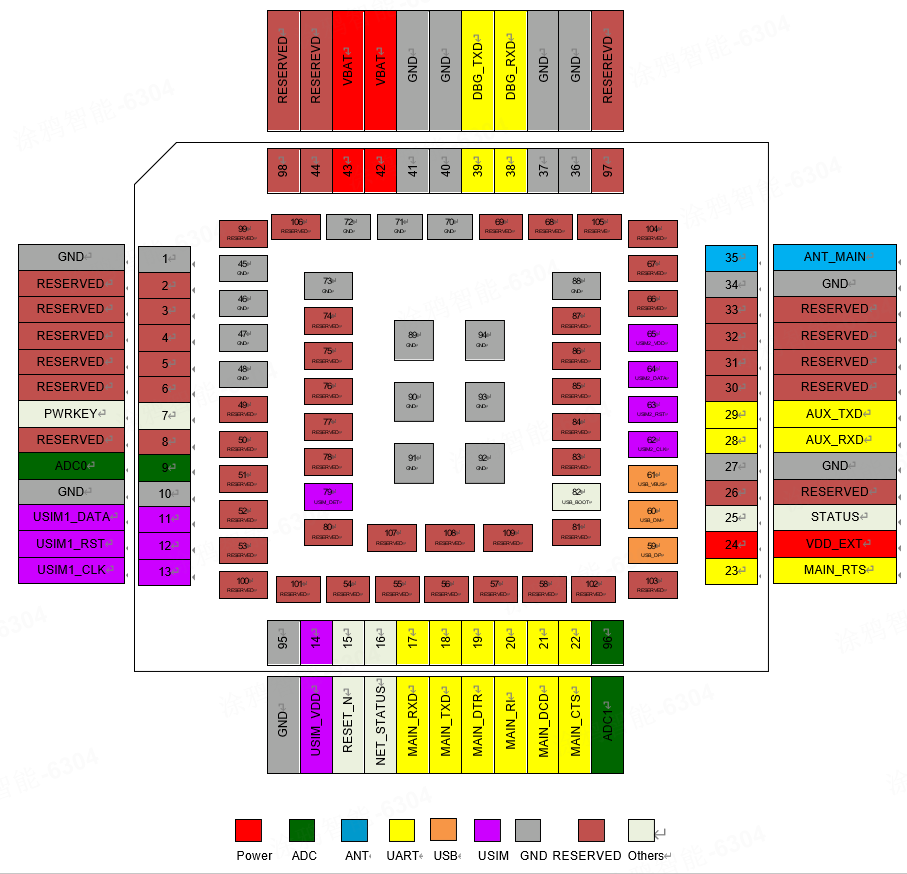
Pin distribution diagram
Pin distribution of L511-Y6 series (top view)
Module pin description
The L511-Y6 series has a total of 109 pins, and the specific interface functions and series pin descriptions are as follows.
| Pin | Pin name | Mode | Function description | Voltage domain | Status (1) |
|---|---|---|---|---|---|
| LCC PIN | |||||
| 1. | GND | G | Ground | - | GND |
| 2. | RESERVED | - | Not connect | - | - |
| 3. | RESERVED | - | Not connect | - | - |
| 4. | RESERVED | - | Not connect | - | - |
| 5. | RESERVED | - | Not connect | - | - |
| 6. | RESERVED | - | Not connect | - | - |
| 7. | PWRKEY | DI | Power key button | 1.8 to 2.2V | Open |
| 8. | RESERVED | - | Not connect | - | - |
| 9. | ADC0 | AI | ADC | External input channel 0 , 12bit | 0.05 to 1.2V |
| 10. | GND | G | Ground | - | GND |
| 11. | USIM1_DATA | DIO | USIM1 data | 1.8V/3.0V | Open |
| 12. | USIM1_RST | DO | USIM1 reset | 1.8V/3.0V | Open |
| 13. | USIM1_CLK | DO | USIM1 clock | 1.8V/3.0V | Open |
| 95. | GND | G | Ground | - | GND |
| 14. | USIM1_VDD | PO | USIM1 output voltage | 1.8V/3.0V | Open |
| 15. | RESET_N | DI | System reset signal | 1.28V | Open |
| 16. | NET_STATUS | DO | Output PIN as LED control for network status | 1.8V | Open |
| 17. | MAIN_RXD | DI | Main UART receive data input | 1.8V | Open |
| 18. | MAIN_TXD | DO | Main UART transmit data output | 1.8V | Open |
| 19. | MAIN_DTR | DI | Main UART data terminal ready | 1.2V | Open |
| 20. | MAIN_RI | DO | Main UART ring indicator | 1.8V | Open |
| 21. | MAIN_DCD | DO | Main UART data carrier detect | 1.8V | Open |
| 22. | MAIN_CTS | DO | Main UART clear to send | 1.8V | Open |
| 96. | ADC1 | AI | ADC1 external input channel , 12bit | 0.05 to 1.2V | Open |
| 23. | MAIN_RTS | DI | Main UART request to send | 1.8V | Open |
| 24. | VDD_EXT | PO | 1.8V output voltage, output current up to 2mA | 1.8V | Open |
| 25. | STATUS | DO | Output indicating of module PIN as operating status | 1.8V | Open |
| 26. | RESERVED | - | Not connect | - | - |
| 27. | GND | G | Ground | - | GND |
| 28. | AUX_RXD | DI | Auxiliary UART receive data input | 1.8V | Open |
| 29. | AUX_TXD | DO | Auxiliary UART transmit data output | 1.8V | Open |
| 30. | RESERVED | - | Not connect | Open | - |
| 31. | RESERVED | - | Not connect | Open | - |
| 32. | RESERVED | - | Not connect | Open | - |
| 33. | RESERVED | - | Not connect | Open | - |
| 34. | GND | G | Ground | - | GND |
| 35. | ANT_MAIN | ANT Main Antenna | Open | - | - |
| 97. | RESERVED | - | Not connect | ||
| 36. | GND | G | Ground | - | GND |
| 37. | GND | G | Ground | - | GND |
| 38. | DBG_RXD | DI | Debug UART receive data input | 1.8V | Open |
| 39. | DBG_TXD | DO | Debug UART transmit data output | 1.8V | Open |
| 40. | GND | G | Ground | - | GND |
| 41. | GND | G | Ground | - | GND |
| 42. | VBAT | PI | Power supply | 3.3 to 4.5V | VBAT |
| 43. | VBAT | PI | Power supply | 3.3 to 4.5V | VBAT |
| 44. | RESERVED | - | Not connect | - | - |
| 98. | RESERVED | - | Not connect | - | - |
| LGA PIN | |||||
| 45. | GND | G | Ground | - | GND |
| 46. | GND | G | Ground | - | GND |
| 47. | GND | G | Ground | - | GND |
| 48. | GND | G | Ground | - | GND |
| 49. | RESERVED | - | Not connect | - | - |
| 50. | RESERVED | - | Not connect | - | - |
| 51. | RESERVED | - | Not connect | - | - |
| 52. | RESERVED | - | Not connect | - | - |
| 53. | RESERVED | - | Not connect | - | - |
| 54. | RESERVED | - | Not connect | - | - |
| 55. | RESERVED | - | Not connect | - | - |
| 56. | RESERVED | - | Not connect | - | - |
| 57. | RESERVED | - | Not connect | - | - |
| 58. | RESERVED | - | Not connect | - | - |
| 59. | USB_DP | IO | USB | port differential data line | Open |
| 60. | USB_DM | IO | USB | port differential data line | Open |
| 61. | USB_VBUS | PI | USB 5V voltage input | 5V | Open |
| 62. | USIM2_CLK | DO | USIM2 clock | 1.8V | Open |
| 63. | USIM2_RST | DO | USIM2 reset | 1.8V | Open |
| 64. | USIM2_DATA | DIO | USIM2 data | 1.8V | Open |
| 65. | USIM2_VDD | PO | USIM2 output voltage | 1.8V | Open |
| 66. | RESERVED | - | Not connect | - | - |
| 67. | RESERVED | - | Not connect | - | - |
| 68. | RESERVED | - | Not connect | - | - |
| 69. | RESERVED | - | Not connect | - | - |
| 70. | GND | G | Ground | - | GND |
| 71. | GND | G | Ground | - | GND |
| 72. | GND | G | Ground | - | GND |
| 73. | GND | G | Ground | - | GND |
| 74. | RESERVED | - | Not connect | - | - |
| 75. | RESERVED | - | Not connect | - | - |
| 76. | RESERVED | - | Not connect | - | - |
| 77. | RESERVED | - | Not connect | - | - |
| 78. | RESERVED | - | Not connect | - | - |
| 79. | USIM1_DET | DI | USIM1 detect pin | 1.2V | Open |
| 80. | RESERVED | - | Not connect | - | - |
| 81. | RESERVED | - | Not connect | - | - |
| 82. | USB_BOOT | DI | Force software download | 1.8V | Open |
| 83. | RESERVED | - | Not connect | - | - |
| 84. | RESERVED | - | Not connect | - | - |
| 85. | RESERVED | - | Not connect | - | - |
| 86. | RESERVED | - | Not connect | - | - |
| 87. | RESERVED | - | Not connect | - | - |
| 88. | GND | G | Ground | - | GND |
| 89. | GND | G | Ground | - | GND |
| 90. | GND | G | Ground | - | GND |
| 91. | GND | G | Ground | - | GND |
| 92. | GND | G | Ground | - | GND |
| 93. | GND | G | Ground | - | GND |
| 94. | GND | G | Ground | - | GND |
| 99. | RESERVED | - | Not connect | - | - |
| 100. | RESERVED | - | Not connect | - | - |
| 101. | RESERVED | - | Not connect | - | - |
| 102. | RESERVED | - | Not connect | - | - |
| 103. | RESERVED | - | Not connect | - | - |
| 104. | RESERVED | - | Not connect | - | - |
| 105. | RESERVED | - | Not connect | - | - |
| 106. | RESERVED | - | Not connect | - | - |
| 107. | RESERVED | - | Not connect | - | - |
| 108. | RESERVED | - | Not connect | - | - |
| 109. | RESERVED | - | Not connect | - | - |
(1) Suggested status when not in use.
- The VDD_EXT of the L511-Y6 series can maintain an output of 1.8V during sleep; The voltage domain of the remaining 1.8V interfaces will be turned off during module sleep, MAIN_DTR can function normally when the module is in sleep mode.
- The USB-BOOT (PIN82) pin of the L511-Y6 series is prohibited from being pulled up to a high level until the module is successfully powered on.
- If the module has enabled the AT serial port wake-up function, the voltage domain of the MAIN_RXD signal will become 1.1V after the module goes to sleep.
Pin type description
| Pin | Description |
|---|---|
| PI | Power input |
| PO | Power output |
| DI | Digital input |
| DO | Digital output |
| IO | Input/output |
| AI | Analog input |
| ANT | Antenna |
| G | Ground |
Module encapsulation information
Module structure dimensions
The front view, back view, and side view of the module’s peripheral dimension information are shown in the following figure.
Product label
L511-Y6 series labels
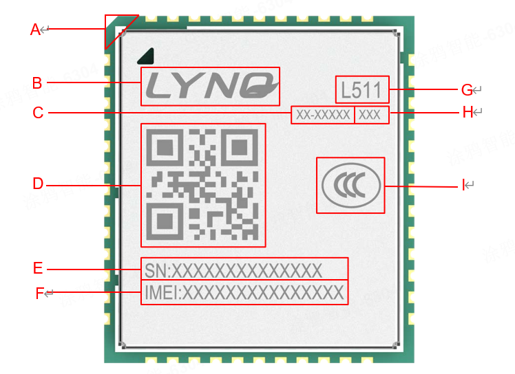
Tag description
| Code | Description |
|---|---|
| A | Pin1 foot |
| B | Company Logo |
| C | Finished product part number of module |
| D | QR code - including IMEI number and SN number |
| E | SN number |
| F | IMEI number |
| G | Module Name |
| H | Module configuration |
| I | 3C certification |
Module packaging size (unit: mm)
Recommended solder pads for module packaging (unit: mm)
Interface circuit reference design
Power supply section
Power supply
VBAT is the main power supply for the module, with a voltage input range of 3.3V to 4.5V, and a recommended voltage of 3.8V. In poor network environments, the antenna will transmit at maximum power. To ensure power stability, the module must choose a power supply that can provide at least 1.2A current capability. It is recommended to use a 100uF filtering capacitor with low ESR (ESR=0.7 ohms) near the VBAT pin of the module. At the same time, it is recommended to add at least 3 (100nF, 33pF, 10pF) multi-layer ceramic capacitors (MLCC) with the best ESR performance to VBAT and place the capacitors near the VBAT pin.
When connecting the external power supply module, VBAT needs to use star-shaped wiring. The width of VBAT wiring should not be less than 1.2mm, and in principle, the longer the VBAT wiring, the wider the required line width. In addition, to ensure power stability, it is recommended to add a TVS tube with VRWM=4.7V and PPP ≥ 500W at the front end of the power supply.
Power interface circuit

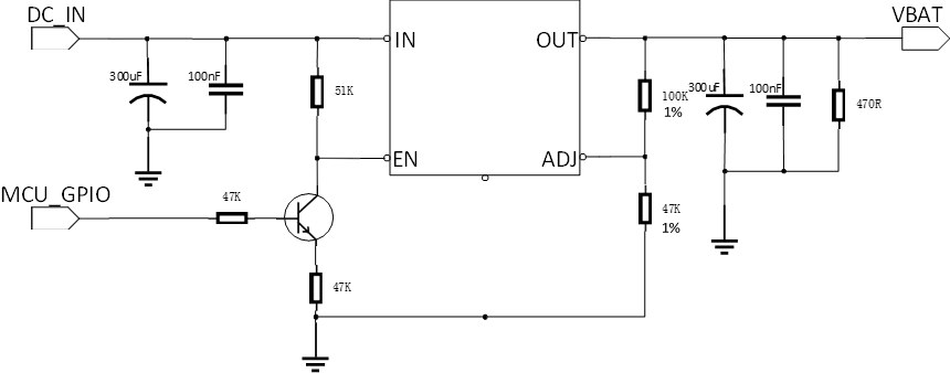
In the absence of a network, the RTC clock error of the module is relatively large, with several minutes of error in 24 hours. To obtain accurate time, it is necessary to synchronize the network’s time.
If the voltage difference is not very large, the LDO power supply scheme can be used, as shown in the following figure using the LDO power supply circuit as a reference. The LDO requires an overcurrent capability of 1.2A or above, but due to its linear voltage reduction, its transient response capability is poor, and a large number of capacitors need to be equipped at the front and rear ends to prevent possible reset or shutdown caused by excessive voltage fluctuations during high-power transmission. The output voltage needs to be controlled at 3.8V.
LDO power supply circuit
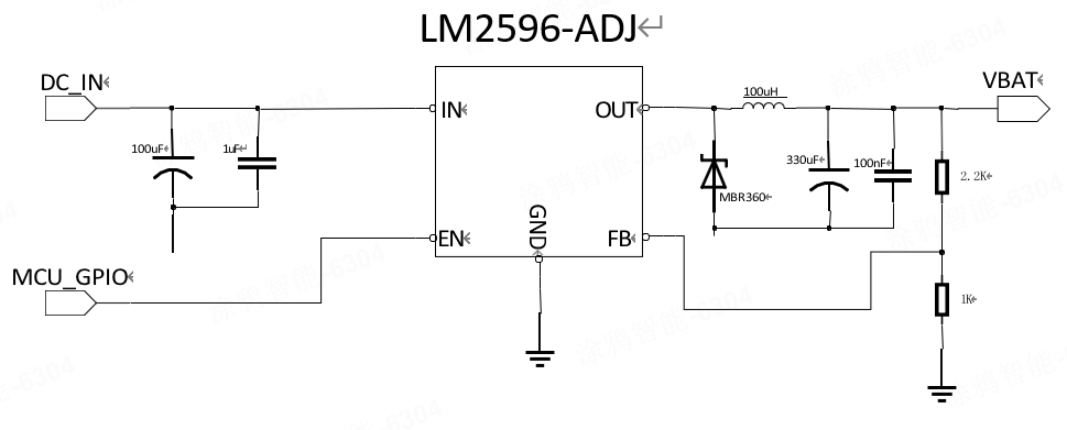
If the voltage difference is relatively large, it is recommended to use DC/DC, with an output current requirement of 1.2A or above. As shown in the figure below, a DC/DC switching power supply is used, supplemented by large capacity capacitors (above 330uF), to ensure the normal operation of the RF PA (power amplifier). The advantage of this reference design is that it can provide good transient current response, meet the requirements of module operation under weak signals, and prevent network failure or port restart caused by insufficient power supply.
DC/DC power supply circuit
Hardware startup
The 7th pin of the module is the hardware boot input terminal, which can be powered on through the PWRKEY pin when the module is powered on. Pull down the PWRKEY pin for more than 1 second and then release it to power on the module. There is a pull-up inside the module, with a Typical value of 1.8-2.2 V.
There are two ways to shut down a module:
- Using the AT command AT+POWEROFF, the shutdown process takes about 3 seconds to complete.
- Pull down PWRKEY for more than 3 seconds and then release to achieve shutdown.
Power button
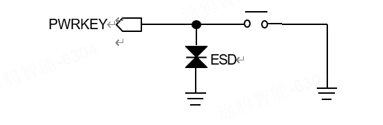
If power on is required, it is recommended to pull the PWRKEY down to the ground through a 0R resistor and ensure that the starting voltage for VBAT power on is less than 0.5V.
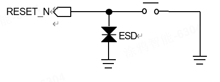
Hardware reset
The 15th pin of the module is the hardware reset input terminal, and there is a weak pull-up inside the system, which defaults to a high level. When a low-level trigger reset is applied to the pin for 100ms, the module will restart. The Typical value is 1.28 V, which can be directly connected to the GPIO port of MCU ranging from 1.8V to 3.3V.
System reset button
(U) SIM card
Pin description
The L511-Y6 series module supports dual (U) SIM card function and only supports dual card single standby. The module’s (U) SIM 1 card (pin numbers: 11, 12, 13, 14) supports and can automatically detect 1.8V and 3.0V (U) SIM cards, while the (U) SIM 2 card (pin numbers: 62, 63, 64, 65) only supports 1.8V (U) SIM card detection. The (U) SIM card interface signal is shown in Table 3.2.1-1.
(U) Definition and Explanation of SIM Card Signal
| Pin | Signal name | Signal definition | Signal description |
|---|---|---|---|
| 11 | USIM1-DATA | (U) SIM 1 card data pin | (U) SIM 1 card data signal, bidirectional signal |
| 12 | USIM1-RST | (U) SIM 1 card reset pin | (U) SIM 1 card reset signal, output by the module |
| 13 | USIM1_CLK | (U) SIM 1 card clock pin | (U) SIM 1 card clock signal, output by the module |
| 14 | USIM1-VDD | (U) SIM 1 card power supply | (U) SIM 1 card power supply, output by the module |
| 79 | USIM1-DET | (U) SIM 1 card hot plug detection pin | (U) SIM 1 card hot plug detection signal, input signal |
| 62 | USIM2_CLK | (U) SIM 2 card clock pin | (U) SIM 2 card clock signal, output by the module |
| 63 | USIM2-RST | (U) SIM 2 card reset pin | (U) SIM 2 card reset signal, output by the module |
| 64 | USIM2-DATA | (U) SIM 2 data pin | (U) SIM 2 data signal, bidirectional signal |
| 65 | USIM2-VDD | (U) SIM 2-card power supply | (U) SIM 2-card power supply, output by module |
(U) SIM card interface application
(U) The SIM 1 card signal group (pin numbers: 11, 12, 13, 14) and the (U) SIM 2 card signal group (pin numbers: 62, 63, 64, 65) need to be designed with ESD protection devices near the (U) SIM card socket.
In order to meet the requirements of 3GPP TS 27.005 protocol and EMC certification, it is recommended to arrange the (U) SIM card slot near the module (U) SIM card interface to avoid severe waveform deformation and signal integrity caused by excessively long wiring. The routing of USIM.CLK and USIM.DATA signal lines must be protected by grounding. Connect a 1uF capacitor in parallel between USIM.VDD and GND to filter out interference from RF signals. It is recommended to add a 20K pull-up resistor to USIM.VDD for USIM.DATA signals.
(U) SIM card signal connection circuit
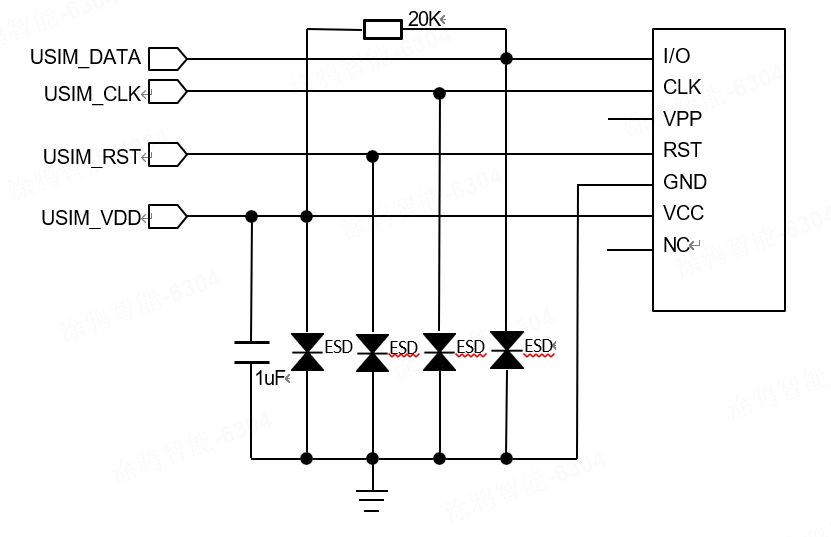
The recommended capacitance value for ESD devices is less than 22pF. If you want to use the hot plug function of the (U) SIM card, you need to choose a (U) SIM card holder with a hot plug detection PIN.
USB interface
Pin description
The USB interface of the module complies with the USB 2.0 specification and electrical characteristics. Supports two working modes: full speed and high speed.
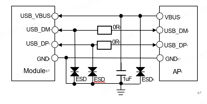
The data exchange between the host processor (AP) and the module is mainly completed through the USB interface. The USB of the module only supports slave mode.
The USB bus is mainly used for data transmission, firmware upgrade, module program detection, and can be simulated as a serial port mode to send AT commands. ESD devices need to be added externally to the DM/DP data line of USB, and the load capacitance of the ESD device must be less than 3 pF. The differential impedance of differential data lines needs to be controlled within 90ohm ± 10%, wrap the ground up, down, left, and right, and do not intersect with other wiring. The USB connection circuit is shown in the following diagram.
USB application circuit
Firmware upgrade
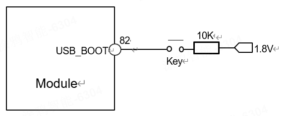
Module upgrade firmware can use a USB interface or serial port. If the module needs to upgrade firmware through the USB interface, it needs to enter USB download mode. When USB-BOOT (PIN82) is detected as high during module startup, it enters USB download mode. The recommended circuit for forced download is shown in the following figure.
Forced download pin recommendation circuit
If serial communication is used, a separate test point needs to be reserved for the USB_VBUS and USB_SM/DP signals of the module to facilitate software upgrades during debugging; If USB-DIM/DP is used to communicate with MCU, a test point needs to be reserved near the USB-DIM/DP signal of the module, and a 0R resistor needs to be connected in series on the USB-DIM/DP signal line. The resistor should be placed near the module, and the test point should be placed between the module and the resistor.
UART interface
Pin description
The L511-Y6 series module provides three serial communication interfaces UART: Among them, MAIN_UART serves as the fully functional serial asynchronous communication interface of the L511-Y6 series module, supporting signal control of standard modem handshake signals, complying with the RS-232 interface protocol, and also supporting 4-wire serial bus interface or 2-wire serial bus interface mode. The module can communicate with the outside world and input AT commands through the MAIN_UART interface. Modules can also upgrade firmware through the MAIN_UART interface. DBG_UART serves as the debugging serial port for L511-Y6 series modules and is a 2-wire UART interface. AUX_UART can be used to connect external devices.
These three sets of UART interfaces support programmable data width, programmable data stop bits, programmable parity bits, and independent TX and RX FIFOs. MAIN_UART supports baud rates of 600bps, 1200bps, 2400bps, 4800bps, 9600bps, 19200bps, 38400bps, 57600bps, 115200bps, 230400bps, 460800bps, and 921600bps. The default baud rate is 115200bps, which is used for data transmission and AT command transmission. DBG_UART supports a baud rate of 3Mbps and is used for partial log output.
The definition of UART pin signals is shown in the following table.
| Pin | Signal name | I/O type | Function description |
|---|---|---|---|
| 17 | MAIN_RXD | DI | Main UART receive data input |
| 18 | MAIN_TXD | DO | Main UART transmit data output |
| 19 | MAIN_DTR | DI | Main UART data terminal ready (wake up module) |
| 20 | MAIN_RI | DO | Main UART ring indicator |
| 21 | MAIN_DCD | DO | Main UART data carrier detect |
| 22 | MAIN_CTS | DO | Main UART clear to send |
| 23 | MAIN_RTS | DI | Main UART request to send |
| 28 | AUX_RXD | DI | Auxiliary UART receive data input |
| 29 | AUX_TXD | DO | Auxiliary UART transmit data output |
| 38 | DBG_RXD | DI | Debug UART receive data input |
| 39 | DBG_TXD | DO | Debug UART transmit data output |
UART interface application
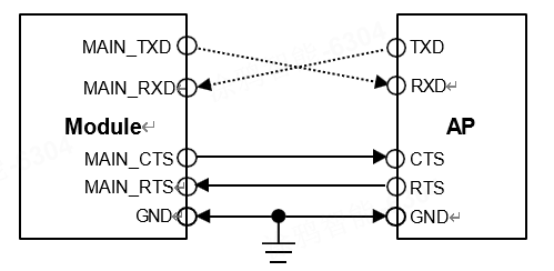
If the MAIN_UART is used for communication between the module and the application processor, and the voltage level matches at 1.8V, the connection method is shown as follows. It can be connected in full RS232 mode, 4-wire mode, or 2-wire mode.
Module serial port and AP application processor 4-wire connection method
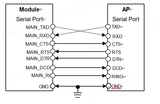
Complete connection between module serial port and AP application processor
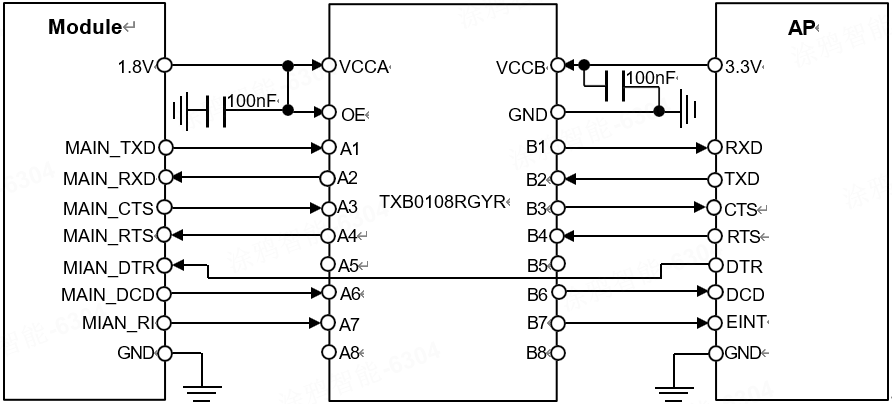
Due to the serial voltage domain of the module being 1.8V, if the voltage domain of the customer’s application system is 3.3V, a level translation chip needs to be added to the serial connection between the module and the customer’s application system. It is recommended to use Texas Instruments’ level translation chip.
Level translation reference circuit
MAIN_DTR can be directly connected to the GPIO port of the MCU ranging from 1.8V to 3.3V. MAIN_DTR suggests reserving 20K pull-up resistors to 1.8V-3.3V. MAIN_RXD suggests adding a 10K pull-up resistor to 1.8V. When the module serial port matches the AP terminal level, it is recommended to add a 10K pull-up resistor to 1.8V for MAIN_TXD.
Status indication interface
Network indicator light control circuit
The module has a NET_STATUS network status pin. The reference circuit is shown in the following figure.
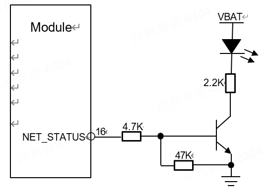
Network indicator pin status description
The logic level changes of NET_STATUS (PIN16) under different network states are shown in the following table.
The working status of the network status indicator pin
| LED status | Module status |
|---|---|
| Turn off | Power off |
| 64ms on/800ms off | Shut down network |
| 64ms on/3000ms off | Registered network |
Interactive application interface
Pin description
The interfaces shown in the table mainly interact with the application processor, including two types of interfaces: wake-up (wake-up includes wake-up modules and module wake-up peripherals) and status query.
| Pin | Signal name | I/O type | Function description |
|---|---|---|---|
| 19 | MAIN_DTR | DI | Input signal of AP wake-up module |
| 20 | MAIN_RI | DO | Module wakes up the output signal of the AP |
| 25 | STATUS | DO | AP query module boot status |
Interface application
The L511-Y6 series modules provide direct interaction signals for communication with application processors.
- MAIN_DTR: After the module enters sleep mode, the host can wake up the module by setting the signal low. After the host is set to high level, the module is allowed to enter sleep mode. MAIN_DTR can be directly connected to the GPIO port of MCU ranging from 1.8V to 3.3V.
- MAIN_RI: When a module has an event that requires communication with the application processor, the module can output a low level (which lasts for 120ms) through this pin to wake up the application processor.
- Status: Module status query, low level indicates shutdown or startup initialization state, high level indicates startup state.
ADC interface
The module provides two ADCs for detecting photoresistors or other devices that require ADC detection. The ADC supports 12 bit precision and has a maximum value of 1.2V. The ADC characteristics are shown in the table below.
| Characteristics | Minimum value | Typical value | Maximum value | Unit |
|---|---|---|---|---|
| Input voltage range | 0.05 | - | 1.2 | V |
Electrical characteristics and reliability
Electrical characteristics
| Parameter | Minimum value | Recommended Value | Maximum value | Unit |
|---|---|---|---|---|
| VBAT | 3.3 | 3.8 | 4.5 | V |
| Peak current | - | - | 1.2 | A |
Low voltage may cause the module to fail to start up properly; Excessive voltage or power on overshoot may also cause permanent damage to the module.
Temperature characteristics
| Status | Minimum value | Room temperature value | Maximum value | Unit |
|---|---|---|---|---|
| Working temperature | -40 | +25 | +85 | °C |
| Storage temperature | -45 | +25 | +90 | °C |
When the working temperature exceeds the working temperature of the module, some RF performance of the module may deteriorate, and it may also cause faults such as shutdown and restart.
Absolute maximum rated parameter
Absolute maximum rated parameters of power supply
| Pin Name | Description | Minimum value | Typical value | Maximum value | Unit |
|---|---|---|---|---|---|
| VDD_EXT | Digital power for IO | -0.3 | 1.8 | 1.98 | V |
| RESET_N | System reset signal | -0.3 | - | 3.6 | V |
| VBAT | Power supply | -0.3 | - | 5 | V |
Recommended operating conditions
Recommended operating range for power supply
| Signal | Description | Minimum | Typical | Maximum | Unit |
|---|---|---|---|---|---|
| USB_VBUS | USB power detection | 4.5 | 5 | 5.5 | V |
| VDD_EXT | Digital power for IO | 1.7 5 | 1.8 | 1.85 | V |
Power consumption
| Category | Test scenario | Minimum | Average | Maximum | Unit |
|---|---|---|---|---|---|
| Power off mode | VBAT=3.8V | - | 1 | - | uA |
| Flight mode | VBAT=3.8V/AT+CFUN=0 AT+ECPMUCFG=1,1 |
- | 3.6 | - | mA |
| Sleep1 | VBAT=3.8V/AT+CFUN=0 AT+ECPMUCFG=1,2 |
- | 68 | - | uA |
| Sleep2 | VBAT=3.8V/AT+CFUN=0 AT+ECPMUCFG=1,3 |
- | 15 | - | uA |
| LTE Standby | VBAT=3.8V/AT+ECPMUCFG=1,2 | - | 0.98 | - | mA |
| Peak current | VBAT=3.8V | - | - | 1.2 | A |
The power consumption is measured by laboratory instruments.
Module part working mode
| Working mode | Description | Remarks |
|---|---|---|
| Flight mode | IDLE mode at CPU, VDD_EXT outputs normally | - |
| Sleep1 | VDD_EXT outputs normally, 16KB cache runs, 1MB SRAM runs | The module can be awakened through MAIN_DTR (requires sending AT+QSCLK=1 to pull up the interface for wake-up) |
| Sleep2 | VDD_EXT outputs normally, 16KB cache is running, 1MB SRAM is turned off | Same as Sleep1 |
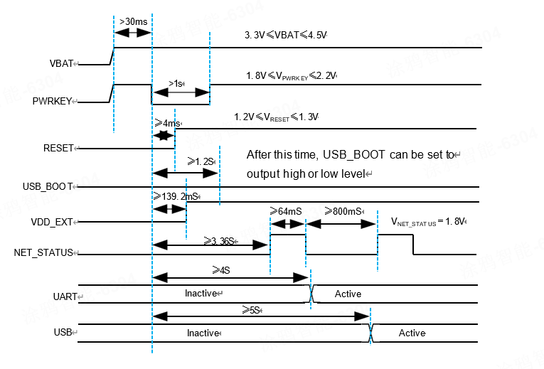
Power on timing
Digital interface characteristics
| Parameters | Description | Minimum value | Typical value | Maximum value | Unit |
|---|---|---|---|---|---|
| VIH | Input High Level | 0.7 * VDD_EXT | 1.8 | 1.85 | V |
| VIL | Input low level | 0 | - | 0.2 * VDD_EXT | V |
| VOH | Output High Level | 0.8 * VDD_EXT | 1.8 | 1.85 | V |
| VOL | Output low level | 0 | - | 0.15 * VDD_EXT | V |
Suitable for GPIO, UART and other interfaces.
Static protection
In module applications, static electricity may cause certain damage to the module, so static electricity protection must be taken into account during production, assembly, and operation of the module.
The ESD performance parameters (temperature: 25 °C, humidity: 45%) are shown in the following table.
| Pin | Contact discharge | Air discharge |
|---|---|---|
| VBAT | ±5 kV | ±10 kV |
| GND | ±5 kV | ±10 kV |
| ANT | ±5 kV | ±10 kV |
How to enhance ESD performance:
-
If the customer comes with an adapter board, the feet of the adapter board should be as many as possible and evenly distributed, with a wide ground conduction path.
-
ESD devices need to be added to the buttons (including the power button, forced download button, and reset button); Do not place the reset button wire near the edge of the board.
-
UART and other patch cords require ESD devices, and control lines pulled out from outside the module also require ESD devices.
-
ESD devices also need to be added to the areas that users will touch when inserting and removing (U) SIM cards.
-
Please add ESD devices to the external antenna, with a load capacitance of less than 0.1pF.
- To ensure ESD performance, please strengthen ESD performance according to the above measures.
- ESD devices can use varistors and TVS tubes. If higher performance requirements are needed, please use TVS tubes.
- Pay attention to the selection of voltage range for ESD devices on the power supply.
Frequency function
Main characteristics of RF
- Supports FDD/TDD LTE Rel-14 C at.1bis
- Supports LTE frequency bands B1/B3/B5/B7/B8/B18/B19/B20/B26/B28/B34/B38/B39/B40/B41
The operating frequency range of the transmitter and receiver of this product is shown in the following table:
| Working frequency band | Uplink | Downlink |
|---|---|---|
| FDD Band1 | 1920 MHz to 1980 MHz | 2110 MHz to 2170 MHz |
| FDD Band3 | 1710 MHz to 1785 MHz | 1805 MHz to 1880 MHz |
| FDD Band5 | 824 MHz to 849 MHz | 869 MHz to 894 MHz |
| FDD Band7 | 2500 MHz to 2570 MHz | 2620 MHz to 2690 MHz |
| FDD Band8 | 880 MHz to 915 MHz | 925 MHz to 960 MHz |
| FDD Band18 | 815 MHz to 830 MHz | 860 MHz to 875 MHz |
| FDD Band19 | 830 MHz to 845 MHz | 875 MHz to 890 MHz |
| FDD Band20 | 832 MHz to 862 MHz | 791 MHz to 821 MHz |
| FDD Band26 | 814 MHz to 849 MHz | 859 MHz to 894 MHz |
| FDD Band28 | 703 MHz to 748 MHz | 758 MHz to 803 MHz |
| TDD Band34 | 2010 MHz to 2025 MHz | 2010 MHz to 2025 MHz |
| TDD Band38 | 2570 MHz to 2620 MHz | 2570 MHz to 2620 MHz |
| TDD Band39 | 1880 MHz to 1920 MHz | 1880 MHz to 1920 MHz |
| TDD Band40 | 2300 MHz to 2400 MHz | 2300 MHz to 2400 MHz |
| TDD Band41 | 2496 MHz to 2690 MHz | 2496 MHz to 2690 MHz |
Output power
| Frequency band | Maximum power | Minimum power |
|---|---|---|
| FDD Band1 | 23 dBm±2dB | < -40 dBm |
| FDD Band3 | 23 dBm±2dB | < -40 dBm |
| FDD Band5 | 23 dBm±2dB | < -40 dBm |
| FDD Band 7 | 23 dBm±2dB | < -40 dBm |
| FDD Band8 | 23 dBm±2dB | < -40 dBm |
| FDD Band18 | 23 dBm±2dB | < -40 dBm |
| FDD Band19 | 23 dBm±2dB | < -40 dBm |
| FDD Band20 | 23 dBm±2dB | < -40 dBm |
| FDD Band26 | 23 dBm±2dB | < -40 dBm |
| FDD Band28 | 23 dBm±2dB | < -40 dBm |
| TDD Band34 | 23 dBm±2dB | < -40 dBm |
| TDD Band38 | 23 dBm±2dB | < -40 dBm |
| TDD Band39 | 23 dBm±2dB | < -40 dBm |
| TDD Band40 | 23 dBm±2dB | < -40 dBm |
| TDD Band41 | 23 dBm±2dB | < -40 dBm |
Reception sensitivity
| Frequency band | REF SENS @ 10 MHz (Total) |
|---|---|
| FDD Band1 | ≤ -96.3 dBm |
| FDD Band3 | ≤ -93.3 dBm |
| FDD Band5 | ≤ -94.3 dBm |
| FDD Band7 | ≤ -94.3 dBm |
| FDD Band8 | ≤ -93.3 dBm |
| FDD Band18 | ≤ -96.3 dBm |
| FDD Band19 | ≤ -96.3 dBm |
| FDD Band20 | ≤ -93.3 dBm |
| FDD Band26 | ≤ -93.8 dBm |
| FDD Band28 | ≤-94.8 dBm |
| TDD Band34 | ≤ -96.3 dBm |
| TDD Band38 | ≤ -96.3 dBm |
| TDD Band39 | ≤ -96.3 dBm |
| TDD Band40 | ≤ -96.3 dBm |
| TDD Band41 | ≤ -94.3 dBm |
Antenna Circuit Design
The access part of the RF antenna of this product adopts the form of PAD pads. The module antenna pad and the customer motherboard antenna interface need to be connected through pad welding and microstrip or strip lines. The microstrip line or strip line is designed with a characteristic impedance of 50 ohms, and the routing length is less than 10mm, while reserving a π - shaped matching circuit.
When designing the peripheral circuit of the product antenna, it is recommended to follow the layout scheme of the RF circuit: the RF line should be routed on the first layer, referring to the ground plane on the second layer.
When designing PCB wiring, it is important to note that the RF path needs to be fully referenced to the ground plane.
Antenna matching network:
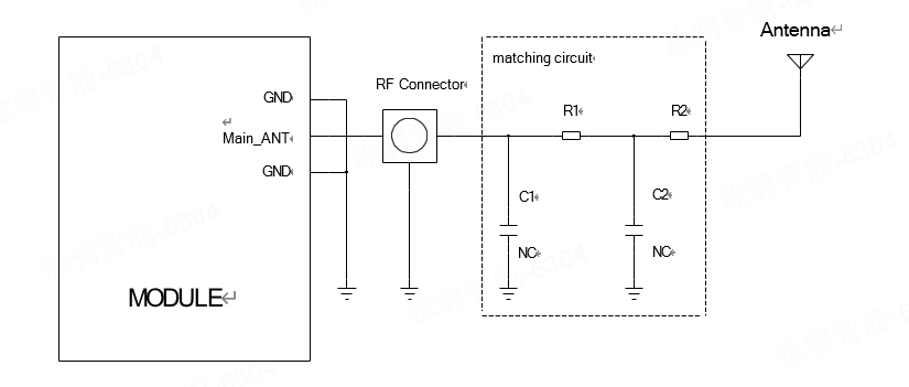
- In the figure, R1, C1, C2, and R2 form an antenna matching network for antenna debugging. By default, R1 and R2 are labeled with 0-ohm resistors, while C1 and C2 are labeled empty. The values will be determined after the antenna factory has debugged the antenna.
- The RF connector in the figure is reserved for conducting tests (such as CE certification, FCC certification, etc.) and should be placed as close to the module as possible. The RF path from the module pad to the antenna feed point should maintain a 50-ohm impedance control.
In Layout design, the RF transmission line of the antenna must ensure a characteristic impedance of 50 ohms, which is determined by the substrate board, routing width, and distance from the ground plane. The following figure shows the reference design of the antenna path in Layout.
Antenna path reference design

Antenna design
It is recommended to use PIFA or IFA antennas for internal antennas, and whip antennas for external antennas. The recommended antenna gain is around 3dBi. Suggested built-in antenna area: 100mm * 10mm * 6mm (length * width * height), PCBA length greater than 90mm. Avoid the Speaker, Motor, MIC, Camera FPC, and Camera Body within 5cm around the antenna LCD FPC, switching power supplies, high-speed signal lines, memory, CPUs, and other components and modules that are prone to EMI.
antenna parameters
| Antenna parameters | Parameter requirements |
|---|---|
| Antenna efficiency | >40% |
| S11/VSWR | <-10dB |
| Polarization mode | linear polarization |
| TRP Low Band | >18 dBm |
| TRP Middle Band | >18 dBm |
| TRP High Band | >18 dBm |
| TIS Low Band | <- 92 dBm (@10 MHz) |
| TIS Middle Band | <- 92 dBm (@10 MHz) |
| TIS High Band | <- 92 dBm (@10 MHz) |
| Low Band | Band 5/8/18/19/20/26/28 |
| Middle Band | Band 1/3/34/39 |
| High Band | Band 7/38/40/41 |
Storage, production, and packaging
Material storage
The moisture resistance level of the module is level three, and there are obvious humidity-sensitive warning messages on the labels of the outer packaging box and inner packaging bag of the finished product.
When the original vacuum packaging is intact (without damage or air leakage), the storage period is 12 months, and the storage environment requires a temperature below 40°C, humidity below 90%, and good air circulation.
The following table lists the shelf life of modules corresponding to different levels of humidity sensitivity.
| Level | Factory environment 23 ± 5°C, relative humidity < 60% RH |
|---|---|
| 1 | No control < 30°C/85% RH |
| 2 | One year |
| 2a | 4 weeks |
| 3 | 168 hours |
| 4 | 72 hours |
| 5 | 48 hours |
| 5a | 24 hours |
| 6 | Before use, it must be baked and passed through the oven within the time specified on the label |
The handling, storage, and processing of modular products must comply with the requirements of IPC/JEDEC J-STD-033.
Production of SMT
SMT modules are humidity-sensitive devices. If reflow soldering production and subsequent disassembly and maintenance are required, strict adherence to humidity-sensitive device requirements must be followed in the storage, production, and maintenance processes of finished products.
If the module is subjected to reflow soldering or repaired with a hot air gun after being dampened, it can cause the IC or PCB inside the module to burst due to the rapid expansion of water vapor, resulting in physical damage to the components and other defects. Typical faults include bubbling on the PCB board, and failure of BGA devices and RF modules due to bursting. So, customers should refer to the following suggestions when using the module.
Module incoming material confirmation and moisture prevention
The module is strictly operated according to the humidity-sensitive device process during production and packaging. The factory packaging includes vacuum bags, desiccants, and humidity indicator cards, with strict humidity control. Customers are requested to pay attention to moisture control before applying the patch, and to confirm the following steps for incoming materials.
Confirmation of baking requirements
The modules are uniformly shipped in vacuum packaging and can be stored for 12 months without damage to the packaging. The environmental temperature requirement is below 40 °C and the relative humidity is less than 90%. If one of the following conditions is met, sufficient baking should be carried out before reflow soldering, otherwise, the module may cause permanent damage during the reflow soldering process:
- Storage time expired
- Check for packaging damage, vacuum packaging leakage, etc
- The humidity indicator card changes color at 10%
- The module is left exposed and stationary in the air for 168 hours or more
- The module is exposed to air for less than 168 hours and does not meet the environmental conditions of temperature<30 °C and relative humidity<60%
The moisture resistance level of the module is level three, and the baking conditions are as follows.
| Baking conditions | 125 ± 5 °C/5% RH | 45 ± 5 °C/5% RH |
|---|---|---|
| Baking time | 8 hours | 192 hours |
| Explanation | Original tray cannot be used | Original tray can be used |
- The temperature resistance of the original anti-static tray should not exceed 50 °C, otherwise, the tray will deform.
- The original anti-static tray is only used for packaging purposes and cannot be used as a patch tray.
- During the process of taking and placing, anti-static measures should be taken, and attention should be paid to not stacking.
Customer product repair
If the module is disassembled for furnace maintenance, damp modules are easily damaged during disassembly. Therefore, module disassembly and other related maintenance operations should be completed within 48 hours after SMT, otherwise the module needs to be baked before disassembly.
The repair and disassembly of customer-returned products from on-site engineering, as the modules cannot be guaranteed to be in a dry state, must be baked according to the baking conditions before disassembling and repairing the modules. If exposed to a humid environment for a long time, please extend the baking time appropriately, such as 125°C/36 hours.
Precautions for SMT reflow soldering
Due to the use of BGA chips, surface mount resistors, capacitors, and other surface mount materials inside the module, which are also connected to the PCB using solder, they will also melt at high temperatures. If the furnace temperature is too high when the module passes through the furnace, the solder inside the module will completely melt. If the module encounters significant vibrations, such as excessive vibration of the conveyor belt or collision with the board in the reflow soldering furnace, the BGA and other components inside the module are prone to displacement or false soldering. So, when using intelligent modules to pass through the furnace, attention should be paid to:
- The module should not generate significant vibration during furnace passing, and customers are required to pass through furnaces with tracks (chains) as much as possible, avoiding passing through wire mesh to ensure smooth passing.
- The maximum furnace temperature during actual production should not be too high. On the premise of meeting the welding quality of customer motherboards and module pads, the lower the furnace temperature, the shorter the duration of the maximum temperature, the better.
Some customers had inappropriate furnace temperature curves and high furnace temperatures when going online. The soldering situation of the customer’s motherboard was good, but the module defect rate caused by the furnace was high. After analysis, the reason was that the BGA chip was soldered again, resulting in device offset and short circuit. So please ask the customer to make necessary adjustments according to the actual conditions of their own factory.
Improvement suggestions for SMT steel mesh design and low tin false welding problem
During reflow soldering of modules, a small number of customers have experienced module false soldering or short circuit problems, mainly due to insufficient solder on module pads, PCB board warping and deformation, or excessive solder paste. It is recommended that customers verify and improve from the following aspects:
- It is recommended to use stepped steel mesh, and it is suggested that the thickness of the steel mesh in the module area be greater than that of the surrounding components. Please verify and adjust according to the actual thickness of the solder paste, as well as the actual conditions and experience of each company. The product needs to undergo strict processes such as trial production, capacity ramp-up, and mass production.
- Steel mesh mesh mesh method. Referring to the module packaging, users can make adjustments based on their respective company experience values. The steel mesh outside the solder pads around the module expands outward.
Precautions for SMT surface mount welding
If the customer’s motherboard is thin or thin, there is a risk of deformation, warping, etc. during the soldering process, which may lead to virtual soldering, insufficient soldering, etc. It is recommended to make a "soldering carrier" to ensure the welding quality. Other production suggestions are as follows:
- The solder paste adopts active solder paste from brands such as Alpha.
-Modules must be mounted using SMT machines (important), and manual placement or soldering is not recommended. - To ensure the quality of the patch, please confirm the necessary process conditions according to the actual situation of the patch factory before normal mass production, such as The pressure and speed of SMT (very important), as well as the drilling method of the steel mesh.
- Reflow soldering furnaces with a temperature range of 8 or higher must be used, and the furnace temperature curve must be strictly controlled.
Furnace temperature suggestion:
- B. Constant temperature zone: temperature 140-210 °C, time: 60s -20s
- E. Reflux zone: PEAK temperature 220-2 45 °C, time: 45s-75s
Furnace temperature curve
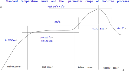
- The deformation of the customer’s bottom plate after passing through the furnace must be well controlled; Deformation can be reduced by reducing the number of patches or increasing the number of surface mount fixtures.
- It is recommended to increase the thickness of the steel mesh in the module, while maintaining a thickness of 0.1mm in other areas.
Packaging information
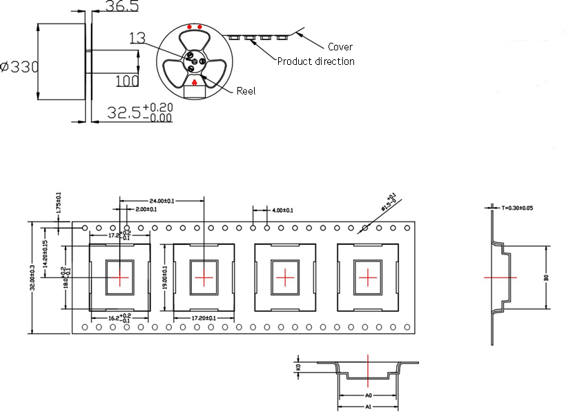
The L511-Y6 series modules are packaged with roll tape and sealed with vacuum-sealed anti-static bags.
Roll material tape
One roll material strip contains 500 modules, and the specific roll material strip information (unit: mm) is shown in the following figure.
Is this page helpful?
YesFeedbackIs this page helpful?
YesFeedback


