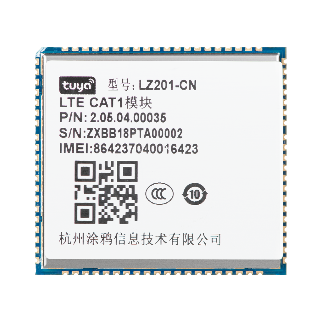
LZ201-CN Module Datasheet
LZ201-CN is an LTE Cat.1 cellular network module that Tuya has developed. Embedded with the LTE CAT.1 network communication protocol stack and rich library functions, it consists of a highly integrated LTE Cat.1 chip (UIS8910DM) and a few peripheral circuits.
Product overview
LZ201-CN has the Cortex A5 processor and Cat.1bis modem inside and is integrated with the 64-MB Nor flash memory and 128-MB PSRAM. It supports interfaces including USB, UART, SDIO, SPI, I2C, I2S and ADC. Besides, it also supports peripherals, such as display, camera, keyboard matrix, microphone, speaker, charging, MicroSD card and USIM card.
Features
- Cortex A5 processor and the clock rate of CPU: 500 MHz
- Supply voltage:
- Working voltage: 3.4 to 4.3 V
- Typical working voltage: 3.8 V
- SIM card: 1.8V/3V
- Features of LTE Cat.1:
- Frequency band
- LTE-FDD: B1/B3/B5/B8
- LTE-TDD: B34/38/39/40/41 (2535 to 2655 MHz)
- Data rate
- LTE-FDD: Max 10 Mbit/s (downlink)/Max 5 Mbit/s (uplink)
- LTE-TDD: Max 8.2 Mbit/s (downlink)/Max 3.4 Mbit/s (uplink)
- Transmit power: 23 ± 2 dBm
- Receiving sensitivity: Less than -98 dBm
- Antenna impedance 50Ω, an external antenna required
- Frequency band
- Bluetooth LE 4.2
- Wi-Fi SCAN
- Interfaces:
- 1 USB 2.0
- 3 UARTs
- 2 I2Cs
- 1 PCM/I2S
- 1 SDIO
- 1 SPI
- 3 ADC
- Peripherals:
- SPI display with the resolution of QVGA 320x240 and 30 FPS
- SPI/MIPI camera with 300,000 pixels
- 4*5 matrix keyboard
- 1 microphone
- 1 speaker
- MicroSD card
- Charging
- Normal working temperature: -30°C to +75℃ 1
- Extended working temperature: -40°C to +85℃ 2
- Support to upgrade firmware with the OTA technology
Note:
1 indicates that when the module is in the working temperature range, the performance related to the module meets the 3GPP standard.
2 indicates that when the module is in the working temperature range, the module can still work normally, but some RF indicators might exceed the standard values in the 3GPP slightly.
Applications
- Public utilities: Meter reading (water, gas and electricity), intelligent water affairs (pipe network, leakage and quality inspection), smart fire extinguisher, fire hydrant, etc.
- Smart health: Drug traceability, remote medical monitoring, blood pressure meter, blood glucose meter, heart armour monitoring, baby monitor, etc.
- Smart city: Smart street lights, smart parking, urban trash can management, public safety alarms, urban environment monitoring (water pollution, noise, air quality PM2.5, etc.)
- Consumers: Wearable devices, bicycles, mopeds anti-theft, smart luggage, VIP tracking (children, elderly, pets and vehicle rental), and payment/POS machines
- Agricultural environment: Precision planting (environment parameters: water, temperature, sunshine, biocide and fertilizer), animal husbandry (health and tracking), aquaculture and food safety traceability
- Logistics warehousing: Asset, container tracking, warehouse management, fleet management tracking, and logistics status tracking.
- Smart building: Access control, smart HVAC, smoke detection, fire detection and elevator failure/repair
- Manufacturing industry: Production, equipment status monitoring, energy facilities, oil and gas monitoring, chemical park monitoring, large-scale rental equipment and predictive maintenance (home appliances, machinery, etc.)
Module interfaces
Pin distribution
LZ201-CN has 144 pins in total. Among them, there are 80 LCC-packaged pins and 64 LGA-packaged pins.
The diagram of correspondence between pin ID and pin name
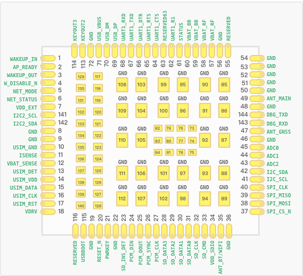
Pin definition
| Pin number | Pin name | Signal type | Description |
|---|---|---|---|
| 1 | WAKEUP_IN | I | Wakeup pin, used by the external device to wake up the module. Not connected to anything when it is not used. In OpenCPU mode, it can be used as GPIO 10. |
| 2 | AP_READY* | I | Used to detect the status of the processor. Not connected to anything when it is not used. In OpenCPU mode, it can be used as GPIO 11. |
| 3 | WAKEUP_OUT* | O | Wakeup pin, used by the module to wake up the external device. Not connected to anything when it is not used. In OpenCPU mode, it can be used as GPIO 5. |
| 4 | W_DISABLE_N* | I | Flight mode. Not connected to anything when it is not used. In OpenCPU mode, it can be used as GPIO 8. |
| 5 | NET_MODE | PI | Used to indicate the network registration status. Flashing fast indicates "in the progress of searching for the network". Flashing slowly indicates "already connected to the Tuya Cloud". |
| 6 | NET_STATUS* | O | Used to indicate the network running status. In OpenCPU mode, it can be used as GPIO 9. |
| 7 | VDD_EXT | PO | 1.8V. Offer the high level to the external GPIO. Not connected when it is not used. |
| 8 | GND | - | Ground. |
| 9 | GND | - | Ground. |
| 10 | USIM_GND | - | Ground. |
| 11 | ISENSE | I | Used to detect the current for charging. |
| 12 | VBAT_SENSE | I | Used to detect the voltage of the battery. Try to be as close to the positive electrode of the battery as possible. If the VBAT pin is not connected, the low-voltage shutdown function must be turned off, otherwise, the module will automatically shut down. |
| 13 | USIM_DET | I | Used to detect the hot swap of the USIM card. Not connected to anything when it is not used. |
| 14 | USIM_VDD | PO | Working voltage of the USIM card. The module automatically identifies the USIM card of 1.8 or 3.0V. |
| 15 | USIM_DATA | I/O | Data signal of the USIM card. |
| 16 | USIM_CLK | O | Clock signal of the USIM card. |
| 17 | USIM_RST | O | Reset signal of the USIM card. |
| 18 | VDRV | O | Enable the charging circuit. |
| 19 | GND | - | Ground. |
| 20 | RESET_N | I | Reset signal, low active. |
| 21 | PWRKEY | I | Power on or off. |
| 22 | GND | - | Ground. |
| 23 | SD_INS_DET | I | Used to detect the SD card. In OpenCPU mode, it can be used as GPIO 7. |
| 24 | PCM_DIN | I | Used to input PCM voice data. In OpenCPU mode, it can be used as GPIO 2. |
| 25 | PCM_DOUT | O | Used to output PCM voice data. In OpenCPU mode, it can be used as GPIO 3. |
| 26 | PCM_SYNC | I/O | Signal to synchronize PCM voices. In OpenCPU mode, it can be used as GPIO 1. |
| 27 | PCM_CLK | I/O | Clock signal of PCM voices. In OpenCPU, it can be used as GPIO 0. |
| 28 | SD_DATA3 | I | Data 3 of the SD card. Reuse the Wi-Fi SDIO. |
| 29 | SD_DATA2 | I | Data 2 of the SD card. Reuse the Wi-Fi SDIO. |
| 30 | SD_DATA1 | I | Data 1 of the SD card. Reuse the Wi-Fi SDIO. |
| 31 | SD_DATA0 | I | Data 0 of the SD card. Reuse the Wi-Fi SDIO. |
| 32 | SD_CLK | O | Clock signal of the SD card. Reuse the Wi-Fi SDIO. |
| 33 | SD_CMD | I/O | Command of the SD card. Reuse the Wi-Fi SDIO. |
| 34 | VDD_SDIO | PO | Power supply of the SD card. Reuse the Wi-Fi SDIO. |
| 35 | ANT_BT/WIFI | AI/O | Bluetooth and Wi-Fi antenna. |
| 36 | GND | - | Ground. |
| 37 | SPI_CS_N | I | SPI chip selection. |
| 38 | SPI_MOSI | I | SPI MOSI. |
| 39 | SPI_MISO | O | SPI MISO. |
| 40 | SPI_CLK | O | Clock signal of the SPI. |
| 41 | I2C_SCL | OD | Clock signal of the I2C. In OpenCPU mode, it can be used as GPIO 14. |
| 42 | I2C_SDA | OD | Data signal of the I2C. In OpenCPU mode, it can be used as GPIO 15. |
| 43 | ADC2 | AI | Interface 2 for analog-to-digital conversion. |
| 44 | ADC1 | AI | Interface 1 for analog-to-digital conversion. |
| 45 | ADC0 | AI | Interface 0 for analog-to-digital conversion. |
| 46 | GND | - | Ground. |
| 47 | ANT_GNSS | AI | GNSS antenna, which is not supported by LZ201-CN but supported by LZ211-CN. |
| 48 | GND | - | Ground. |
| 49 | ANT_MAIN | AI/O | Main antenna interface. |
| 50~54 | GND | - | Ground. |
| 55 | RESERVED | - | Reserved. |
| 56 | GND | - | Ground. |
| 57 | VBAT_RF | P | Power supply for the module RF. The voltage ranges from 3.4 to 4.3V. The nominal voltage is 3.8V and the current is 2 A. |
| 58 | VBAT_RF | P | Power supply for the module RF. The voltage ranges from 3.4 to 4.3V. The nominal voltage is 3.8V and the current is 2 A. |
| 59 | VBAT_BB | P | Power supply for the baseband. The voltage ranges from 3.4 to 4.3V. The nominal voltage is 3.8V and the current is 1 A. |
| 60 | VBAT_BB | P | Power supply for the baseband. The voltage ranges from 3.4 to 4.3V. The nominal voltage is 3.8V and the current is 1 A. |
| 61 | STATUS* | O | Module status output. In OpenCPU mode, it can be used as GPIO 23. |
| 62 | UART1_RI | O | Output of ring. In OpenCPU mode, it can be used as GPIO 12. |
| 63 | RESERVED63 | O | Reserved. |
| 64 | UART1_CTS | O | UART1-clean to send. In OpenCPU mode, it can be used as GPIO 18. |
| 65 | UART1_RTS | I | UART1-request to send. In OpenCPU mode, it can be used as GPIO 19. |
| 66 | UART1_DTR | I | UART1-data terminal ready. It’s the sleep control pin. |
| 67 | UART1_TXD | O | UART1-transmit data. Support the MCU connection. |
| 68 | UART1_RXD | I | UART1-receive data. Support the MCU connection. |
| 69 | USB_DP | I/O | USB differential data plus. It supports module burning and calibration. |
| 70 | USB_DM | I/O | USB differential data minus. It supports module burning and calibration. |
| 71 | USB_VBUS | PI | Pin for plug-in detection. |
| 72 | GND | - | Ground. |
| 73 | SPK_P | O | Speaker (+). |
| 74 | SPK_N | O | Speaker (-). |
| 75 | MIC_P | I | Microphone (+). |
| 76 | GND | - | Ground. |
| 77 | MIC_N | I | Microphone (-). |
| 78 | KEYIN1 | I/O | Key input 1. |
| 79 | KEYIN2 | I/O | Key input 2. |
| 80 | KEYIN3 | I/O | Key input 3. |
| 81 | KEYIN4 | I/O | Key input 4. |
| 82 | KEYIN5 | I/O | Key input 5. |
| 83 | KEYOUT0 | I/O | Key output 0. |
| 84 | KEYOUT1 | I/O | Key output 1. |
| 85 to 112 | GND | - | Ground. |
| 113 | KEYOUT2 | I/O | Key output 2. |
| 114 | KEYOUT3 | I/O | Key output 3. |
| 115 | USBBOOT | I/O | If you input 0 through the keyboard and pull the voltage to VDD_EXT before the module is powered on, the module will enter the USB download mode. |
| 116 | RESERVED116 | - | Reserved and not connected to anything. |
| 117 | CLK26M_OUT | O | The frequency of the output interface of the clock signal is 26 MHz. |
| 118 | RESERVED118 | - | Reserved and not connected to anything. |
| 119 | LCD_FMARK | O | SPI LCD frame alignment signal. |
| 120 | LCD_RSTB | O | SPI LCD reset signal. |
| 121 | LCD_SEL | O | SPI LCD selection. |
| 122 | LCD_CS | O | SPI LCD chip select. |
| 123 | LCD_CLK | O | SPI LCD clock signal. |
| 124 | LCD_SDC | O | SPI LCD selection of data command. |
| 125 | LCD_SIO | O | SPI LCD serial input/output. |
| 126 | VDDLCD | P | External LCD power supply |
| 127 | PM_ENABLE | O | Enable the external power supply LDO. In OpenCPU mode, it can be used as GPIO 13. |
| 128 | VDDCAMA | P | Camera VCAMA power supply. |
| 129 | CAM_PWDN | I/O | Camera CAM_PWDN signal. |
| 130 | CAM_SI1 | I/O | Camera CAM_SI1 signal. |
| 131 | CAM_SI0 | I/O | Camera CAM_SI0 signal. |
| 132 | CAM_RSTL | I/O | Camera CAM_RSTL signal. |
| 133 | CAM_REFCLK | O | Camera CAM_REFCLK signal. |
| 134 | CAM_SCK | I/O | Camera CAM_SCK signal. |
| 135 | UART2_RXD/WAKE_WLAN | O | The serial interface 2 receives data and supports module burning and calibration. It is also used by the external Wi-Fi module to wake up LZ201*. In OpenCPU mode, it can be used as GPIO 20. |
| 136 | UART2_TXD/WLAN_EN | O | The serial interface 2 transmits data and supports module burning and calibration. It is used by the external Wi-Fi module to enable *. In OpenCPU mode, it can be used as GPIO 21. |
| 137 | UART3_RXD/KEYOUT4 | I | The serial interface 3 receives data and reuses KEYOUT4. |
| 138 | UART3_TXD/KEYOUT5 | O | The serial interface 3 transmits data and reuses KEYOUT5. |
| 139 | ZSP_UART_TXD/BT_EN | O | The pin is used to output ZSP logs and also used by the external Bluetooth LE mesh module to enable *. In OpenCPU mode, it can be used as GPIO 22. |
| 140 | VDDCAMD | P | Camera VCAMD power supply. |
| 141 | I2C2_SCL | I/O | I2C clock signal. |
| 142 | I2C2_SDA | I/O | I2C data signal In OpenCPU mode, it can be used as GPIO 17. |
| 143 | DBG_TXD | I | The pin is used for debugging and transmitting data. |
| 144 | DBG_RXD | O | The pin is used for debugging and receiving data. |
Note: P indicates a power supply pin and I/O indicates an input/output pin. "*" indicates that the function is not supported currently.
Electrical parameters
Absolute electrical parameters
| Parameter | Description | Minimum value | Maximum value | Unit |
|---|---|---|---|---|
| Ts | Storage temperature | -40 | 90 | ℃ |
| VBAT | Supply voltage | -0.3 | 4.6 | V |
ESD features
| Location | Air charge | Contact charge |
|---|---|---|
| GND | ±10 KV | ±5 KV |
| Antenna interface | ±8 KV | ±4 KV |
| Other interfaces | ±1 KV | ±0.5 KV |
Normal working conditions
| Parameter | Description | Minimum value | Typical value | Maximum value | Unit |
|---|---|---|---|---|---|
| Ta | Working temperature | -30 | - | 75 | ℃ |
| Ta | Extended working temperature | -40 | - | 85 | ℃ |
| VBAT | Working voltage | 3.4 | 3.8 | 4.3 | V |
Direct-current parameters
1.8 V Digital I/O
| Parameter | Description | Minimum value | Typical value | Maximum value | Unit |
|---|---|---|---|---|---|
| VIL | I/O low-level input | - | - | 0.3*VCC | V |
| VIH | I/O high-level input | 0.7*VCC | - | VCC | V |
| VOL | I/O low-level output | - | - | 0.2*VCC | V |
| VOH | I/O high-level output | 0.8*VCC | - | VCC | V |
Standby and transmission power consumption
| Working Mode | Condition | Average value | Peak value (Typical value) | Unit |
|---|---|---|---|---|
| Standby current | LTE-TDD | 5.2 | - | mA |
| Standby current | LTE-FDD | 3.4 | - | mA |
| Constantly transmit (23 dBm) | LTE-TDD | 300 | 600* | mA |
| Constantly transmit (23 dBm) | LTE-FDD | 550 | 600* | mA |
Note: The 600 mA current is generated when the VBAT is in parallel connected to the 1000 μA capacitor. If there is no large capacitor, the peak current will be above 1A. So please pay attention to the power input.
RF parameters
Basic RF features
| Parameter | Description |
|---|---|
| LTE-FDD frequency band | LTE-FDD: B1/B3/B5/B8 |
| LTE-TDD frequency band | LTE-TDD: B34/B38/B39/B40/B41 |
| Wireless standard | 3GPP R13 |
| LTE-FDD rate | LTE-FDD: Max 10 Mbps (downlink)/max 5 Mbps (uplink) |
| LTE-TDD rate | LTE-TDD: Max 8.2 Mbps (downlink)/max 3.4 Mbps (uplink) |
| Antenna | Characteristic impedance of 50 Ω |
TX performance
TX performance:
| Frequency band | Minimum value | Maximum value | Unit |
|---|---|---|---|
| LTE-FDD B1 | <-39 | 23±2 | dBm |
| LTE-FDD B3 | <-39 | 23±2 | dBm |
| LTE-FDD B5 | <-39 | 23±2 | dBm |
| LTE-FDD B8 | <-39 | 23±2 | dBm |
| LTE-TDD B34 | <-39 | 23±2 | dBm |
| LTE-TDD B38 | <-39 | 23±2 | dBm |
| LTE-TDD B39 | <-39 | 23±2 | dBm |
| LTE-TDD B40 | <-39 | 23±2 | dBm |
| LTE-FDD B41 | <-39 | 23±2 | dBm |
RX performance
Receiving sensitivity:
| Frequency band | Typical value | Unit |
|---|---|---|
| LTE-FDD B1 | -98.5 | dBm |
| LTE-FDD B3 | -98 | dBm |
| LTE-FDD B5 | -98 | dBm |
| LTE-FDD B8 | -98.5 | dBm |
| LTE-FDD B34 | -100 | dBm |
| LTE-FDD B38 | -98.5 | dBm |
| LTE-FDD B39 | -101 | dBm |
| LTE-FDD B40 | -98.5 | dBm |
| LTE-FDD B41 | -98.5 | dBm |
Antenna information
Antenna type
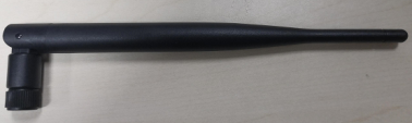
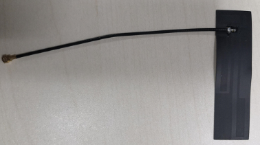
The module does not have its own onboard PCB antenna, and the third party needs to provide an antenna.
The antenna can be an external rod antenna, a spring antenna, an IPEX- FPC antenna, a PCB board antenna, etc. The antenna forms include monopole antenna, PIFA antenna, IFA antenna, loop antenna, etc.
-
Rod antenna
-
FPC antenna
Antenna design requirements
- Ensure that the characteristic impedance of the transmission line is 50Ω.
- Since the antenna line loss needs to be less than 0.3 dB, keep the PCB trace as short as possible.
- When designing the layout, you should choose the most direct and shortest route, to prevent routing through layers or holes, and rectangles and sharp angles.
- There is a good ground reference for the antenna, which stays away from other signal wires.
- It is recommended that you use the complete ground plane as the ground reference.
- Strengthen the connection between the ground around the antenna and the main ground.
- It is recommended that the antenna be at least 10 mm away from other metal parts.
Packaging information and production instructions
Mechanical dimensions
LZ201-CN has 144 pins in total. Among them, there are 80 LCC-packaged pins and 64 LGA-packaged pins.
The dimensions of LZ201-CN are 29±0.35 mm (W)×32±0.35 mm (L)×2.4±0.15 mm (H). The thickness of the PCB is 0.8±0.1 mm.
Mechanical dimensions and dimensions of the back of the pad
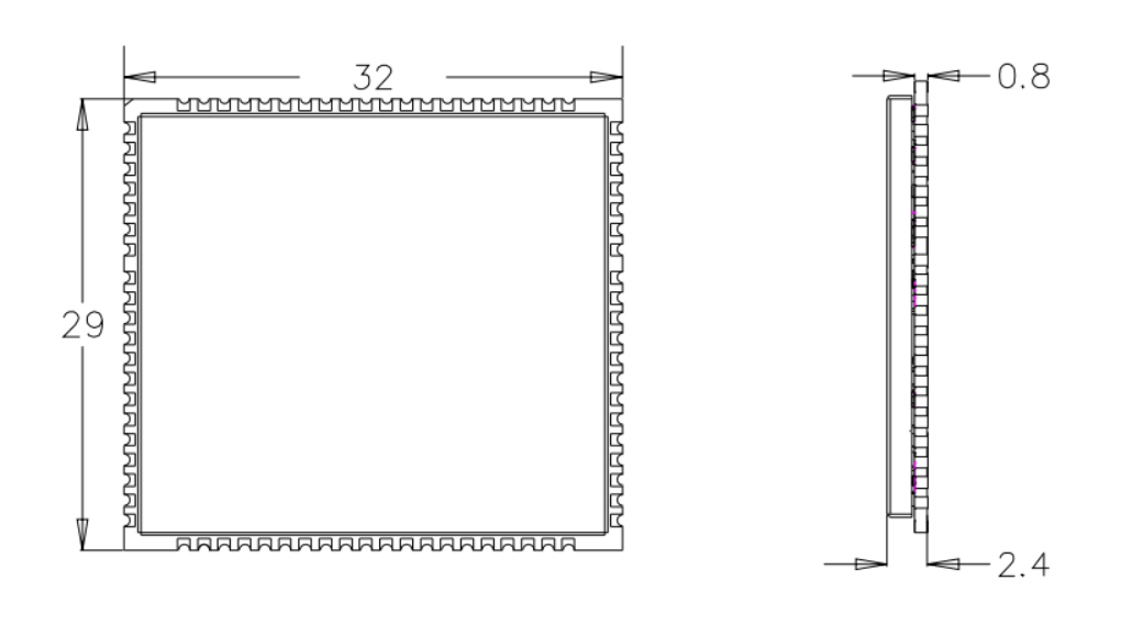
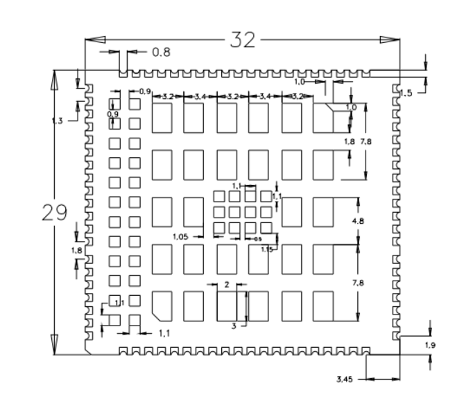
Note: The tolerance for the length and width of the module is ±0.35 mm, the height is ±0.15 mm, and the thickness is ±0.1 mm.
PCB packaging diagram-SMT
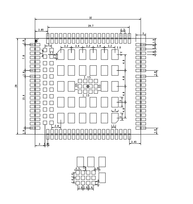
Top/bottom view of the module
Production instructions
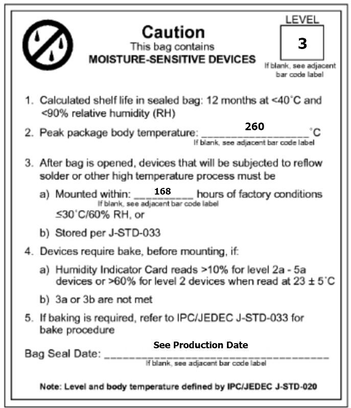
- The Tuya SMT module should be mounted by the SMT device. After being unpacked, it should be soldered within 24 hours. Otherwise, it should be put into the drying cupboard where the RH is not greater than 10%; or it needs to be packaged under vacuum again and the exposure time needs to be recorded (the total exposure time cannot exceed 168 hours).
- SMT devices:
- Mounter
- SPI
- Reflow soldering machine
- Thermal profiler
- Automated optical inspection (AOI) equipment
- Baking devices:
- Cabinet oven
- Anti-electrostatic and heat-resistant trays
- Anti-electrostatic and heat-resistant gloves
- SMT devices:
- Storage conditions for a delivered module:
-
The moisture-proof bag must be placed in an environment where the temperature is below 40°C and the relative humidity is lower than 90%.
-
The shelf life of a dry-packaged product is 12 months from the date when the product is packaged and sealed.
-
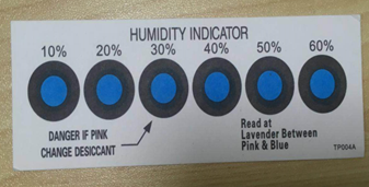
There is a humidity indicator card (HIC) in the packaging bag.
-
- The module needs to be baked in the following cases:
- The packaging bag is damaged before unpacking.
- There is no HIC in the packaging bag.
- After unpacking, circles of 10% and above on the HIC become pink.
- The total exposure time has lasted for over 168 hours since unpacking.
- More than 12 months have passed since the sealing of the bag.
- Baking settings:
- Temperature: 40°C and ≤ 5% RH for reel package and 125°C and ≤5% RH for tray package (please use the heat-resistant tray rather than plastic container)
- Time: 168 hours for reel package and 12 hours for tray package
- Alarm temperature: 50°C for reel package and 135°C for tray package
- Production-ready temperature after natural cooling: < 36°C
- Re-baking situation: If a module remains unused for over 168 hours after being baked, it needs to be baked again.
- If a batch of modules is not baked within 168 hours, do not use the reflow soldering to solder them. Because these modules are Level-3 moisture-sensitive devices, they are very likely to get damp when exposed beyond the allowable time. In this case, if they are soldered at high temperatures, it may result in device failure or poor soldering.
- In the whole production process, take electrostatic discharge (ESD) protective measures.
- To guarantee the passing rate, it is recommended that you use the SPI and AOI to monitor the quality of solder paste printing and mounting.
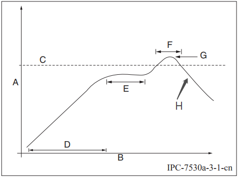
Recommended oven temperature curve
Set oven temperatures according to the following temperature curve of reflow soldering. The peak temperature is 245°C.
-
A: Temperature axis
-
B: Time axis
-
C: Liquidus temperature: 217 to 220°C
-
D: Ramp-up slope: 1 to 3°C/s
-
E: Duration of constant temperature: 60 to 120s; the range of constant temperature: 150 to 200°C
-
F: Duration above the liquidus: 50 to 70s
-
G: Peak temperature: 235 to 245°C
-
H: Ramp-down slope: 1 to 4°C/s
Note: The above curve is just an example of the solder paste SAC305. For more details about other solder pastes, please refer to Recommended oven temperature curve in the solder paste specifications.
Storage conditions
MOQ and packaging information
| Product number | MOQ (pcs) | Shipping packaging method | The number of modules per reel | The number of reels per carton |
|---|---|---|---|---|
| LZ201-CN | 2800 | Tape reel | 700 | 4 |
Is this page helpful?
YesFeedbackIs this page helpful?
YesFeedback


