LZ201-EAU Module Datasheet
LZ201-EAU is an LTE Cat.1 cellular module developed by Tuya Smart. The module consists of a highly integrated LTE Cat.1 chip UIS8910DM and peripheral circuits. It has a built-in LTE Cat.1 network communication protocol stack and library functions.
Overview
The LZ201-EAU module is built around an Arm Cortex-A5 processor and Cat.1 bis modem and embedded with a 64 MB NOR flash and a 128 MB PSRAM. It provides a wide array of interfaces including USB, UART, SDIO, SPI, I2C, I2S, and ADC for supporting peripherals such as the display, camera, keyboard matrix circuit, microphone, speaker, charger, microSD card, and USIM card.
Features
- Built-in Arm Cortex-A5 500 MHz application processor
- Supply voltage range:
- Operating voltage: 3.4V to 4.3V
- Typical operating voltage: 3.8V
- SIM card: 1.8V and 3V supported
- LTE Cat.1 features:
- Frequency bands
- LTE-FDD: bands 1, 3, 5, 7, 8, 20, and 28A*
- LTE-TDD: bands 38, 40, and 41
- GSM/GPRS: GSM900 and DCS1800
- Data transmission rate
- LTE-FDD: Maximum download speed of 10 Mbit/s, and maximum upload speed of 5 Mbit/s
- LTE-TDD: Maximum download speed of 8.2 Mbit/s, and maximum upload speed of 3.4 Mbit/s
- GSM/GPRS: Maximum download speed of 85.6 Kbit/s, and maximum upload speed of 42.8 Kbit/s
- Maximum transmit power: LTE: 23 ± 2 dBm, GSM: 33 ± 2 dBm, DCS: 30 ± 2 dBm
- Receiving sensitivity: LTE: less than -98 dBm, GSM: less than -108 dBm
- 50Ω antenna impedance, with an external antenna required
- Frequency bands
- Interfaces:
- 1 USB 2.0 interface
- 2 UART interfaces
- 2 I2C interfaces
- 1 PCM/I2C interface
- 1 SDIO interface
- 1 SPI interface
- 3 ADC interfaces
- 1 dedicated SPI flash interface
- Peripherals:
- SPI display, with a quarter VGA (QVGA) resolution of 320 × 240 pixels at 30 fps
- SPI/MIPI camera with a resolution of 640 × 480 pixels
- 4 × 5 keyboard matrix
- 1-channel microphone
- 1-channel speaker
- A microSD card
- Charging interface
- Operating temperature range: -30°C to +75°C 1
- Extended temperature range: -40°C to +85°C 2
- OTA firmware update
- B28A frequency range: TX 703 to 733 MHz; RX 758 to 788 MHz.
- 1 Within the operating temperature range, the module is 3GPP compliant.
- 2 Within the extended temperature range, the module still works properly. Only the values of one or more parameters like output power might exceed the specified tolerances of 3GPP specifications.
Scope of applications
- Smart health: medication tracker, remote patient monitoring, blood pressure monitor, blood glucose meter, health-tracking wearables, and baby monitor.
- Smart city: smart street lighting, smart parking, smart waste bin, public security alarm, and environment monitoring (water pollution, noise, air quality, PM2.5, and more).
- Consumer electronics: wearable, bicycle, GPS tracker (children, the elderly, pets, and car rental), smart suitcase, and POS machine.
- Agriculture and environment: precision planting (environmental parameters: water, temperature, light, medicine, fertilizer), livestock farming (health and tracking), aquaculture, and food quality monitoring.
- Logistics and warehousing: asset and container tracking, warehouse management, fleet tracking, and courier tracking.
- Smart buildings: access control, smart heating, ventilation, and air conditioning (HVAC), smoke detector, fire alarm, and elevator repair and maintenance.
- Manufacturing: equipment monitoring, energy monitoring, chemicals plants monitoring, large rental equipment, and predictive maintenance (home appliance and machinery).
- Public utilities: smart metering (water, gas, and electricity), smart water management (pipe network, leakage, and quality inspection), smart fire extinguisher, and smart fire hydrant.
Module interfaces
Pin definition
LZ201-EAU is equipped with a total of 144 pins, including 80 LCC pins and 64 LGA pins.
The pinout is as follows:
Pin definition
| Pin No. | Pin name | I/O type | Description |
|---|---|---|---|
| 1 | WAKEUP_IN | I | The external circuit wakes up the module. It can be used as GPIO10 in OpenCPU mode. If it is unused, keep it open. |
| 2 | AP_READY* | I | Used to inform the module whether the application processor is in sleep mode. It can be used as GPIO11 in OpenCPU mode. If it is unused, keep it open. |
| 3 | WAKEUP_OUT* | O | The module wakes up the external circuit. It can be used as GPIO5 in OpenCPU mode. If it is unused, keep it open. |
| 4 | W_DISABLE_N* | I | Used to force the module into airplane mode. It can be used as GPIO8 in OpenCPU mode. If it is unused, keep it open. |
| 5 | NET_MODE | PI | Indicate the module’s network registration mode, which applies when the module operates in self-processing mode. NET_MODE is a current source and connected to the LED GND pin. |
| 6 | NET_STATUS* | O | Indicate the module’s network activity status. It can be used as GPIO9 in OpenCPU mode. |
| 7 | VDD_EXT | PO | 1.8V voltage output. It can provide pull-up for the external circuit. If it is unused, keep it open. |
| 8 | GND | - | The ground pin. |
| 9 | GND | - | The ground pin. |
| 10 | USIM_GND | - | The ground pin. It shares the same network as GND. |
| 11 | ISENSE | I | Measure the charging current. |
| 12 | VBAT_SENSE | I | Measure the battery voltage. Connect it close to the positive terminal of batteries to sense the battery voltage. If the battery is not used, disable low voltage shutdown in the software. Otherwise, the module will shut down on low voltage. |
| 13 | USIM_DET | I | Detect the USIM card hot-plug, which is disabled by default in the software. Pull this pin up to VDD_EXT. |
| 14 | USIM_VDD | PO | Power supply for the USIM card. Either 1.8V or 3.0V is supported by the module automatically. |
| 15 | USIM_DATA | IO | USIM card data signal. |
| 16 | USIM_CLK | O | USIM card clock signal. |
| 17 | USIM_RST | O | USIM card reset signal. |
| 18 | VDRV | O | Enable the charger circuit. |
| 19 | GND | - | The ground pin. |
| 20 | RESET_N | I | Reset the module. Active low. |
| 21 | PWRKEY | I | Power on or off the system. Active low. |
| 22 | GND | - | The ground pin. |
| 23 | SD_INS_DET | I | Detect SD card insertion. It can be used as GPIO7 in OpenCPU mode. |
| 24 | PCM_DIN | I | PCM data input. It can be used as GPIO2 in OpenCPU mode. |
| 25 | PCM_DOUT | O | PCM data output. It can be used as GPIO3 in OpenCPU mode. |
| 26 | PCM_SYNC | IO | PCM data sync signal. It can be used as GPIO1 in OpenCPU mode. |
| 27 | PCM_CLK | IO | PCM audio clock signal. It can be used as GPIO0 in OpenCPU mode. |
| 28 | SD_DATA3 | I | SDIO data bit 3 of the SD card. It can be used as Wi-Fi SDIO. |
| 29 | SD_DATA2 | I | SDIO data bit 2 of the SD card. It can be used as Wi-Fi SDIO. |
| 30 | SD_DATA1 | I | SDIO data bit 1 of the SD card. It can be used as Wi-Fi SDIO. |
| 31 | SD_DATA0 | I | SDIO data bit 0 of the SD card. It can be used as Wi-Fi SDIO. |
| 32 | SD_CLK | O | SDIO clock signal of the SD card. It can be used as Wi-Fi SDIO. |
| 33 | SD_CMD | IO | SDIO command signal of the SD card. It can be used as Wi-Fi SDIO. |
| 34 | VDD_SDIO | PO | Power supply for the SD card. It can be used as Wi-Fi SDIO. |
| 35 | ANT_BT/WIFI | AIO | Bluetooth and Wi-Fi antenna. |
| 36 | GND | - | The ground pin. |
| 37 | SPI_CS_N | I | SPI chip select. |
| 38 | SPI_MOSI | I | SPI MOSI. |
| 39 | SPI_MISO | O | SPI MISO. |
| 40 | SPI_CLK | O | SPI clock signal. |
| 41 | I2C_SCL | OD | I2C clock signal. It can be used as GPIO14 in OpenCPU mode. |
| 42 | I2C_SDA | OD | I2C data signal. It can be used as GPIO15 in OpenCPU mode. |
| 43 | ADC2 | AI | Analog to digital converter interface 2. |
| 44 | ADC1 | AI | Analog to digital converter interface 1. |
| 45 | ADC0 | AI | Analog to digital converter interface 0. |
| 46 | GND | - | The ground pin. |
| 47 | ANT_GNSS | AI | GNSS antenna, supported by LZ211 and not supported by LZ201. |
| 48 | GND | - | The ground pin. |
| 49 | ANT_MAIN | AIO | Main antenna interface. |
| 50 to 54 | GND | - | The ground pin. |
| 55 | RESERVED | - | Reserved. |
| 56 | GND | - | The ground pin. |
| 57 | VBAT_RF | P | Power supply for module RF part. Supply voltage: 3.4V to 4.3V. Nominal voltage: 3.8V. Current: 2A. |
| 58 | VBAT_RF | P | Power supply for module RF part. Supply voltage: 3.4V to 4.3V. Nominal voltage: 3.8V. Current: 2A. |
| 59 | VBAT_BB | P | Power supply for baseband part. Supply voltage: 3.4V to 4.3V. Nominal voltage: 3.8V. Current: 1A. |
| 60 | VBAT_BB | P | Power supply for baseband part. Supply voltage: 3.4V to 4.3V. Nominal voltage: 3.8V. Current: 1A. |
| 61 | STATUS* | O | Internal use. |
| 62 | UART1_RI* | O | Ring indicator. It can be used as GPIO12 in OpenCPU mode. |
| 63 | RESERVED63 | O | Reserved. |
| 64 | UART1_CTS | O | UART 1 clear to send. It can be used as GPIO18 in OpenCPU mode. |
| 65 | UART1_RTS | I | UART 1 request to send. It can be used as GPIO19 in OpenCPU mode. |
| 66 | UART1_DTR* | I | Data terminal ready (DTR). |
| 67 | UART1_TXD | O | UART 1 transmit data. It can be connected to an external MCU. |
| 68 | UART1_RXD | I | UART 1 receive data. It can be connected to an external MCU. |
| 69 | USB_DP | IO | USB high-speed differential transceiver (positive). It can be used to download code to the module. |
| 70 | USB_DM | IO | USB high-speed differential transceiver (negative). It can be used to download code to the module. |
| 71 | USB_VBUS | PI | Detect USB insertion. |
| 72 | GND | - | The ground pin. |
| 73 | SPK_P | O | Speaker output signal (positive). |
| 74 | SPK_N | O | Speaker output signal (negative). |
| 75 | MIC_P | I | Microphone input signal (positive). |
| 76 | GND | - | The ground pin. |
| 77 | MIC_N | I | Microphone input signal (negative). |
| 78 | KEYIN1 | IO | Key input 1. |
| 79 | KEYIN2 | IO | Key input 2. |
| 80 | KEYIN3 | IO | Key input 3. |
| 81 | KEYIN4 | IO | Key input 4. |
| 82 | KEYIN5 | IO | Key input 5. |
| 83 | KEYOUT0 | IO | Key output 0. |
| 84 | KEYOUT1 | IO | Key output 1. |
| 85 to 112 | GND | - | The ground pin. |
| 113 | KEYOUT2 | IO | Key output 2. |
| 114 | KEYOUT3 | IO | Key output 3. |
| 115 | USBBOOT | IO | Key input 0. Pulling up this pin to VDD_EXT before power-on will force the module to enter USB download mode. |
| 116 | RESERVED116 | - | Reserved. Keep it open. |
| 117 | CLK26M_OUT* | O | 26M clock output signal. |
| 118 | RESERVED118 | - | Reserved. Keep it open. |
| 119 | LCD_FMARK | O | SPI LCD frame sync signal. |
| 120 | LCD_RSTB | O | SPI LCD reset signal. |
| 121 | LCD_SEL | O | SPI LCD selection. |
| 122 | LCD_CS | O | SPI LCD chip select. |
| 123 | LCD_CLK | O | SPI LCD clock signal. |
| 124 | LCD_SDC | O | SPI LCD data command selection. |
| 125 | LCD_SIO | O | SPI LCD data signal. |
| 126 | VDDLCD | P | External LCD power supply. |
| 127 | PM_ENABLE | O | External power LDO control. It can be used as GPIO13 in OpenCPU mode. |
| 128 | VDDCAMA | P | Power supply for camera VCAMA. |
| 129 | CAM_PWDN | IO | Camera CAM_PWDN signal. |
| 130 | CAM_SI1 | IO | Camera CAM_SI1 signal. |
| 131 | CAM_SI0 | IO | Camera CAM_SI0 signal. |
| 132 | CAM_RSTL | IO | Camera CAM_RSTL signal. |
| 133 | CAM_REFCLK | O | Camera CAM_REFCLK signal. |
| 134 | CAM_SCK | IO | Camera CAM_SCK signal. |
| 135 | UART2_RXD/WAKE_WLAN | O | UART 2 receive data. It can be used for the external Wi-Fi module to wake up the LZ201* module or used as GPIO20 in OpenCPU mode. Downloading code to the module is supported. |
| 136 | UART2_TXD/WLAN_EN | O | UART 2 transmit data. It can be used to enable the external Wi-Fi module* or used as GPIO21 in OpenCPU mode. Downloading code to the module is supported. |
| 137 | UART3_RXD/KEYOUT4 | I | UART 3 receive data. It can be used as KEYOUT4. |
| 138 | UART3_TXD/KEYOUT5 | O | UART 3 transmit data. It can be used as KEYOUT5. |
| 139 | ZSP_UART_TXD/BT_EN | O | ZSP log output. It can be used to enable the external Bluetooth Low Energy mesh module* or used as GPIO22 in OpenCPU mode. |
| 140 | VDDCAMD | P | Power supply for camera VCAMD. |
| 141 | I2C2_SCL | IO | I2C serial clock line. |
| 142 | I2C2_SDA | IO | I2C data signal. It can be used as GPIO17 in OpenCPU mode. |
| 143 | DBG_RXD | I | Debugging interface, used for the module to receive data. |
| 144 | DBG_TXD | O | Debugging interface, used for the module to transmit data. |
Pindicates the power pin.- I/O indicates the input and output pin.
*indicates this feature is not supported currently.
Electrical parameters
Absolute electrical parameters
| Parameter | Description | Min value | Max value | Unit |
|---|---|---|---|---|
| Ts | Storage temperature | -40 | 90 | °C |
| VBAT | Supply voltage | -0.3 | 4.6 | V |
ESD features
| Location | Air discharge | Contact discharge |
|---|---|---|
| GND | ±10 kV | ±5 kV |
| Antenna interface | ±8 kV | ±4 kV |
| Others | ±1 kV | ±0.5 kV |
Normal operating conditions
| Parameter | Description | Min value | Typical value | Max value | Unit |
|---|---|---|---|---|---|
| Ta | Operating temperature | -30 | - | 75 | °C |
| Ta | Extended operating temperature | -40 | - | 85 | °C |
| VBAT | Operating voltage | 3.4 | 3.8 | 4.3 | V |
Direct current parameters
1.8V digital I/O
| Parameter | Description | Min value | Typical value | Max value | Unit |
|---|---|---|---|---|---|
| VIL | I/O low-level input | - | - | 0.3 × VCC | V |
| VIH | I/O high-level input | 0.7 × VCC | - | VCC | V |
| VOL | I/O low-level output | - | - | 0.2 × VCC | V |
| VOH | I/O high-level output | 0.8 × VCC | - | VCC | V |
LTE/GSM power consumption
| Work mode | Condition | Average value | Peak (Typical) value | Unit |
|---|---|---|---|---|
| Standby current | LTE-TDD | 5.2 | - | mA |
| Standby current | LTE-FDD | 3.4 | - | mA |
| Continuous transmission (23 dBm) | LTE-TDD | 300 | 600* | mA |
| Continuous transmission (23 dBm) | LTE-FDD | 550 | 600* | mA |
| Continuous transmission (33 dBm) | GSM900 | 245 | 260* | mA |
| Continuous transmission (30 dBm) | DCS1800 | 180 | 200* | mA |
- The standby current is the minimum hardware current, excluding the TuyaOS application and heartbeat.
- The peak current is tested when VBAT is connected in parallel with a 1,000 μF capacitor. When there is no large capacitor, the peak current of the module reaches more than 1A. Pay attention to the power input.
RF parameters
Basic RF features
| Parameter | Description |
|---|---|
| LTE-FDD frequency band | LTE-FDD: bands 1, 3, 5, 7, 8, 20, and 28A |
| LTE-TDD frequency band | LTE-TDD: bands 38, 40, and 41 |
| GSM frequency band | GSM900 and DCS1800 |
| Wireless standard | 3GPP Release 13 |
| LTE-FDD speed | Maximum download speed of 10 Mbit/s and maximum upload speed of 5 Mbit/s |
| LTE-TDD speed | Maximum download speed of 8.2 Mbit/s and maximum upload speed of 3.4 Mbit/s |
| GSM/GPRS speed | Maximum download speed of 85.6 Kbit/s and maximum upload speed of 42.8 Kbit/s |
| Antenna type | 50Ω characteristic impedance |
Transmission performance
Continuous transmission performance
| Frequency bands | Min value | Max value | Unit |
|---|---|---|---|
| LTE-FDD B1 | < -39 | 23 ± 2 | dBm |
| LTE-FDD B3 | < -39 | 23 ± 2 | dBm |
| LTE-FDD B5 | < -39 | 23 ± 2 | dBm |
| LTE-FDD B7 | < -39 | 23 ± 2 | dBm |
| LTE-FDD B8 | < -39 | 23 ± 2 | dBm |
| LTE-FDD B20 | < -39 | 23 ± 2 | dBm |
| LTE-FDD B28A | < -39 | 23 ± 2 | dBm |
| LTE-TDD B38 | < -39 | 23 ± 2 | dBm |
| LTE-TDD B40 | < -39 | 23 ± 2 | dBm |
| LTE-FDD B41 | < -39 | 23 ± 2 | dBm |
| GSM900 | 5 ± 5 | 33 ± 2 | dBm |
| DCS1800 | 0 ± 5 | 30 ± 2 | dBm |
Receiving performance
Receiving sensitivity:
| Frequency bands | Typical value | Unit |
|---|---|---|
| LTE-FDD B1 | -98.5 | dBm |
| LTE-FDD B3 | -98.5 | dBm |
| LTE-FDD B5 | -98 | dBm |
| LTE-FDD B7 | -97.5 | dBm |
| LTE-FDD B8 | -98.5 | dBm |
| LTE-FDD B20 | -97.5 | dBm |
| LTE-FDD B28A | -97.5 | dBm |
| LTE-TDD B38 | -98.5 | dBm |
| LTE-TDD B40 | -98.5 | dBm |
| LTE-TDD B41 | -98.5 | dBm |
| GSM900 | -108 | dBm |
| DCS1800 | -108.5 | dBm |
Antenna information
Antenna type
This module does not come with an antenna, so an external antenna is required.
You can choose one from the external rubber antenna, helical antenna, FPC antenna with IPEX connector, and PCB antenna. The antenna type can be monopole, planar inverted‐F antenna (PIFA), inverted‐F antenna (IFA), loop, and more.
-
Rubber antenna:
-
FPC antenna:
Antenna design requirements
- Make sure the characteristic impedance of the transmission line is 50Ω.
- The antenna line loss should be less than 0.3 dB. Thus, keep the PCB trace as short as possible.
- The PCB layout should be as straight as possible to avoid vias and layer changes. Also, steer clear of right-angle and sharp-angle traces.
- A good reference ground should be set around the PCB traces, and other signal lines should be kept away from the antenna.
- A complete ground is recommended as a reference ground.
- The ground plane around the antenna must reinforce its connection to the main ground plane of the motherboard.
- The distance between the antenna and other mental components should be at least 10 mm.
Packing and production instructions
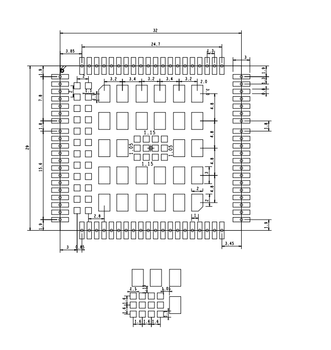
Mechanical dimensions
LZ201-EAU is equipped with a total of 144 pins, including 80 LCC pins and 64 LGA pins.
The dimensions are 29 ± 0.35 mm (W) × 32 ± 0.35 mm (L) × 2.4 ± 0.15 mm (H), as shown below. The PCB thickness is 0.8 mm ±0.1 mm.
Mechanical dimensions and backside pad dimensions
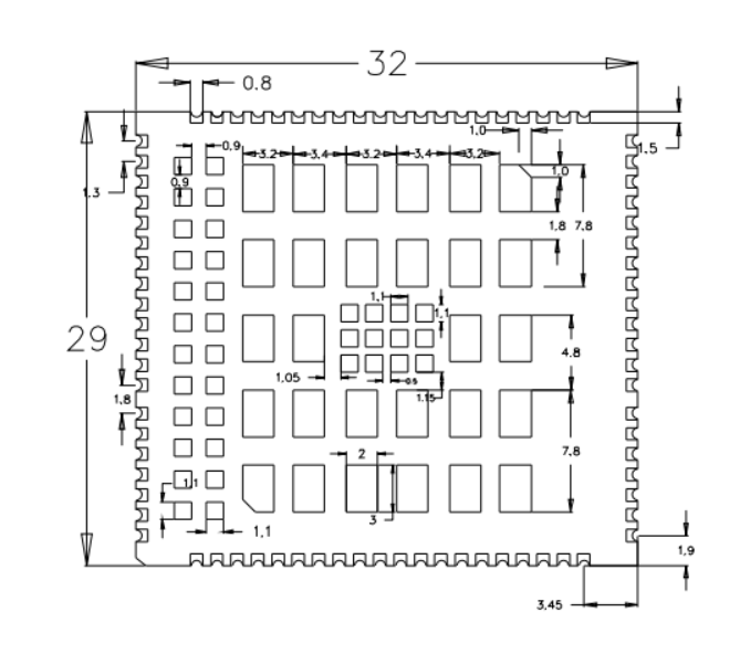
The tolerances for dimensions of length and width, height, and PCB thickness are ±0.35 mm, ±0.15 mm, and ±0.1 mm respectively.
SMT package
Stencil opening design
- Stencil thickness: The stencil thickness of the area for the module should be partly stepped up to 0.18 mm–0.2 mm. The stencil thickness in other positions is determined by product design.
- LCC pins: The stencil openings are shrunk inward by 0.1 mm, and moved outward by 1 mm along the direction of length. Along the width direction, the stencil openings are shrunk inward by 0.16 mm (each side by 0.08 mm) with a length of 1.4 mm (module’s pin length, avoiding solder beads), and are moved outward by 0.2 mm (each side by 0.1 mm) with a length of 2 mm (exposed on the areas outside of the bottom of the module pins to increase tinning).
- LGA pins: The total opening area of the stencil should be 60% of the pad. If it exceeds 60%, you can set a pitch of 0.3 mm.
Production instructions
-
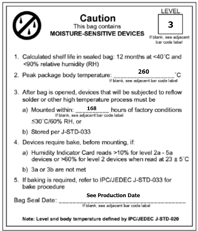
Package the module with the SMT if Tuya’s module is designed to be SMT-packaged. After being unpacked, the module must be soldered within 24 hours. Otherwise, it needs to be put into a drying cupboard with a relative humidity level no greater than 10%, or packed in vacuum again. Then, record the packing time and duration of exposure. The total exposure time cannot exceed 168 hours.
- Instruments or devices required for the SMT process:
- Surface mount system
- SPI
- Reflow soldering machine
- Thermal profiler
- AOI
- Instruments or devices required for the baking process:
- Cabinet oven
- Anti-electrostatic and heat-resistant trays
- Anti-electrostatic and heat-resistant gloves
- Instruments or devices required for the SMT process:
-
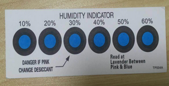
A delivered module must meet the following storage requirements:
-
The moisture-proof bag must be placed in an environment where the temperature is below 40°C and the relative humidity is lower than 90%.
-
The shelf life of a dry-packaged product is 12 months from the date when the product is packaged and sealed.
-
A humidity indicator card (HIC) is put in the sealed package.
-
-
The module needs to be baked in the following cases:
- The vacuum packaging bag is damaged before unpacking.
- After unpacking, no HIC is found in the packaging bag.
- After unpacking, the HIC indicates a humidity level of 10% or higher (the circle turns pink on the HIC).
- The total exposure time has lasted for over 168 hours since unpacking.
- More than 12 months have passed since the first sealing of the bag.
-
The baking parameter settings are described below:
- Baking temperature: 60°C for reel packaging with relative humidity ≤ 5%. And 125°C for tray packaging with relative humidity ≤ 5% (use the heat-resistant tray, rather than plastic containers).
- Baking time: 48 hours for reel packaging and 12 hours for tray packaging.
- Temperature for triggering an alert: 65°C for reel packaging and 135°C for tray packaging.
- Production can begin after a module has cooled down to below 36°C under natural conditions.
- If a module remains unused for over 168 hours after being baked, it needs to be baked again.
- If a batch of modules is not baked after exposure for more than 168 hours, do not use reflow soldering to solder them. Because these modules are level-3 moisture-sensitive devices, they are very likely to get damp when exposed beyond the allowable time. In this case, if they are soldered at high temperatures, device failure or poor soldering performance might occur.
-
In the whole production process, take electrostatic discharge (ESD) protective measures.
-
To guarantee the pass rate, we recommend that you use the SPI and AOI devices to monitor the quality of solder paste printing and mounting.
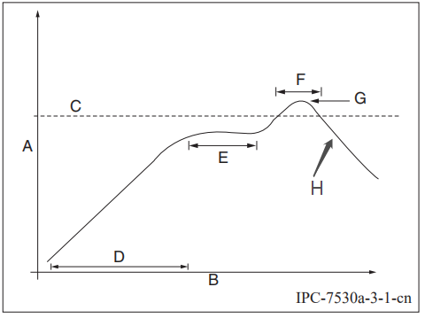
Recommended oven temperature curve
Perform the SMT process according to the following temperature curve of reflow soldering. The peak temperature is 245°C.
-
A: temperature axis
-
B: time axis
-
C: alloy liquidus temperature from 217°C to 220°C
-
D: ramp-up slope from 1°C/s to 3°C/s
-
E: keep a constant temperature from 150°C to 200°C for a time period from 60s to 120s
-
F: temperature above liquidus temperature for 50s to 70s
-
G: peak temperature from 235°C to 245°C
-
H: ramp-down slope from 1°C/s to 4°C/s
The curve above is based on solder paste SAC305. For more information about other solder pastes, see the recommended oven temperature curve in the specified solder paste specifications.
Storage conditions
MOQ and packaging information
| Product model | MOQ (pcs) | Shipping packaging | Modules per reel | Reels per carton |
|---|---|---|---|---|
| LZ201-EAU | 2,800 | Tape and reel | 700 | 4 |
Is this page helpful?
YesFeedbackIs this page helpful?
YesFeedback


