L511A Module Datasheet
Overview
The L511A/L511AN module is a Cat1 module for the LGA package, with stable and reliable performance. It can well meet customer’s requirements for cost-effective, low-power applications. It suits IoT areas, such as PoC, mobile payment, security and alarm systems, on-board vehicles, DTU, asset tracking, and sharing economy.
Hardware diagram
Main features
-
CPU
- ARM Cortex-M3@204MHz
-
Flash
- L511A/L511AN: >1MB SRAM+4MB Nor Flash
-
Frequency bands
-
FDD-LTE: B2/B4/B5/B12/B13/B66/B71
-
Output power
- LTE: 23dBm±2dB
-
Sensitivity
See table Receive sensitivity. -
Data transmission
- LTE-FDD: Max. DL 10Mbps, Max. UL 5Mbps
-
Power consumption
- LTE Standby: TBD mA @3.8V/AT+ECPMUCFG=1,2
-
Support Wi-Fi scan function
-
Built-in GNSS (L511AN supports GNSS function)
- Support GPS/GLONASS/Galileo/BeiDou
- GNSS shut down by default, open GNSS with AT command
- Receive channel: 47 channels
- Maximum update rate: 1Hz (Up to 10Hz)
- Tracking sensitivity: -165dBm
- Recapture sensitivity: -160dBm
- Cold start capture sensitivity: -148dBm
- Cold start TTFF: <25s
- Hot start TTFF: <1s
- Positioning accuracy: <2.5m CEP50
- Speed: <0.1m/s
Specifications
- Supply voltage range: 3.3 to 4.2V (typ3.8V)
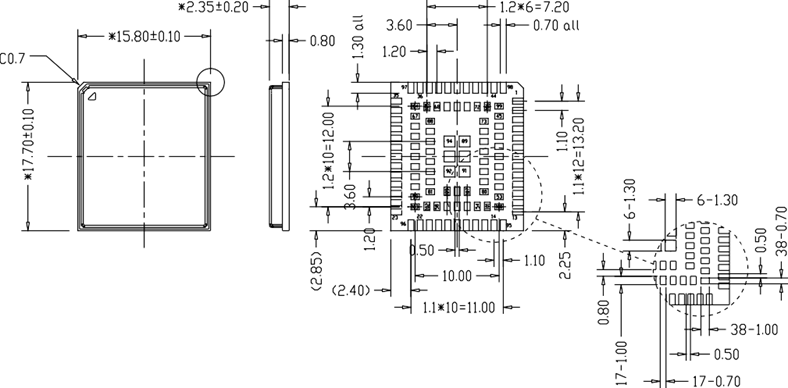
- Dimensions: 15.8mm * 17.7mm * 2.35mm
- 109-pin LGA
- Operation temperature range: -40°C to +85°C
- Storage temperature range: -45°C to +90°C
- Weight: about 1.3g
Interfaces
- GPIO
- USB2.0
- ADC
- PCM
- (U)SIM: Support 1.8V/3.0V
- UART
- Key
- Antenna
Peripherals features
- LCD: SPI interface 320*240
Module differences
| Module | AUX_RXD/AUX_TXD | GNSS |
|---|---|---|
| L511A | Yes | No |
| L511AN | No | Yes |
Package information
Pin configuration
Pin definition
The L511A/L511AN module has a total of 109 pins, and the specific functions of the interfaces are as follows.
| Pin NO. | Pin name | Type | Function description | Power domain | State(1) |
|---|---|---|---|---|---|
| LCC pin | |||||
| 1. | GND | G | Ground | - | GND |
| 2. | ANT_GNSS | ANT | GNSS antenna | - | Open |
| 3. | Reserved | - | Not connected | - | - |
| 4. | Reserved | - | Not connected | - | - |
| 5. | Reserved | - | Not connected | - | - |
| 6. | Reserved | - | Not connected | - | - |
| 7. | PWRKEY | DI | Power key button | 1.8 to 2.3V | Open |
| 8. | Reserved | - | Not connected | - | - |
| 9. | ADC0 | AI | ADC external input channel 0,12bit | 0.05 to 1.2V | Open |
| 10. | GND | G | Ground | - | GND |
| 11. | USIM1_DATA | DIO | USIM1 data | 1.8V/3.0V | Open |
| 12. | USIM1_RST | DO | USIM1 reset | 1.8V/3.0V | Open |
| 13. | USIM1_CLK | DO | USIM1 clock | 1.8V/3.0V | Open |
| 95. | GND | G | Ground | - | GND |
| 14. | USIM1_VDD | PO | USIM1 output voltage | 1.8V/3.0V | Open |
| 15. | RESET_N | DI | System reset signal | 1.25V | Open |
| 16. | NET_STATUS | DO | Output pin as LED control for network status | 1.8V | Open |
| 17. | MAIN_RXD | DI | Main UART receive data input | 1.45V | Open |
| 18. | MAIN_TXD | DO | Main UART transmit data output | 1.8V | Open |
| 19. | MAIN_DTR | DI | Main UART data terminal ready | 1.2V | Open |
| 20. | MAIN_RI | DO | Main UART ring indicator | 1.8V | Open |
| 21. | MAIN_DCD | DO | Main UART data carrier detect | 1.8V | Open |
| 22. | MAIN_CTS | DO | Main UART clear to send | 1.8V | Open |
| 96. | ADC1 | AI | ADC1 external input channel,12bit | 0.05 to 1.2V | Open |
| 23. | MAIN_RTS | DI | Main UART request to send | 1.8V | Open |
| 24. | VDD_EXT | PO | 1.8V output voltage, output current up to 2mA | 1.8V | Open |
| 25. | STATUS | DO | Output pin as operating status indicating of module | 1.8V | Open |
| 26. | I2S_MCLK | DO | I2S system clock | 1.8V | Open |
| 27. | GND | G | Ground | - | GND |
| 28. | AUX_RXD | DI | Auxiliary UART receive data input | 1.45V | Open |
| 29. | AUX_TXD | DO | Auxiliary UART transmit data output | 1.8V | Open |
| 30. | PCM_CLK | DO | PCM interface clock | 1.8V | Open |
| 31. | PCM_SYNC | DO | PCM interface sync | 1.8V | Open |
| 32. | PCM_DIN | DI | PCM I/F data in | 1.8V | Open |
| 33. | PCM_DOUT | DO | PCM I/F data out | 1.8V | Open |
| 34. | GND | G | Ground | - | GND |
| 35. | ANT_MAIN | ANT | Main Antenna | - | Open |
| 97. | Reserved | - | Not connected | - | - |
| 36. | GND | G | Ground | - | GND |
| 37. | GND | G | Ground | - | GND |
| 38. | DBG_RXD | DI | Debug UART receive data input | 1.45V | Open |
| 39. | DBG_TXD | DO | Debug UART transmit data output | 1.8V | Open |
| 40. | GND | G | Ground | - | GND |
| 41. | GND | G | Ground | - | GND |
| 42. | VBAT | PI | Power supply | 3.3 to 4.2V | VBAT |
| 43. | VBAT | PI | Power supply | 3.3 to 42V | VBAT |
| 44. | Reserved | - | Not connected | - | - |
| 98. | Reserved | - | Not connected | - | - |
| LGA PIN | |||||
| 45. | GND | G | Ground | - | GND |
| 46. | GND | G | Ground | - | GND |
| 47. | GND | G | Ground | - | GND |
| 48. | GND | G | Ground | - | GND |
| 49. | LCD_RST | DO | LCD reset signal | 1.8V | Open |
| 50. | LCD_SPI_OUT | DO | LCD SPI data out | 1.8V | Open |
| 51. | LCD_SPI_RS | DO | LCD SPI data /command selection | 1.8V | Open |
| 52. | LCD_SPI_CS | DO | LCD SPI chip-select | 1.8V | Open |
| 53. | LCD_SPI_CLK | DO | LCD SPI clock | 1.8V | Open |
| 54. | GPIO1 | I/O | General-purpose input/output | 1.8V | Open |
| 55. | GPIO2 | I/O | General-purpose input/output | 1.8V | Open |
| 56. | GPIO3 | I/O | General-purpose input/output | 1.8V | Open |
| 57. | GPIO4 | I/O | General-purpose input/output | 1.8V | Open |
| 58. | GPIO5 | I/O | General-purpose input/output | 1.8V | Open |
| 59. | USB_DP | IO | USB port differential data line | - | Open |
| 60. | USB_DM | IO | USB port differential data line | - | Open |
| 61. | Reserved | - | Not connected | - | - |
| 62. | USIM2_CLK | DO | USIM2 clock | 1.8V | Open |
| 63. | USIM2_RST | DO | USIM2 reset | 1.8V | Open |
| 64. | USIM2_DATA | DIO | USIM2 data | 1.8V | Open |
| 65. | USIM2_VDD | PO | USIM2 output voltage | 1.8V | Open |
| 66. | I2C_SDA | I/O | I2C data | 1.8V | Open |
| 67. | I2C_SCL | O | I2C clock | 1.8V | Open |
| 68. | Reserved | - | Not connected | - | - |
| 69. | Reserved | - | Not connected | - | - |
| 70. | GND | G | Ground | - | GND |
| 71. | GND | G | Ground | - | GND |
| 72. | GND | G | Ground | - | GND |
| 73. | GND | G | Ground | - | GND |
| 74. | Reserved | - | Not connected | - | - |
| 75. | Reserved | - | Not connected | - | - |
| 76. | Reserved | - | Not connected | - | - |
| 77. | Reserved | - | Not connected | - | - |
| 78. | LCD_TE | DO | LCD tearing effect | 1.8V | Open |
| 79. | USIM1_DET | DI | USIM1 detect pin | 1.2V | Open |
| 80. | Reserved | - | Not connected | - | - |
| 81. | Reserved | - | Not connected | - | - |
| 82. | USB_BOOT | DI | Force software download | 1.8V | Open |
| 83. | Reserved | - | Not connected | - | - |
| 84. | Reserved | - | Not connected | - | - |
| 85. | Reserved | - | Not connected | - | - |
| 86. | Reserved | - | Not connected | - | - |
| 87. | Reserved | - | Not connected | - | - |
| 88. | GND | G | Ground | - | GND |
| 89. | GND | G | Ground | - | GND |
| 90. | GND | G | Ground | - | GND |
| 91. | GND | G | Ground | - | GND |
| 92. | GND | G | Ground | - | GND |
| 93. | GND | G | Ground | - | GND |
| 94. | GND | G | Ground | - | GND |
| 99. | Reserved | - | Not connected | - | - |
| 100. | Reserved | - | Not connected | - | - |
| 101. | Reserved | - | Not connected | - | - |
| 102. | Reserved | - | Not connected | - | - |
| 103. | Reserved | - | Not connected | - | - |
| 104. | GRFC2 | DO | Generic RF Control 2 | 1.8V | Open |
| 105. | GRFC1 | DO | Generic RF Control 2 | 1.8V | Open |
| 106. | Reserved | - | Not connected | - | - |
| 107. | Reserved | - | Not connected | - | - |
| 108. | Reserved | - | Not connected | - | - |
| 109. | Reserved | - | Not connected | - | - |
(1) Suggested status when not in use.
- The PIN2 of L511A is reserved, and the L511AN supports GNSS function and PIN2 is ANT_GNSS.
- The PIN28 and PIN29 of L511A can be used to connect to external devices. The PIN28 and PIN29 of L511AN are reserved pins and cannot be connected to any external devices.
- The USB_BOOT (PIN82) pin must not be pulled up to high level before the module is successfully powered on.
- The VDD_EXT can output 1.8V during sleep; the voltage domain of the remaining 1.8V/1.45V interfaces will be turned off when the module is asleep, while the voltage domain of the 1.2V interfaces can function normally when the module is asleep.
- When the MAIN_RXD is enabled with the wake up function, the voltage domain of MAIN_RXD will change to 1.2V after the module is asleep.
| Pin type | Description |
|---|---|
| PI | Power input |
| PO | Power output |
| DI | Digital input |
| DO | Digital output |
| IO | Input output |
| AI | Analog input |
| ANT | Antenna |
| G | Ground |
Package information
Dimensions
The L511A module’s mechanical dimensions are described in the following figure (Top view, side view, and back view).
Product labeling
| Item | Description |
|---|---|
| A. | Pin1 mark |
| B. | Logo of company |
| C. | The finished part number of the module |
| D. | QR code—including IMEI number and SN number |
| E. | SN number |
| F. | IMEI number |
| G. | Module name |
| H. | Module configuration |
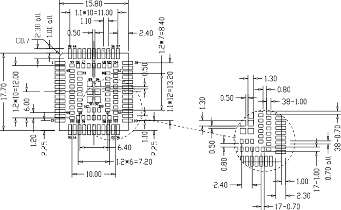
Module size
Recommended pad
Interface circuit design
Power section
Power supply
VBAT is the main power supply of the module, its voltage input range is 3.3V to 4.2V, and the recommended voltage is 3.8V. In poor network environments, where the antenna emits maximum power, the module must choose a power supply that can provide at least 1.2A current capability. A low ESR (ESR=0.7Ω) 100uF filter capacitor is recommended for the VBAT pin close to the module, and at the same time, it is recommended to add three (100nF, 33pF, 10pF) chip multilayer ceramic capacitors (MLCC) with the best ESR performance to VBAT respectively, and place the capacitors close to the VBAT pin. When connecting the module to an external power supply, VBAT requires star traces. The VBAT trace width should be no less than 1.2mm. In principle, the longer the VBAT trace, the wider the required trace width.
Considering various complex application scenarios of the module, it is strongly recommended that the module add TVS at VBAT to provide ESD/EOS protection for the module power supply. It is recommended to choose VRWM=4.7V and PPP≥500W for TVS.

When the module has no network, the RTC clock error of the module is relatively large, there will be a few minutes of error in 24 hours. If you want to get accurate time, you need to synchronize the network time.
If the voltage drop is not large, it is recommended to use LDO. LDO requires an over-current capacity of more than 1.2A, because LDO is a linear buck, its transient response capacity is poor, and the front and rear terminals need to be equipped with a large amount of capacitance, to prevent high-power transmission when the voltage fluctuation is too large, may lead to reset or shutdown. The output voltage needs to be controlled at 3.8V.
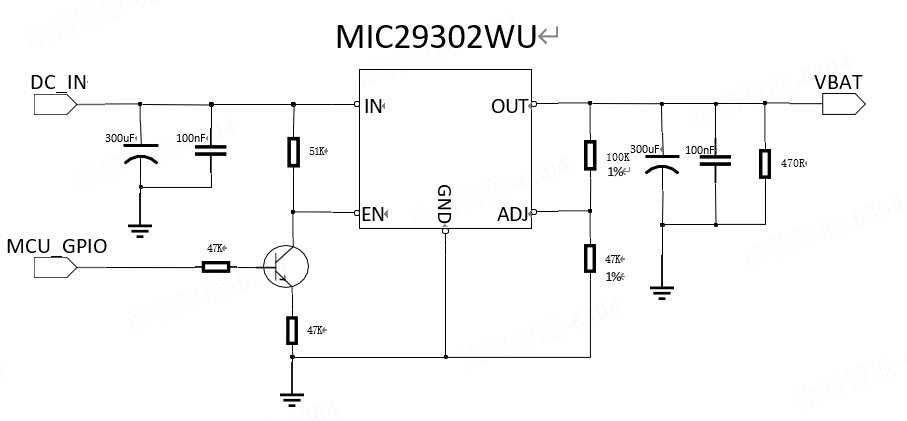
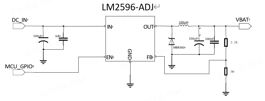
If the voltage drop is large, it is recommended to use DC/DC, the output current requirements of more than 1.2A, such as the following figure using a DC/DC switching power supply, supplemented by a large capacity (more than 330uF), to ensure the normal operation of RF PA (power amplifier). The advantage of the reference design is that it can provide a better transient current response, meet the working requirement of the module under the weak signal, and prevent the network drop or port restart caused by power shortage.
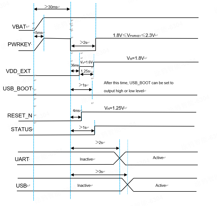
Hardware power on
Module 7-pin is the power-on key. Pulling down the PWRKEY at least 1s and then releasing, the module will boot. It is internally pull-up to 1.8V to 2.2V and does not need to pull up externally.
There are two ways to shut down the module:
- Use the AT command AT+POWEROFF to shut down the module and the shutdown process takes about 3s to complete.
- Pull down PWRKEY for more than 3s and then release to shut down.
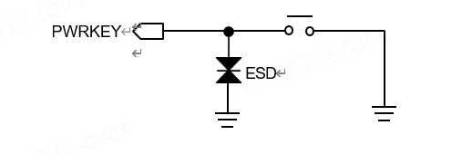
PWRKEY can be pulled down to the ground through a 0R resistor to achieve power-on and boot.
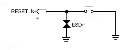
Hardware reset
Module 15-pin is the hardware reset input. The module will reset hardware when it receives a 1s low-level signal. It is internally pull-up to 1.25V and does not need to pull up externally. RESET_N can be directly connected to the 1.8V to 3.3V port of the MCU. The module will not restart after reset.
(U)SIM interface
Pin description
The L511A/L511AN module supports dual (U)SIM cards with a single standby. Module’s (U)SIM1 card (pin number: 11, 12, 13, 14) supports and can automatically detect 1.8V and 3.0V (U)SIM cards, (U)SIM2 card (pin number: 62, 63, 64, 65) only supports detecting 1.8V (U)SIM card.
The (U)SIM card interface signals are shown in the following table.
| Pin No. | Pin name | Signal description | Further description |
|---|---|---|---|
| 11 | USIM1_DATA | (U)SIM1 card data pin | (U)SIM1 card data signal, two-way signal |
| 12 | USIM1_RST | (U)SIM1 card reset pin | (U)SIM1 card reset signal, output by the module |
| 13 | USIM1_CLK | (U)SIM1 card clock pin | (U)SIM1 card clock signal, output by the module |
| 14 | USIM1_VDD | (U)SIM1 card power | (U)SIM1 card power supply, output by the module |
| 79 | USIM1_DET | (U)SIM1 card hot-plug detection pin | (U)SIM1 card hot plug detection signal, input signal |
| 62 | USIM2_CLK | (U)SIM2 card clock pin | (U)SIM2 card clock signal, output by the module |
| 63 | USIM2_RST | (U)SIM2 card reset pin | (U)SIM2 card reset signal, output by the module |
| 64 | USIM2_DATA | (U)SIM2 card data pin | (U)SIM2 card data signal, two-way signal |
| 65 | USIM2_VDD | (U)SIM2 card power | (U)SIM2 card power supply, output by the module |
(U)SIM interface application
The (U)SIM1 card signal group (pin numbers: 11, 12, 13, 14) and the (U)SIM2 card signal group (pin numbers: 62, 63, 64, 65), on the line near the (U)SIM card seat, please note the need to add ESD protection devices when designing.
In order to meet the requirements of 3GPP TS 27.005 protocol and EMC certification, the proposed (U)SIM card is arranged near the module (U)SIM card interface, and avoid layout too long resulting in serious waveform distortion, affecting the signal integrity. USIM_CLK and USIM_DATA signals are recommended to be protected. Paralleling a 1uF capacitor between GND and USIM_VDD, it can filter out the interference of radio frequency signals.
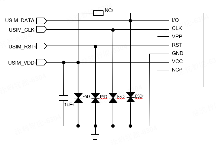
The ESD device capacitance is recommended to be less than 22pF. If you want to use the (U)SIM card hot swap function, you need to choose a (U)SIM card holder with a hot swap detection PIN.
USB interface
Pin description
The USB interface conforms to the USB 2.0 specification and electrical characteristics. It supports full-speed and high-speed modes. The data exchange between the main processor (AP) and the module is mainly completed through the USB interface. The module’s USB only supports slave mode.
The USB is mainly used for data transmission, firmware updates, module program testing, and sending AT commands. The USB_DM/DP differential impedance needs to be controlled at 90ohm ±10%, and it should be protected up and down, and cannot be crossed with other lines. The ESD device capacitance on USB_DM/DP is recommended to be less than 3pF. USB circuit is as follows.
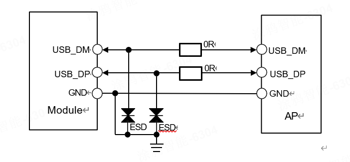
If you use the serial port communication, the USB_DM/DP reserved test points respectively to the firmware update. If USB_DM/DP is used to communicate with the MCU, the position of the USB_DM/DP signal near the module needs to reserve a test point and the USB_DM/DP requires a series 0R resistor. The resistor is placed near the module and the test point is placed between the module and the resistor.
Firmware upgrade
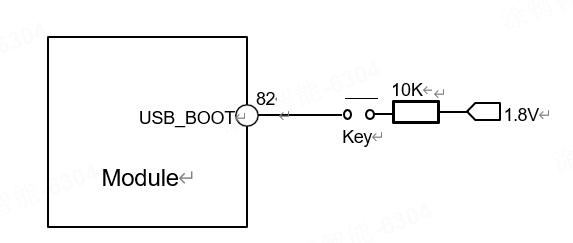
The L511A/L511AN module can use the USB interface or MAIN_UART interface to upgrade the firmware. The L511A module requires the module to enter the forced download mode when updating the firmware through the USB interface. When USB_BOOT (PIN82) is detected to be high level during module startup, the module enters USB download mode. The circuit of the USB_BOOT interface is as follows.
UART interface
Pin description
The L511A module provides three UART serial communication interfaces: MAIN_UART can be used as a complete non-synchronous communication interface, supporting standard modem handshake signal control and in compliance with the RS-232 interface protocol, also supporting 4-wire serial bus interface or 2-wire serial bus interface mode. DBG_UART is used as a debug port of the L511A module. The AUX_UART can be used to connect peripherals. The L511AN module only provides two UART serial communication interfaces, namely MAIN_UART and DBG_UART.
The three groups of UART ports support programmable data width, stop bits, and parity bits, with separate TX and RX FIFOs. The MAIN_UART supports 600bps, 1200bps, 2400bps, 4800bps, 9600bps, 19200bps, 38400bps, 57600bps, 115200bps, 230400bps, and 460800bps baud rates, and the default is 115200bps. This interface is used for AT command communication and data transmission. The DBG_UART supports a 3 Mbps baud rate for partial log output.
The pin signal definitions are shown in the following table.
| Pin No. | Pin name | I/O type | Functional description |
|---|---|---|---|
| 17 | MAIN_RXD | DI | Main UART receive data input |
| 18 | MAIN_TXD | DO | Main UART transmit data output |
| 19 | MAIN_DTR | DI | Main UART Data terminal ready (wake up module) |
| 20 | MAIN_RI | DO | Main UART ring indicator. |
| 21 | MAIN_DCD | DO | Main UART data carrier detect |
| 22 | MAIN_CTS | DO | Main UART clear to send |
| 23 | MAIN_RTS | DI | Main UART request to send |
| 28 | AUX_RXD | DI | Auxiliary UART receive data input |
| 29 | AUX_TXD | DO | Auxiliary UART transmit data output |
| 38 | DBG_RXD | DI | Debug UART receive data input |
| 39 | DBG_TXD | DO | Debug UART transmit data output |
UART interface application
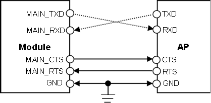
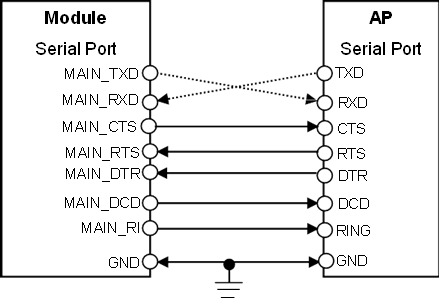
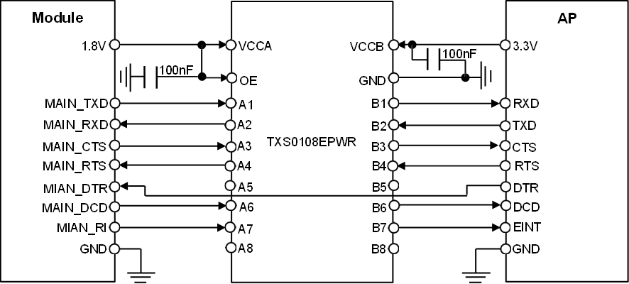
If using MAIN_UART in communication between the module and application processor, and the level is 1.8V, the connection mode is shown in the first two figures. You can use the complete RS232 mode, 4 wires, or 2 wires mode connection. The module interface level is 1.8V. If the AP interface level does not match, you must increase the level conversion circuit, as shown in the third figure.
MAIN_DTR can be directly connected to the 1.8V to 3.3V port of the MCU. MAIN_ DTR suggests reserving a 20K pull-up resistor to 1.8V to 3.3V. MAIN_RXD recommends adding a 10K resistor pull-up to 1.8V. When the UART of the module matches the AP level, MAIN_TXD recommends adding a 10K resistor pull-up to 1.8V.
Status indication interface
Network indicator control circuit
The module has a NET_STATUS pin. The reference circuit is shown in the following figure.

Network indication pin state
The logic level changes of NET_STATUS (PIN16) in different network states are shown in the table as follows.
| LED status | Module status |
|---|---|
| OFF | Power off |
| 64ms ON/800ms OFF | Shut down network |
| 64ms ON/3000 ms OFF | Registered network |
I2C interface
The L511A/L511AN module provides one group of I2C interfaces. This I2C can communicate with peripherals (such as sensors, codec, and so on) through the I2C interface.
| Pin NO. | Pin Name | Mode | Description |
|---|---|---|---|
| 66 | I2C_SDA | 100KHz/400KHz | Need to add a pull-up resistor to 1.8V externally, the resistor is recommended to use 4.7K |
| 67 | I2C_SCL |
Interactive application interface
Pin description
The L511A/L511AN module provides a variety of interfaces for interacting with the application processor, including WAKEUP (WAKEUP includes MAIN_DTR and MAIN_RI) and STATUS.
| Pin NO. | Pin name | I/O type | Function description |
|---|---|---|---|
| 19 | MAIN_DTR | DI | AP wakes up module |
| 20 | MAIN_RI | DO | Module wakes up AP |
| 25 | STATUS | DO | AP query module status |
Interface application
The L511A/L511AN module provides direct interactive signals to communicate with the AP.
MAIN_DTR: After the module enters sleep, the host can wake up the module by pulling down this signal. After the host pulls the signal high, the module is allowed to enter sleep.MAIN_DTRcan be directly connected to the 1.8V to 3.3V port of the MCU.MAIN_RI: When the module has an event and needs to communicate with the AP, the module can wake up the AP by setting this pin to a low level (Low level will last 120ms).STATUS: Module status query. A low level indicates the power-off state or power-on initialization state, and a high level indicates the power-on state.
LCD interface
The L511A/L511AN module supports the LCD function and only supports the SPI interface. It can provide a 3-wire/4-wire SPI interface for data transmission, and the supported resolution can reach 320*240. LCD_SPI_CLK can support up to 25.6 MHz. The interface modes of LCD are shown in the following table.
| Mode | LCD_CS | LCD_SPI_CLK | LCD_SPI_DOUT | LCD_SPI_RS |
|---|---|---|---|---|
| 3-wire 9bit mode | ● | ● | ● | / |
| 4-wire 8bit mode | ● | ● | ● | ● |
Digital audio interface
The L511A/L511AN module provides a digital audio interface (PCM) which can be used as the PCM master device to transmit digital voice signals. During use, the L511A/L511AN module is used as the master device to connect an external codec. PCM_SYNC and PCM_CLK are used as output pins.
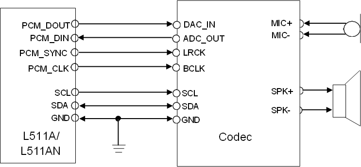
It is recommended to reserve an RC (R=22R, C=22pF) circuit on the signal line of PCM, especially on the PCM_CLK pin.
ADC interface
The module provides two ADC for detecting light-sensitive resistors or other devices that require ADC detection. The module supports 12-bit accuracy and the Max voltage of ADC is 1.2V.
| Characteristics | Min. | Typ. | Max. | Unit |
|---|---|---|---|---|
| Input voltage range | 0.05 | - | 1.2 | V |
Electrical features
Electricity
| Parameter | Min. | Nom. | Max. | Unit |
|---|---|---|---|---|
| VBAT | 3.3 | 3.8 | 4.2 | V |
| Peak current | - | - | 1.2 | A |
The over-low voltage cannot power on the module. Over-high voltage may be a danger to damage the module.
Temperature
| State | Min. | Nom. | Max. | Unit |
|---|---|---|---|---|
| Working | -40 | +25 | +85 | °C |
| Storage | -45 | +25 | +90 | °C |
When the temperature is over the range, the RF performance may be dropped. It also may cause power down or restart problems.
Absolute maximum power
| Pin name | Description | Min. | Typ. | Max. | Unit |
|---|---|---|---|---|---|
| VDD_EXT | Digital power for IO | -0.3 | 1.8 | 2 | V |
| RESET_N | System reset signal | -0.3 | - | 3.6 | V |
| VBAT | Power supply | -0.3 | - | 5 | V |
Recommended operating conditions
| Pin name | Description | Min. | Typ. | Max. | Unit |
|---|---|---|---|---|---|
| VDD_EXT | Digital power for IO | 1.75 | 1.8 | 1.85 | V |
Power consumption
| Parameter | Conditions | Min. | Average | Max. | Unit |
|---|---|---|---|---|---|
| Power off mode | VBAT=3.8V | - | 1 | - | uA |
| Flight mode | VBAT=3.8V/AT+CFUN=0, AT+ECPMUCFG=1,1 | - | 3.9 | - | mA |
| Sleep1 | VBAT=3.8V/AT+CFUN=0, AT+ECPMUCFG=1,2 | - | TBD | - | uA |
| Sleep2 | VBAT=3.8V/AT+CFUN=0, AT+ECPMUCFG=1,3 | - | TBD | - | uA |
| Hibernate | VBAT=3.8V/AT+CFUN=0, AT+ECPMUCFG=1,4 | - | TBD | - | uA |
| LTE standby | VBAT=3.8V/AT+ECPMUCFG=1,2 | - | TBD | - | mA |
| Peak current | VBAT=3.8V | - | 1.2 | - | A |
The test value of power consumption is the value tested in laboratory conditions.
| Operation mode | Description | Description |
|---|---|---|
| Flight mode | CPU is in IDLE mode, VDD_EXT output 1.8V | - |
| Sleep1 | VDD_EXT output 1.8V, 16KB cache operation, 1MB SRAM operation | It can be waked up by MAIN_DTR (need to send AT+QSCLK=1 to pull up the interface to wake up) |
| Sleep2 | VDD_EXT output 1.8V, 16KB cache operation, 1MB SRAM OFF | - |
Power sequence
Digital interfaces
| Parameter | Description | Min. | Typical | Max. | Unit |
|---|---|---|---|---|---|
| VIH | High-level input voltage | 0.7*VDD_EXT | 1.8 | 1.85 | V |
| VIL | Low-level input voltage | 0 | - | 0.2*VDD_EXT | V |
| VOH | High-level output voltage | 0.8*VDD_EXT | 1.8 | 1.85 | V |
| VOL | Low-level output voltage | 0 | - | 0.15*VDD_EXT | V |
Suit to all GPIO and UART interfaces.
ESD
The module contains highly sensitive electronics and is an electrostatic-sensitive device. More attention should be paid to the procedure of handling and packaging. The ESD test results are shown in the following table.
ESD parameter (Tem: 25°C, humidity: 45%)
| Pin name | Contact discharge | Air discharge |
|---|---|---|
| VBAT | ±5KV | ±10KV |
| GND | ±5KV | ±10KV |
| ANT | ±5KV | ±10KV |
Enhance ESD performance:
- If a converted board is added, it should have enough GND pins and be equally distributed. And the Layout of GND should be enough wide.
- Keys (Power key, USB_BOOT key, and RESET_N key) need to add ESD devices. The reset key line cannot be near the edge of the board.
- UART and other plug connectors need to add ESD devices, and the other control lines from the outside of the machine also need to add ESD devices.
- (U)SIM card should be added ESD protection.
- External antenna, please add ESD device, ESD Cpf<0.1pF.
For ESD protection, please add ESD methods according to the above-mentioned ways.
ESD components include varistors and TVS. For better performance, please use TVS. Pay attention to the selection of voltage range for ESD/TVS on the power supply.
RF features
RF main features
- Support FDD Cat1;
- Support LTE bands including band B2/B4/B5/B12/B13/B66/B71.
The operating frequency range of the product is shown in the table as follows.
| Band | Uplink band | Downlink band |
|---|---|---|
| FDD Band2 | 1850 MHz to 1910 MHz | 1930 MHz to 1990 MHz |
| FDD Band4 | 1710 MHz to 1755 MHz | 2110 MHz to 2155 MHz |
| FDD Band5 | 824 MHz to 849 MHz | 869 MHz to 894 MHz |
| FDD Band12 | 699 MHz to 716 MHz | 729 MHz to 746 MHz |
| FDD Band13 | 777 MHz to 787 MHz | 746 MHz to 756 MHz |
| FDD Band66 | 1710 MHz to 1780 MHz | 2110 MHz to 2180 MHz |
| FDD Band71 | 663 MHz to 698 MHz | 617 MHz to 652 MHz |
| Band | Maximum power | Minimum power |
|---|---|---|
| FDD Band2 | 23 dBm±2 dB | < -40 dBm |
| FDD Band4 | 23 dBm±2 dB | < -40 dBm |
| FDD Band5 | 23 dBm±2 dB | < -40 dBm |
| FDD Band12 | 23 dBm±2 dB | < -40 dBm |
| FDD Band13 | 23 dBm±2 dB | < -40 dBm |
| FDD Band66 | 23 dBm±2 dB | < -40 dBm |
| FDD Band71 | 23 dBm±2 dB | < -40 dBm |
| Band | REF SENS @10MHz (Total) |
|---|---|
| FDD Band 2 | ≤ -94.3 dBm |
| FDD Band 4 | ≤ -96.3 dBm |
| FDD Band 5 | ≤ -94.3 dBm |
| FDD Band 12 | ≤ -93.3 dBm |
| FDD Band 13 | ≤ -93.3 dBm |
| FDD Band 66 | ≤ -95.8 dBm |
| FDD Band 71 | ≤ -93.5 dBm |
Antenna circuit design
The connecting part of the RF antenna supports the PAD form. The connection between the module and the main board antenna interface is required to be welded and connected through a microstrip
line or a strip line. The microstrip line or strip line is designed according to the characteristic impedance of 50ohm, and the length of the wire is less than 10mm. Reserved ∏ matching network.
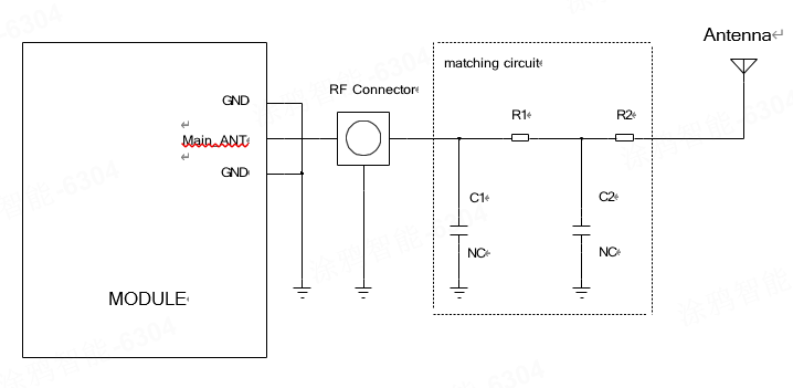
Figure R1, C1, C2, and R2 composition of the antenna matching network for antenna debugging, the default R1, R2 paste 0ohm resistor, and C2, C1 empty paste.
The RF connector in the figure is used for testing and conducting tests (for example, CE, FCC, etc.), which need to be placed as close as possible to the module, the RF path from the module to the antenna feed point should be kept under 50ohm impedance control.
This product antenna peripheral circuit design, the proposed RF circuit Layout program: RF line trances top layer, a reference to the second layer. Users need to pay attention to the design of the PCB line: to ensure the RF has a full reference GND layer.

Antenna design
PIFA or IFA antenna can be used for the inner antenna. Whip antenna can be used for an external antenna. The antenna gain must be more than 3dBi. The recommended area of the inner antenna: 100mm10mm6mm (LWH), the main board length is no less than 90mm. The antenna should be as far as possible from the chip and memory, power interface, data cable interface, camera FPC, screen FPC, connector FPC, and other possible EMI modules and devices.
| Antenna Parameters | Parameter Requirements | |
|---|---|---|
| Antenna efficiency | > 40% | |
| S11/VSWR | < -10dB | |
| Polarization mode | Linear polarization | |
| TRP | Low Band | > 18dBm |
| Middle Band | > 18dBm | |
| High Band | > 18dBm | |
| TIS | Low Band | < -92dBm (@10MHz) |
| Middle Band | < -92dBm (@10MHz) | |
| High Band | < -92dBm (@10MHz) | |
| Low Band | Band 5/12/13/71 | |
| Middle Band | Band 2/4/66 | |
GNSS
GNSS antenna selection and design
In order to obtain good GNSS reception performance, a good antenna needs to be selected. Proper antenna selection and placement ensure that satellite signals are received at all altitudes for fast and accurate positioning.
The GNSS built into the module has two antenna options:
- Passive antenna
- Active antenna
The recommended technical parameters of active and passive antennas are shown in the table as follows.
| Antenna type | Parameters | |
|---|---|---|
| Passive antenna | Frequency range | 1558-1607 MHz |
| Polarization | RHCP and linear | |
| Gain | > 0 dBi | |
| Active antenna | Frequency range | 1558-1607 MHz |
| Polarization | RHCP and linear | |
| Noise Figure | < 1.5 dB | |
| Gain | > 10 dBi | |
-
Passive antenna
Passive antennas are antennas with only radiating elements, such as ceramic antennas, helical antennas, and patch antennas. Passive antennas sometimes contain matching devices for 50ohm matching.
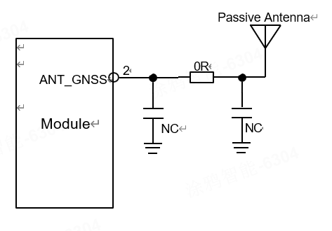
The most commonly used patch antenna in GNSS applications is the patch antenna, which is a planar structure, consisting of a ceramic body and a metal antenna body, and is mounted on a metal base plate.
The most simplified passive antenna design circuit of the GNSS antenna of the L511AN module is shown in the figure as follows.
-
Active antenna
Active antennas have an integrated low noise amplifier (LNA) and require an external power supply, which contributes to the power consumption of the GNSS system. The recommended circuit of an active antenna is shown in the figure as follows. Inductor L1 is to isolate the RF signal at the active antenna end into the power supply, and the recommended value is not less than 27nH. The role of R1 is to protect the entire circuit when the active antenna end is shorted to the ground.
Storage, production and package
Storage
The rank of moisture-proof of the module is level 3. There is an obvious sign on the table of the internal and the external packaging.
In the vacuum-sealed bag, the module can be stored for 12 months when the temperature is below 40°C and the humidity is below 90% under good air circulation.
The humidity level is described in detail as follows:
| Rank | Factory environment 23±5°C, relative humidity < 60%RH |
|---|---|
| 1 | No control < 30°C / 85%RH |
| 2 | One year |
| 2a | 4 weeks |
| 3 | 168 hours |
| 4 | 72 hours |
| 5 | 48 hours |
| 5a | 24 hours |
| 6 | Baking before using, SMT during the time table signs |
Moving, storage, and production of the module must meet the requirements of IPC/JEDEC J-STD-033.
Production
The module is a humidity-sensitive device. If the device needs reflow soldering, disassembly, and maintenance, we must strictly comply with the requirements of a humidity-sensitive device. If the module is damp, a reflow soldering or using hot-air gun maintenance will lead to internal damage, because the water vapor has the rapid expansion of the burst, causing physical injury to the device, like PCB foaming and BGA component failure. Refer to the following recommendations.
Confirmation and humidity
The module in the production and packaging process should be strictly in accordance with the humidity-sensitive device operation. The factory packaging is a vacuum bag, desiccant, and humidity indicator card. Please pay attention to the humidity control before SMT and the confirmation of the following aspects.
Baking
The smart module uses vacuum vacuum-sealed bag, which can make it stored for 12 months under the condition of temp 40°C and humidity < 90%. The module should be baked before reflowing soldering if any of the conditions below happen.
- Storage exceeds the time limit.
- Package damaged and vacuum bags have air leakage.
- Humidity indicating card change the color at 10%.
- Module is placed naked in the air over 168 hours.
- Module is placed naked in the air under 168 hours but not temp 30°C and humidity < 60%.
Baking condition
The moisture-proof level of the smart module is level 3. The baking conditions are as follows.
| Baking conditions | 125±5°C / 5%RH | 45±5°C / 5%RH |
|---|---|---|
| Baking time | 8 hours | 192 hours |
| Description | Not use the original tray | Can use the original tray |
The original anti-ESD tray temperature does not exceed 50°C. Otherwise, the tray will be deformed.
The anti-ESD tray of the original packaging is only used for packaging, and cannot be used as a SMT tray.
During taking and placing, take notes of ESD which cannot be placed as an overlay.
Customer product maintenance
For module maintenance after SMT, it is easy for a damp module to be damaged when removed, so the module disassembly and other related maintenance operations should be completed within 48 hours after SMT, or you need to bake and then maintain the module.
Because the module return from the fieldwork cannot ensure the dry state, it must be baked in accordance with the conditions of baking, then for disassembly and maintenance. If it has been exposed to a humid environment for a long time, please properly extend the baking time, such as 125°C/36 hours.
SMT reflow
The module has the BGA chips, chip resistances, and capacitances internally, which will melt at a high temperature. If the module melts completely due to a large shock, such as excessive vibration of the reflux conveyor belt or hits the board, internal components will easily shift or be false welding. So, when using intelligent modules over the furnace, pay attention to:
- Modules cannot be vibrated, namely, customer requirements as far as possible in orbit (chain) furnace, furnace, avoid on the barbed wire furnace, in order to ensure smooth furnace.
- The highest temperature cannot be too high. In the condition that meets the welding quality of the customer motherboard and module, the lower the furnace temperature and the shorter maximum temperature time, the better.
Some customers’ temperature curves in the line are not suitable, high temperature is too high, and the customer motherboard melts well, but the non-performing rate is on the high side. Through the analysis of the causes, it was found that melting again of BGA components led to device offset and short circuit. After adjusting the temperature curve, it can ensure that the customer’s motherboard is the welding quality, and also improve the pass-through rate. Non-performing rate is controlled below the 2/10000.
SMT stencil design and the problem of less tin soldering
Some customers found false welding or circuit short when reflowing. The main reason is module tin less, PCB distortion, or tins too large. Suggestions are as follows:
- Use ladder stencil, which means the depth of the module region is thicker than other areas. Adjust validation according to the measured thickness of solder paste, the actual company conditions, and experience value. The products need to be strictly tested.
- Stencil: Reference module package and the user can adjust according to their company experience. For the outside of the module, the stencil extends outside. The GND pads use the net stencil.
SMT
If the customer’s motherboard is thin and slender with furnace deformation and warping risks, you are suggested to create "a furnace vehicle" to ensure the welding quality. Other production proposals are as follows:
- The solder pastes use brands like Alfa.
- The module must use the SMT machine mount (important) and do not recommend manual placement or manual welding.
- For SMT quality, ensure the necessary conditions according to the actual condition of the factory before SMT, like SMT pressure, speed (very important), and stencil ways.
- Use the reflow oven for more than 8 temperature zones, and strictly control the furnace temperature curve.
Recommended temperature:
B. constant temperature zone: temperature 140-210°C, time: 60s-120s.
E. recirculation zone: PEAK temperature 220-245°C, time: 45s-75s.
The customer’s board deformation must be controlled well. Reduce the number of impositions or increase a patch clamp to reduce the deformation.
It is recommended to increase the thickness of the module’s stencil, and the rest of the positions can be kept at 0.1 mm.
Packaging information
The L511A/L511AN module is packaged with a roll of tape and sealed with a vacuum-sealed antistatic bag.
Coil tape
One coil can hold 500 modules, as shown in the figure.
Is this page helpful?
YesFeedbackIs this page helpful?
YesFeedback


