Bluetooth LE–GR551x
This topic describes the basics of the chip platform used in TuyaOS development. For more information, visit Tuya Developer Forum.
Hardware environment
Datasheet
-
The datasheet can be found in
hardware\GR551x\chip_manual\GR551x_Datasheet_Rev.2.6.pdf. -
Alternatively, check the Goodix website for the latest information.
Development board
-
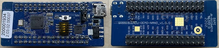
Purchase the development board from the Tuya Developer Platform. The part number of the
GR5515IENDU_DEMO_NANOdevelopment board is 2.03.02.00037.-
Schematic diagram:
hardware\GR551x\module_manual\GR5515IENDU-DEMO-NANO_V1.0.0.pdf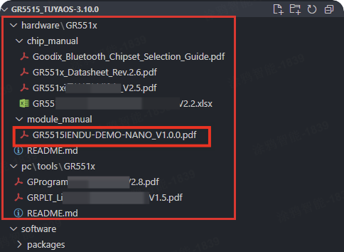
-
Pin multiplexing:
hardware\GR551x\module_manual\GR5515 (Pinmux).xlsx
-
Peripherals
Visit the Goodix website for GR551x chip features and specifications.
-
GPIO
GR5515I and GR5513 have 39 and 22 GPIO pins for multiplexing, respectively, as shown below. For more information, see Pin Mux in
hardware\GR551x\chip_manual\GR551x_Datasheet_Rev.2.3.pdf.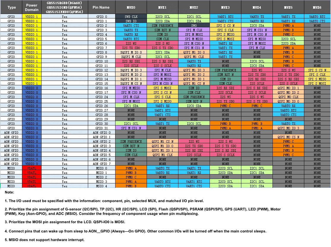
The table below shows the mapping between pin numbers and GR551x pin names.
Pin number GR551x_pin Pin number GR551x_pin Pin number GR551x_pin TUYA_GPIO_NUM_0 GPIO_0 TUYA_GPIO_NUM_32 AON_GPIO_0 TUYA_GPIO_NUM_40 MSIO_0 TUYA_GPIO_NUM_1 GPIO_1 TUYA_GPIO_NUM_33 AON_GPIO_1 TUYA_GPIO_NUM_41 MSIO_1 … … … … … … TUYA_GPIO_NUM_30 GPIO_30 TUYA_GPIO_NUM_38 AON_GPIO_6 TUYA_GPIO_NUM_43 MSIO_3 TUYA_GPIO_NUM_31 GPIO_31 TUYA_GPIO_NUM_39 AON_GPIO_7 TUYA_GPIO_NUM_44 MSIO_4 -
UART
GR551x has UART0 and UART1. See the pin multiplexing table for mapping UARTs to GPIOs.
The default UART definitions for TuyaOS SDK are shown below. Custom pin configurations are supported.
UART Feature Pin Description UART0 TX GPIO_0 Firmware flashing, authorization, and debugging ( APP_UART_ID_0)
Flip the second DIP switch to the ON position (towards the main chip).UART0 RX GPIO_1 Flip the first DIP switch to the ON position (towards the main chip). UART1 TX MSIO_0 Log output ( APP_UART_ID_1)
Flip the fourth DIP switch to the ON position (towards the main chip).
You can connect M0 to G10 to use the onboard serial port (G10 connects to the onboard serial port chip via the DIP switch).UART1 RX MSIO_1 Reserved In some older versions of the TuyaOS SDK, the default pin definition for UART1 may vary. For details, please check the default UART1 mapped pins in
tkl_uart.cwithin the SDK. -
SPI
GR551x has two SPI interfaces (one SPI controller interface with two peripheral chip select pins + one SPI peripheral interface), up to 32 MHz. The SPI controller interface is used by default. You can connect the MISO and MOSI signals together (that is, short the G25 and G16) to perform a loopback test. The default pin definitions:
SPI Feature Pin SPIM CS GPIO_17 (G17) SPIM CLK GPIO_24 (G24) SPIM MOSI GPIO_25 (G25) SPIM MISO GPIO_16 (G16) -
I2C
GR551x has two I2C interfaces, supporting 100 kHz, 400 kHz, 1 MHz, and 2 MHz. To display SDK information (TuyaOS demo), the OLED is pre-initialized. I2C0 is used by default.
I2C Feature Pin I2C0 SCL GPIO_30 (G30) I2C0 SDA GPIO_26 (G26) -
PWM
GR551x supports 6-channel PWM output.
Channel GR5515 pin GR5513 pin Notes 0 MSIO_0 (M0) GPIO_2 (G2) PWM0_A 1 MSIO_1 (M1) GPIO_3 (G3) PWM0_B 2 MSIO_2 (M2) GPIO_4 (G4) PWM0_C 3 GPIO_7 (G7) GPIO_31 (G31) PWM1_A 4 GPIO_10 (G10) GPIO_30 (G30) PWM1_B 5 GPIO_11 (G11) GPIO_26 (G26) PWM1_C -
ADC
13-bit ADC, up to 1 Msps, eight channels (five external test channels and three internal signal channels), supporting both single-ended and differential inputs. GR5515 and GR5513 adapt five and two channels of external analog single-ended input, respectively.
Channel GR5515 pin GR5513 pin 0 MSIO_0 (M0) MSIO_0 (M0) 1 MSIO_1 (M1) MSIO_1 (M1) 2 MSIO_2 (M2) None 3 MSIO_3 (M3) None 4 MSIO_4 (M4) None -
Key control
AON_GPIO_0(A0) applies to TuyaOS SDK v3.9.0 and later.AON_GPIO_6(A6) applies to TuyaOS SDK v3.8.3 only.- Press the button to wake up the device.
- Press and hold the button for five seconds to factory reset the device.
-
Startup time detection pin
GPIO_5 (G5)Set this pin to high after entering the
mainfunction.
Software environment
Install Keil and GR551x-dependent environment.
Keil
-
Download Keil from the Arm Keil website. mdk528a.exe is recommended. During installation, keep all the default settings.
-
If you are prompted to install a driver, continue with Install.
-
When opening Keil, if you are prompted to install a software pack, close the window.
-
After Keil is installed, add the path of the
UV4.exefile to the environment variable. For example,TUYAOS_COMPILE_TOOL:C:\Keil_v5\UV4, as shown below.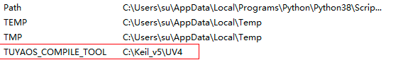
VSCode development
This platform supports both the Visual Studio Code development environment provided by Tuya and the Keil development environment provided by the chip original manufacturer.
For detailed instructions on using the Visual Studio Code development environment, please refer to Get development framework and Build development framework.
GProgrammer
GProgrammer is a firmware flashing tool that applies to GR551x and GR5526 series. It supports features such as debugging, firmware download, flash read/write, eFuse download, and firmware encryption and signing. In mass production, you can use PLT Lite and GRPLT Lite Config Tool to program and test GR551x and GR5526 series in bulk.
The steps to install GProgrammer are as follows, taking Windows as an example.
-
Visit Goodix website and download GProgrammer (Windows). V1.2.36 or later is recommended.
-
Keep all the default settings and complete the installation.
Develop software
Select chip type
GR551x series offers various packaging types to support diverse applications. CHIP_TYPE supports GR5515 and GR5513. When you develop with different chip platforms, you need to alter the chip type in custom_config.h accordingly.
// <o> Select chip type
// <0=> GR5515
// <1=> GR5513
#ifndef CHIP_TYPE
#define CHIP_TYPE  0
#endif
Flash and RAM footprint
-
Disable the testing feature.
#define TUYA_SDK_TEST 0 -
Disable Tuya logging.
#define ENABLE_LOG 0 #define BOARD_ENABLE_LOG 0 -
After a full compilation of the whole project, open the
.mapfile. You will get the RAM and flash footprint.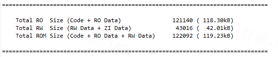
Firmware flashing
Wire connection
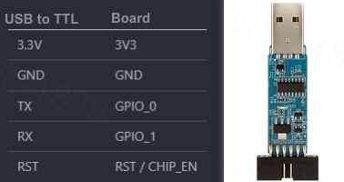
GR5515ENDU_DEMO_NANO development board comes with a USB to TTL serial port, which can be used for firmware flashing. Connect the hardware and flip all DIP switches to the ON position (towards the GR551x main controller). During the process, the reset operation is done manually.
Before flashing firmware, you need to unlock the flash. Several reset operations are needed in a complete flashing and authorization process. Therefore, it is recommended to connect the RST signal to the chip reset pin using a USB to TTL adapter. This enables the script or host to control the RST pin automatically.
Firmware description
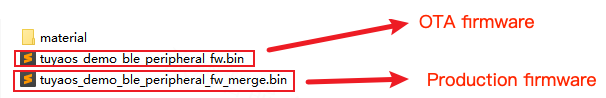
For more information about the compilation output and firmware flashing guide, see .\hex\material\README.md.
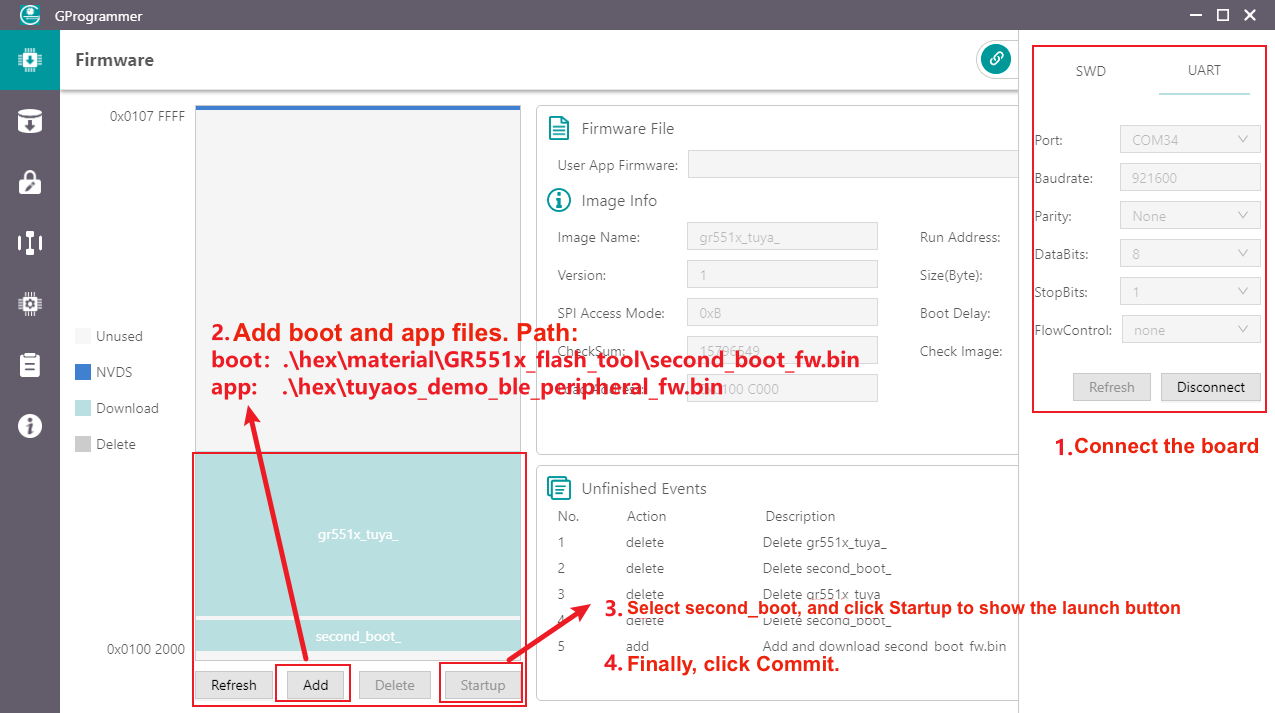
Flashing method 1: GProgrammer
SDK v3.9.0 and later support flash lock for the chip vendor. You need to unlock the flash before flashing the firmware. However, GProgrammer does not support unlocking the flash currently. When debugging, you can try the following options to unlock the flash.
- Use the command line. See Flashing method 2: Command-line tool.
- When debugging, comment out the flash protection function
hal_flash_block_protect(0, 0x0B)under themainfunction.
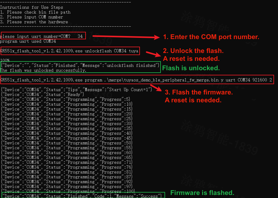
Flashing method 2: Command-line tool
The chip vendor’s flash tool GR551x_flash_tool_v1.2.42.1009.exe supports unlocking the flash.
Open .\hex\material\GR551x_flash_tools and double-click the script program.bat to run. If the board is connected to the RST signal, it will be reset automatically in the following process. Otherwise, a manual reset is required.
Features
Startup time
-
Use a logic analyzer to measure the signal time difference between the VCC pin and the startup time detection pin.
-
Detection pins: peripheral → startup time detection pin
-
Startup time: From power-on to the execution of the main function, it takes about one second, during which 0.5 seconds are used by the program embedded in the chip to detect the serial connection of GProgrammer.
Flash partition
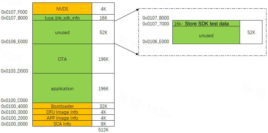
Adjust flash partitions
In the original project, you can modify the macros to adjust the default flash partitions.
- When the application code size exceeds the default 196 KB, you can compress the unused partition.
- When the unused partition that stores the business data is not enough, you can compress the application and OTA partitions.
- The unused partition stores testing data by default, which can be allocated to your needs.
- In principle, modifying the size of other partitions is not necessary or recommended.
Start address of applications
// custom_config.h

// <o> Code load address
// <i> Default: 0x01002000
#define APP_CODE_LOAD_ADDR      0x0100C000

// <o> Code run address
// <i> Default: 0x01002000
#define APP_CODE_RUN_ADDR       0x0100C000
Start address and size of OTA data
// board.h

#ifndef BOARD_FLASH_OTA_START_ADDR
#define BOARD_FLASH_OTA_START_ADDR    (0x0103D000)
#endif

#ifndef BOARD_FLASH_OTA_END_ADDR
#define BOARD_FLASH_OTA_END_ADDR    (0x0106E000)
#endif

#ifndef BOARD_FLASH_OTA_SIZE
#define BOARD_FLASH_OTA_SIZE        (BOARD_FLASH_OTA_END_ADDR - BOARD_FLASH_OTA_START_ADDR)
#endif
Unused partition
// board.h

// Address of SDK test data storage, 16K
/**@brief   Define storage SDK test data addr, such as storage bulk data, and product test common data. */
#ifndef BOARD_FLASH_SDK_TEST_START_ADDR
#define BOARD_FLASH_SDK_TEST_START_ADDR         (0x01077000)
#endif
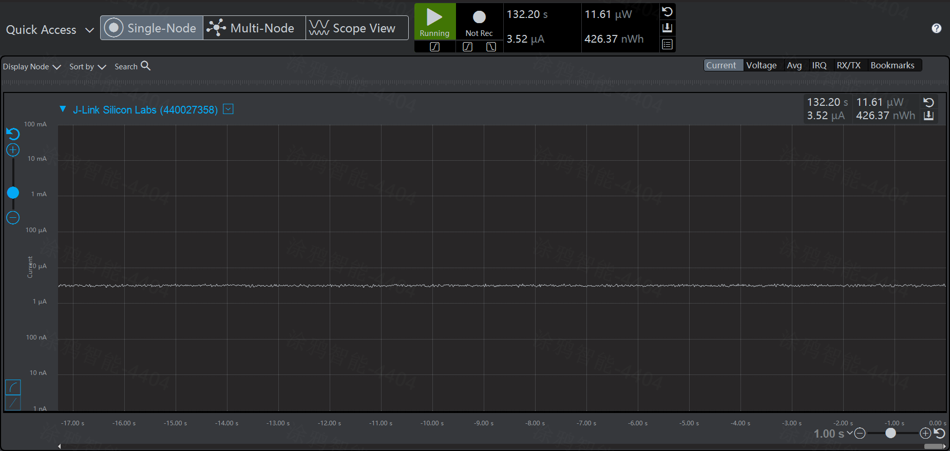
Power consumption
Test method
-
Remove the power indicator LED or series resistor on the NANO board.
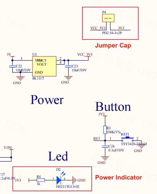
-
Flip the DIP switch of the USB to TTL converter chip to the OFF position (towards the jumper cap).
-
Disconnect all external cables except for the serial cable connected to the host. You can connect a USB to TTL converter to the serial port on the board. Connect the TX and RX of the USB serial port to
GPIO_1andGPIO_0respectively. -
Connect to an ammeter that can provide 3.3V of power, with its positive and negative terminals connected to the 3V3 pin and the GND pin on the board respectively.
-
You can measure the power consumption in different modes using power management in the host software.
Power consumption
-
Measure the average power consumption of typical one-second advertising.

-
Measure the average power consumption of typical 600-millisecond advertising.
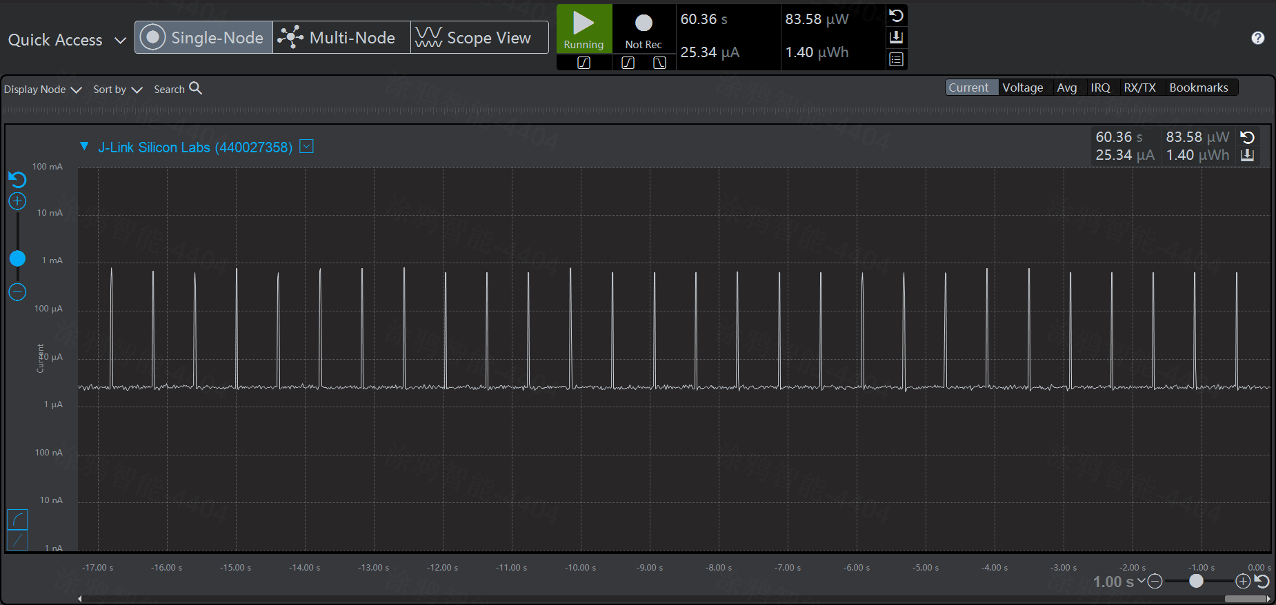
-
Measure the average power consumption of typical 200-millisecond advertising.
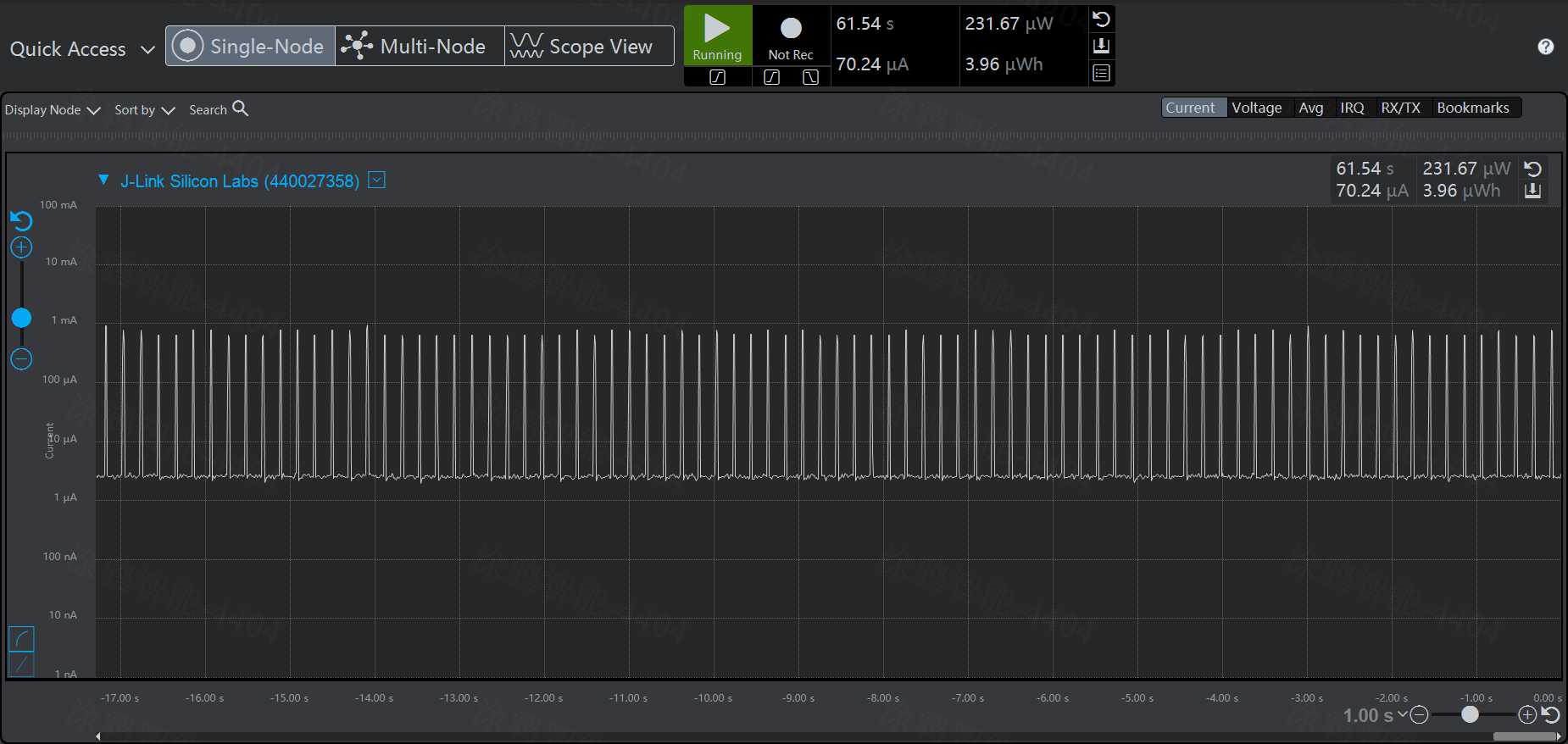
-
Measure the average power consumption in typical deep sleep mode, with all peripherals turned off, advertising disabled, AON wake-up enabled, and RAM data retained.
Local clock testing
The local clock has a time drift of less than one second after operating for over 50 hours.
Before the RTC test, calibrate the 32 MHz crystal oscillator to ensure the accuracy of the test result.
Is this page helpful?
YesFeedbackIs this page helpful?
YesFeedback


