Bluetooth LE-BG24
This topic describes the basics of the chip platform used in TuyaOS development. For more information, visit Tuya Developer Forum.
Hardware environment
Datasheet
- Method 1: After integrating the Bluetooth Sub-Device Development Framework, you can get the datasheet and reference manual in the
vendor\bg24_ble\documents\path. - Method 2: Visit the official website of Silicon Labs and get the latest information in the Documentation Center.
Development board
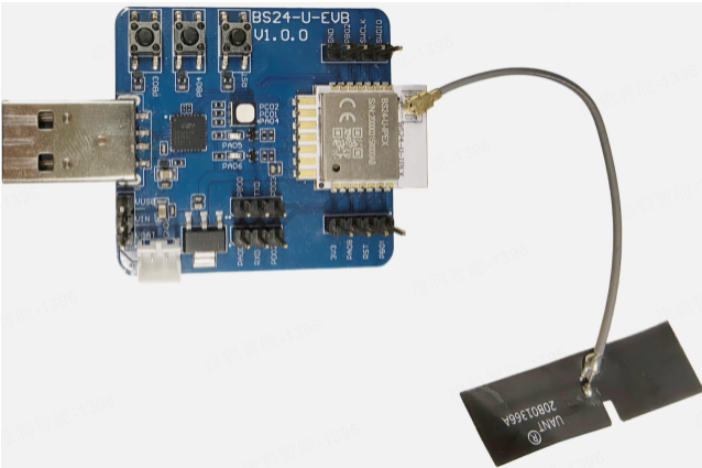
-
The following figure shows BS24-U-EVB:
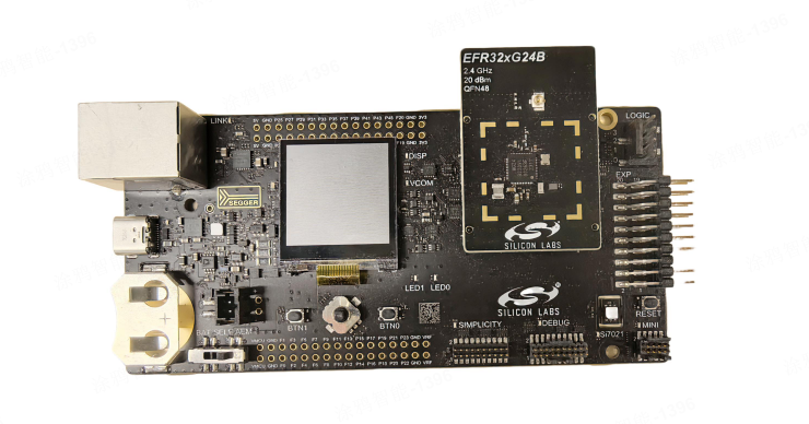
-
The following figure shows the development board from the chip vendor:
Peripherals
Peripherals and corresponding GPIOs
- As the module does not require all pins to be exposed, GPIO multiplexing occurs within the SDK.
- You can customize pin assignments in
board_gpio.haccording to your specific application requirements.
GPIO
The SDK defaults to using the EFR32BG24A020IM40 chip model. All peripheral descriptions below are based on this chip. To change to a 48-pin package, define BOARD_GPIO_MAX to 48 in the app_config.h file.
To operate a specific I/O in TuyaOS, you need to specify its pin number in the input parameter. For the BG24 series chip platform, the table below shows the mapping between GPIO numbers and physical I/O pins:
QFN40
| GPIO No. | Pin | GPIO No. | Pin |
|---|---|---|---|
| TUYA_GPIO_NUM_1 | PC00 | TUYA_GPIO_NUM_2 | PC01 |
| TUYA_GPIO_NUM_3 | PC02 | TUYA_GPIO_NUM_4 | PC03 |
| TUYA_GPIO_NUM_5 | PC04 | TUYA_GPIO_NUM_6 | PC05 |
| TUYA_GPIO_NUM_7 | PC06 | TUYA_GPIO_NUM_8 | PC07 |
| TUYA_GPIO_NUM_16 | PB04 | TUYA_GPIO_NUM_17 | PB03 |
| TUYA_GPIO_NUM_18 | PB02 | TUYA_GPIO_NUM_19 | PB01 |
| TUYA_GPIO_NUM_20 | PB00 | TUYA_GPIO_NUM_21 | PA00 |
| TUYA_GPIO_NUM_24 | PA03 | TUYA_GPIO_NUM_25 | PA04 |
| TUYA_GPIO_NUM_26 | PA05 | TUYA_GPIO_NUM_27 | PA06 |
| TUYA_GPIO_NUM_28 | PA07 | TUYA_GPIO_NUM_29 | PA08 |
| TUYA_GPIO_NUM_37 | PD03 | TUYA_GPIO_NUM_38 | PD02 |
| TUYA_GPIO_NUM_39 | PD01 | TUYA_GPIO_NUM_40 | PD00 |
QFN48
| GPIO No. | Pin | GPIO No. | Pin |
|---|---|---|---|
| TUYA_GPIO_NUM_1 | PC00 | TUYA_GPIO_NUM_2 | PC01 |
| TUYA_GPIO_NUM_3 | PC02 | TUYA_GPIO_NUM_4 | PC03 |
| TUYA_GPIO_NUM_5 | PC04 | TUYA_GPIO_NUM_6 | PC05 |
| TUYA_GPIO_NUM_7 | PC06 | TUYA_GPIO_NUM_8 | PC07 |
| TUYA_GPIO_NUM_9 | PC08 | TUYA_GPIO_NUM_10 | PC09 |
| TUYA_GPIO_NUM_18 | PB05 | TUYA_GPIO_NUM_19 | PB04 |
| TUYA_GPIO_NUM_20 | PB03 | TUYA_GPIO_NUM_21 | PB02 |
| TUYA_GPIO_NUM_22 | PB01 | TUYA_GPIO_NUM_23 | PB00 |
| TUYA_GPIO_NUM_26 | PA00 | TUYA_GPIO_NUM_27 | PA01 |
| TUYA_GPIO_NUM_28 | PA02 | TUYA_GPIO_NUM_29 | PA03 |
| TUYA_GPIO_NUM_30 | PA04 | TUYA_GPIO_NUM_31 | PA05 |
| TUYA_GPIO_NUM_32 | PA06 | TUYA_GPIO_NUM_33 | PA07 |
| TUYA_GPIO_NUM_34 | PA08 | TUYA_GPIO_NUM_35 | PA09 |
| TUYA_GPIO_NUM_43 | PD05 | TUYA_GPIO_NUM_44 | PD04 |
| TUYA_GPIO_NUM_45 | PD03 | TUYA_GPIO_NUM_46 | PD02 |
| TUYA_GPIO_NUM_47 | PD01 | TUYA_GPIO_NUM_48 | PD00 |
PWM
By default, there are five PWM channels, occupying three channels of Timer0 and two of Timer1. Both Timer0 and Timer1 are 32-bit timers.
| Channel | Pin |
|---|---|
| 0 | PC01 |
| 1 | PC02 |
| 2 | PA04 |
| 3 | PA05 |
| 4 | PA06 |
UART
The system defaults to using two UART groups, with UART0 mapped to USART0 and UART1 mapped to EUSART0. The EUSART (only two groups available) can be multiplexed as SPI, UART, or card reader interfaces. Here, only its UART functionality is utilized.
| UART | Feature | Pin | Remarks |
|---|---|---|---|
| UART0 | TX | PD03 | Authorization and testing |
| UART0 | RX | PD02 | - |
| UART1 | TX | PA00 | Demo not used |
| UART1 | RX | PB00 | - |
SPI
| SPI | Feature | Pin |
|---|---|---|
| SPI0 | CS | PC00 |
| SPI0 | CLK | PC03 |
| SPI0 | SDI | PA00 |
| SPI0 | SDO | PB00 |
ADC
The chip supports 16 input channels, each of which can be configured as positive input (posInput) and negative input (negInput) modes. By default, negInput is connected to ground (GND, suitable for single-ended sampling). All I/Os of PAx, PBx, PCx, and PDx can be mapped to the input ports of IADC. They can be configured as single-channel sampling or multi-channel auto-scanning sampling mode.
By default, the SDK only supports one ADC to optimize resource usage. For additional channels, you can configure them by yourself.
| Channel | Pin |
|---|---|
| 0 | PB02 |
I2C
The chip has two I2C interfaces, supporting 100 kHz, 400 kHz, and 1 MHz. To display SDK information (TuyaOS demo), the OLED is pre-initialized. I2C0 is used by default.
| I2C | Feature | Pin |
|---|---|---|
| IIC0 | SCL | PB02 |
| IIC0 | SDA | PB01 |
Key control
PB04:
- Press the key to wake up the device.
- Press and hold the key for three seconds to factory reset the device.
Startup time detection pin
PA08: Used for power-on startup time detection. It is set to a high level after entering the main function.
For more information, see vendor\bg24_ble\documents\bg24_QA.md.
Software environment
-
Make sure the
makecommand line tool has been installed in the environment, or search and installmake, configure the environment variables, and compile again. -
The SDK includes the pre-packaged Commander CLI tool (for flashing and log output), located at
vendor\bg24_ble\toolchain\software\commander. -
The toolchain is already integrated into the SDK, so there is no need to download it again.
Develop software
Select chip type
The default chip model used by the SDK is EFR32BG24A020IM40. If you need to replace it with a chip model in a 48-pin package, you must define BOARD_GPIO_MAX as 48 in the app_config.h file.
SDK footprint
Flash memory allocation: The allocated application region is 352 KB, with approximately 270 KB actually utilized.

Remarks
-
For more information on setting up the onboard GPIOs, be sure to refer to the documentation.
-
For flash memory allocation settings, refer to the document
bg24_flash.md: vendor\bg24_ble\documents.
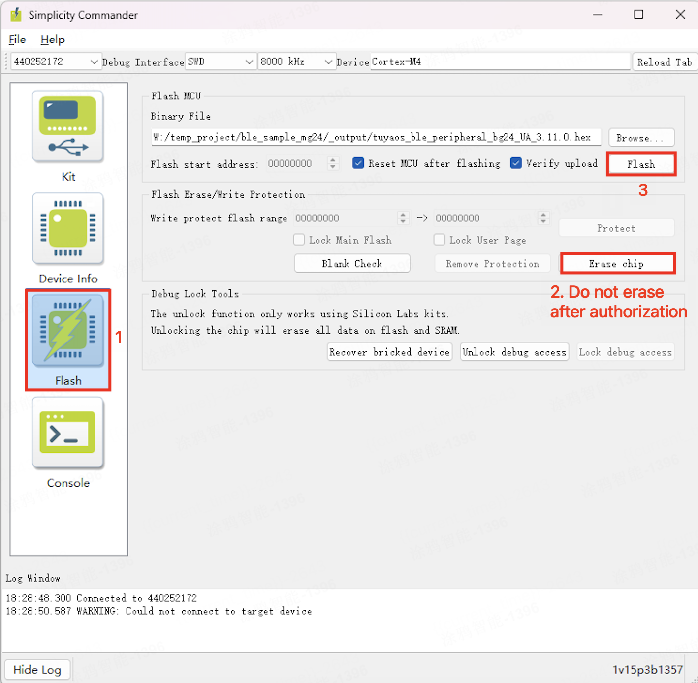
Flash firmware
Both firmware flashing and device logging are performed through the J-Link SWD interface.
-
Flash and erase: Click in the order shown below to perform the flash and erase operations.
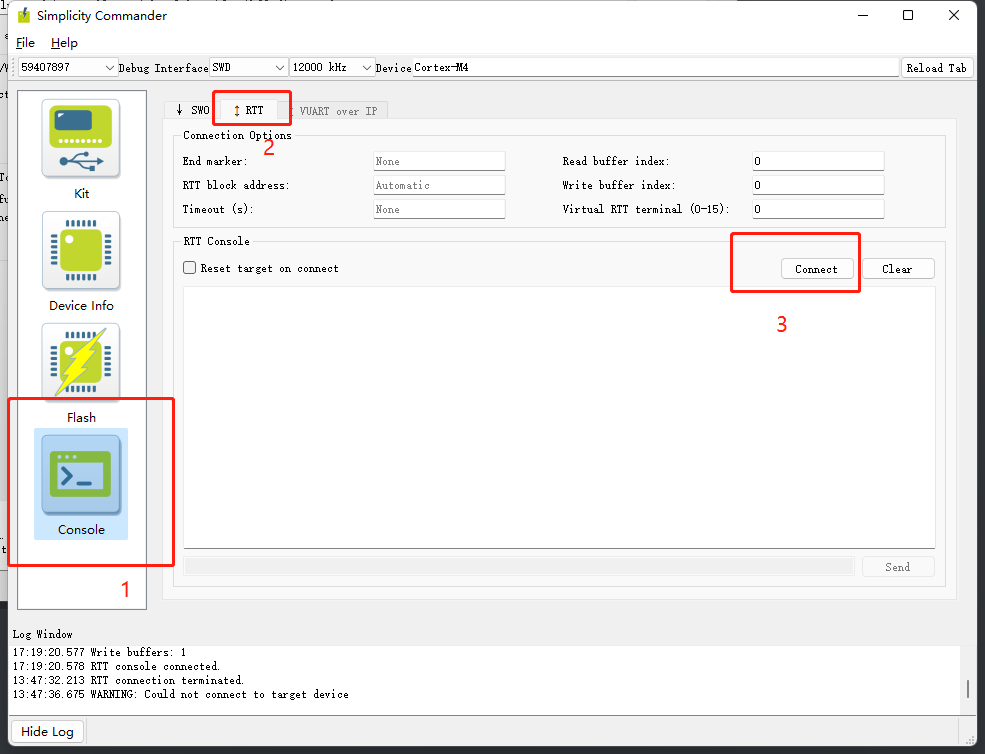
-
Logging system (RTT): Click in the order shown below to view the software running log and get debugging information. Alternatively, you can launch and run the J-Link RTT Viewer software.
Platform features
Flash partition
For more information, refer to the document bg24_flash.md: vendor\bg24_ble\documents.
| Feature name | Details | Address | Size | Remarks |
|---|---|---|---|---|
| bootloader(32 KB) | Bootloader | 0x0800 0000-0x0800 7FFF | 32 KB | The boot partition |
| Application firmware area (496 KB) | Application_Firmware | 0x0800 8000-0x0808 3FFF | 496 KB | Application code area |
| Update area(392 KB) | OTA backup | 0x0808 4000-0x0808 7FFF | 16 KB | Incremental restoration backup area |
| OTA patch (Firmware) | 0x0808 8000-0x080D FFFF | 352 KB | See note 1 | |
| OTA manage info | 0x080E 0000-0x080E 3FFF | 16 KB | OTA management information | |
| OTA breakpoint info | 0x080E 4000-0x080E 5FFF | 8 KB | Resumable download information | |
| Reserved area 1 (24 KB) | Reserved 1 data | 0x080E 6000-0x080E BFFF | 24 KB | Reserved area 1 |
| Bulk data area (16 KB) | Bulk data | 0x080E C000-0x080E FFFF | 16 KB | Bulk data storage area |
| Authorization data (32 KB) | Auth data | 0x080F 0000-0x080F 7FFF | 32 KB | See note 2 |
| NVM3 area (24 KB) | Bluetooth core Nvm3 | 0x080F 8000-0x080F EFFF | 24 KB | Original protocol stack storage area |
| Reserved area 2 (8 KB) | Reserved 2 data | 0x080F F000-0x080F FFFF | 8 KB | Reserved area 2 |
- Note 1: The firmware for this area can be divided into two categories:
- When configured for an incremental firmware update, this area contains the incremental firmware. The header of the last 16 KB of management information contains configuration details related to the incremental update. The incremental firmware size must not exceed 352 KB.
- When configured for a full firmware update, this area contains the full firmware. The size configuration for a full firmware differs from that of an application firmware. When using a full firmware update, pay attention to the firmware size. The default size for a full firmware is 352 KB.
Both methods support resumable (breakpoint) data transfer.
- Note 2: This area contains authorization information and must not be altered arbitrarily. Each set of authorization and configuration information is backed up. Therefore, there are four 8 KB blocks, totaling 32 KB.
Power consumption
Test method
-
Disconnect all external cables except for the serial cable connected to the host. You can connect a USB to TTL converter to the serial port on the board. Connect the TX and RX of the USB serial port to
PD02andPD03, respectively. -
Connect to an ammeter that can provide 3.3V of power. Connect the positive pole of the power supply to the VCC pin, and the negative pole to the GND on the board.
-
You can measure the power consumption in different modes using power management in the host software.
Power consumption
-
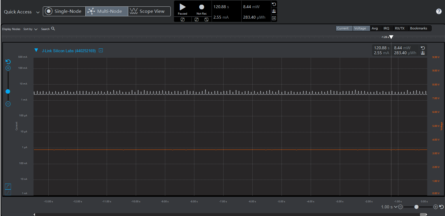
Broadcasting at 100 ms intervals results in approximately 2.5 mA typical power consumption.
-
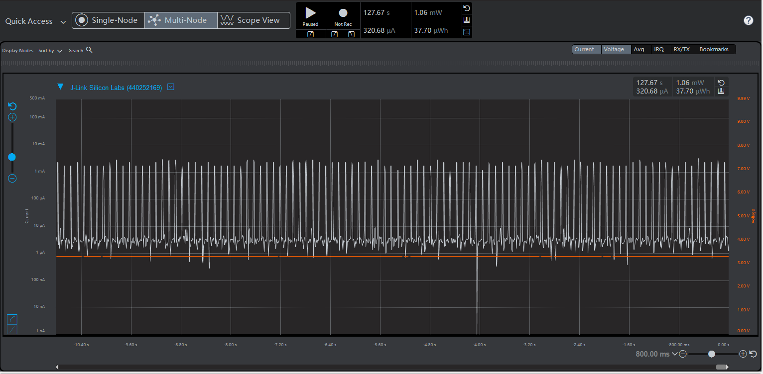
Low-power broadcasting at 100 ms intervals consumes approximately 320 μA in EM2 mode.
-
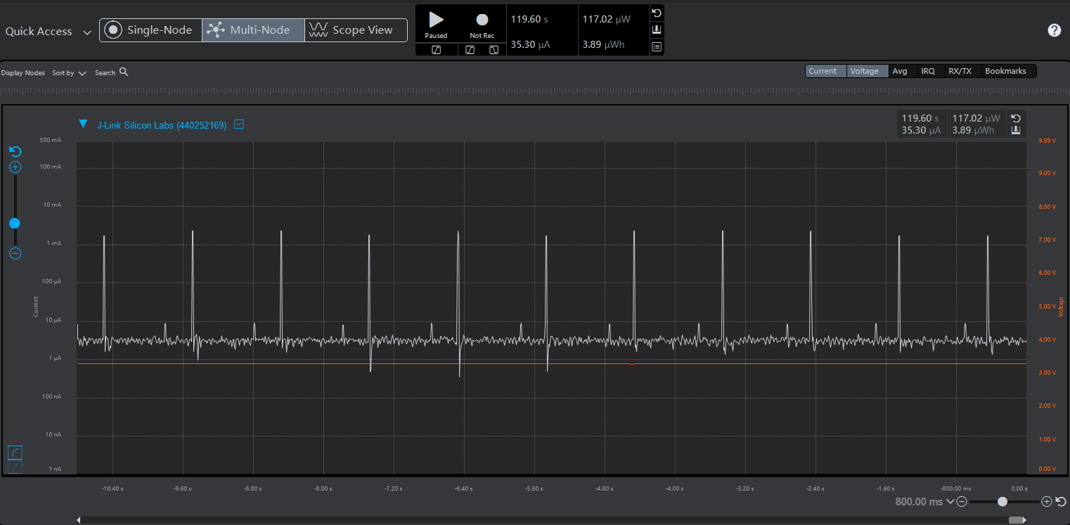
By default, 1-second interval broadcasting consumes approximately 35 μA.
-
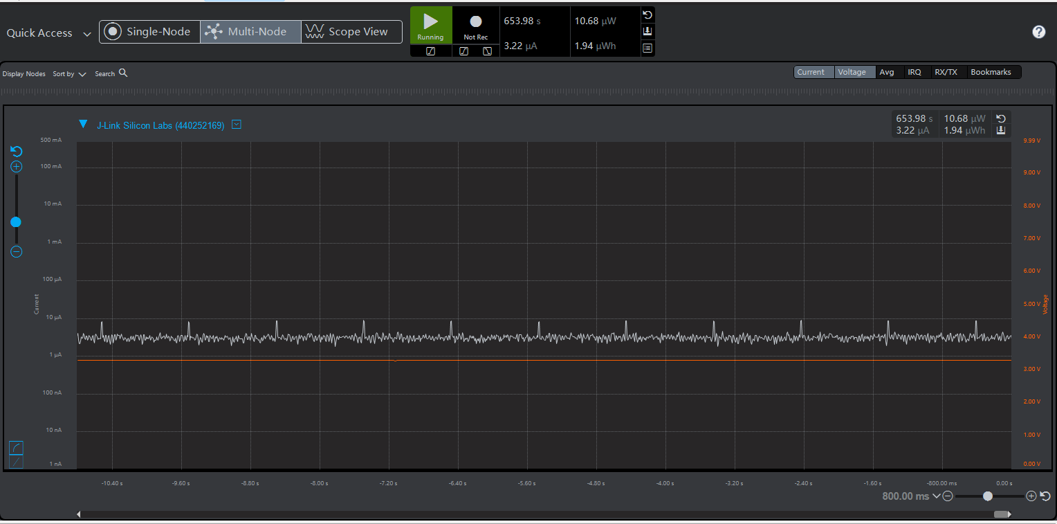
Without broadcasting, the EM2 power consumption is approximately 3.2 μA. Turn off all peripherals and advertising, maintain RTC and RAM data, and enable GPIO wake-up.
Is this page helpful?
YesFeedbackIs this page helpful?
YesFeedback


