Bluetooth LE–TLSR825x
This topic describes the basics of the TLSR825x chip platform used in TuyaOS development. For more information, visit Tuya Developer Forum.
Hardware environment
Chip
You can download the TLSR825x series datasheet from the Telink website.
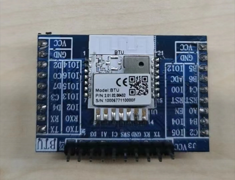
Development board
-
Core board: Built with Tuya’s BTU module.
-
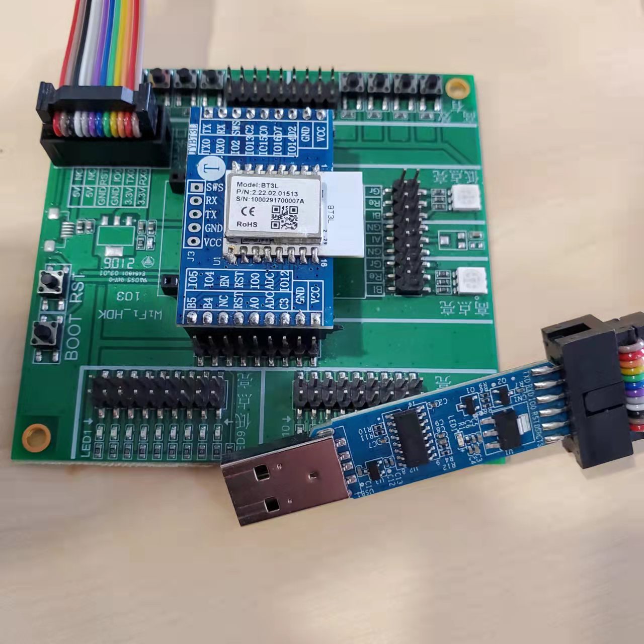
Motherboard:
Peripherals
GPIO
To operate a specific I/O in TuyaOS, you need to specify its pin number in the input parameter. Below is the pin mapping for the TLSR825x.
| Pin number | GPIO | Pin number | GPIO | Pin number | GPIO | Pin number | GPIO | Pin number | GPIO |
|---|---|---|---|---|---|---|---|---|---|
| 0 | PA0 | 8 | PB0 | 16 | PC0 | 24 | PD0 | 32 | PE0 |
| 1 | PA1 | 9 | PB1 | 17 | PC1 | 25 | PD1 | 33 | PE1 |
| 2 | PA2 | 10 | PB2 | 18 | PC2 | 26 | PD2 | 34 | PE2 |
| 3 | PA3 | 11 | PB3 | 19 | PC3 | 27 | PD3 | 35 | PE3 |
| 4 | PA4 | 12 | PB4 | 20 | PC4 | 28 | PD4 | - | - |
| 5 | PA5 | 13 | PB5 | 21 | PC5 | 29 | PD5 | - | - |
| 6 | PA6 | 14 | PB6 | 22 | PC6 | 30 | PD6 | - | - |
| 7 | PA7 | 15 | PB7 | 23 | PC7 | 31 | PD7 | - | - |
UART
This platform has one UART, the UART0. TuyaOS uses UART0 by default. To configure other pins as UART, see the TLSR825x Series Datasheet for details.
| UART | Feature | Pin |
|---|---|---|
| UART0 | TX | PB1 |
| UART0 | RX | PB7 |
SPI
This platform has two SPI buses, but only one can be used at a time. SPI1 is the default SPI bus in TuyaOS.
| SPI | Feature | Pin |
|---|---|---|
| SPI1 | CS | PD6 |
| SPI1 | CLK | PA4 |
| SPI1 | SDI | PA3 |
| SPI1 | SDO | PA2 |
| SPI2 | CS | PD2 |
| SPI2 | CLK | PD7 |
| SPI2 | SDI | PB6 |
| SPI2 | SDO | PB7 |
I2C
This platform has four I2C buses, but only one can be used at a time. I2C0 is the default I2C bus in TuyaOS.
| I2C | Feature | Pin |
|---|---|---|
| I2C0 | SCL | PC3 |
| I2C0 | SDA | PC2 |
| I2C1 | SCL | PC0 |
| I2C1 | SDA | PC1 |
| I2C2 | SCL | PB6 |
| I2C2 | SDA | PD7 |
| I2C3 | SCL | PA3 |
| I2C3 | SDA | PA4 |
PWM
This platform supports 6-channel PWM output. The default PWM pins after initialization are shown below. You can call tkl_pwm_mapping_to_gpio to change the GPIO mapped to PWM.
| Channel | Pin |
|---|---|
| 0 | PC2 |
| 1 | PC3 |
| 2 | PD4 |
| 3 | PD2 |
| 4 | PB4 |
| 5 | PB5 |
ADC
This platform has 10 pins for ADC multiplexing.
| Channel | Pin |
|---|---|
| 0 | PB0 |
| 1 | PB1 |
| 2 | PB2 |
| 3 | PB3 |
| 4 | PB4 |
| 5 | PB5 |
| 6 | PB6 |
| 7 | PB7 |
| 8 | PC4 |
| 9 | PC5 |
Firmware flashing
Wire connection
Connect the SWM pin on the programmer to the SWS pin on the module.
Firmware description
The production firmware and the OTA update use the same .bin file.
Flashing method 1
Upload the firmware file to the Tuya Developer Platform and use Tuya’s flashing and authorization tool. For more information, see Network Module.
Flashing method 2
Use Telink Burning and Debugging Tool (BDT). For more information, see Burning and Debugging Tools for all Series.
Features
Enable scanning
-
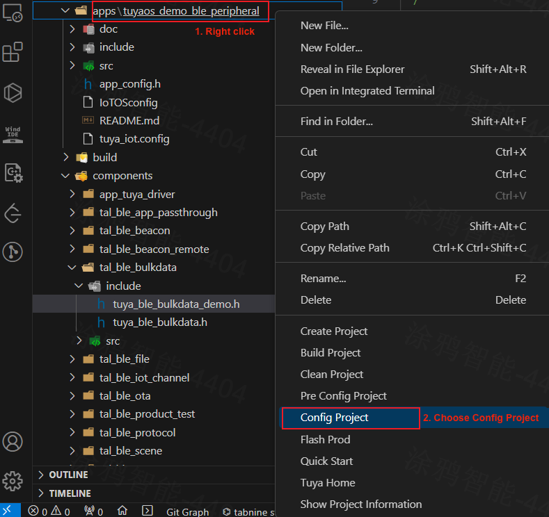
Add the following configuration item at the bottom of the file
apps\tuyaos_demo_ble_peripheral\IoTOSconfig.config ENABLE_SCAN bool "ENABLE_SCAN" default y -
Right-click the project directory and choose Config Project to make the changes take effect.
Storage
-
Flash memory: 512 KB
-
RAM: 48 KB (32 KB retention)
TLSR825x flash partitions:
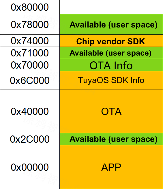
The Bluetooth LE SDK uses a dual backup scheme for firmware updates, with two partitions allocated to the firmware.
- Address range of the first partition: 0x00000 to 0x2B000. Given the chip design, reserve 4 KB memory space and do not use it.
- Address range of the second partition: 0x40000 to 0x6B000. Given the chip design, reserve 4 KB memory space and do not use it.
On power-up, the bootloader checks the availability of the firmware on the two partitions to determine which one should be run. If the firmware on both partitions is available, the first partition is run.
User space:
- 0x2C000 to 0x40000
- 0x71000 to 0x74000
- 0x78000 to 0x80000
Low power
Bluetooth devices have two low power modes: suspend sleep and deep sleep. Deep sleep consumes less power than suspend sleep.
How to enter sleep mode:
The sleep mode is subject to both the application layer and Bluetooth stack.
-
Application layer:
The application layer can activate sleep mode on the chip by running this function.
tal_cpu_allow_sleep()This only indicates that the application layer allows the chip to sleep. The decision to enter sleep, suspend sleep, or deep sleep mode depends on the current status of the Bluetooth stack.
-
Bluetooth stack:
After the application layer sets the sleep function, the Bluetooth stack decides whether to enter sleep mode after finishing its tasks. If the condition is not met, the chip will not enter sleep mode in the current loop. If the condition is met, the chip will enter sleep mode until the next task from the software timer or Bluetooth stack is due.
-
Things to know:
-
After calling
VOID_T tal_cpu_allow_sleep(VOID_T), the chip will automatically enter sleep mode when the sleep condition is met. -
All chip modules lose power during deep sleep. Therefore, after the chip wakes up from deep sleep, you need to initialize internal peripherals (GPIO, I2C, SPI, PWM, and UART). You can include hardware peripheral initialization functions into
OPERATE_RET tuya_init_third(VOID_T). -
Interrupts do not work when the TLSR825x chips are sleeping. To enable I/O wake-up functionality, configure the wake-up feature.
OPERATE_RET tkl_wakeup_source_set(CONST TUYA_WAKEUP_SOURCE_BASE_CFG_T *param) -
The TLSR825x chips cannot maintain their output capability in deep sleep mode, only providing a weak signal level to external devices through pull-up and pull-down inputs.
-
If you want the chip to maintain I/O output capability during sleep mode, it can only enter suspend sleep. You can use the following function to set the sleep mode to suspend sleep.
tkl_cpu_sleep_mode_set(1, TUYA_CPU_SLEEP);
-
-
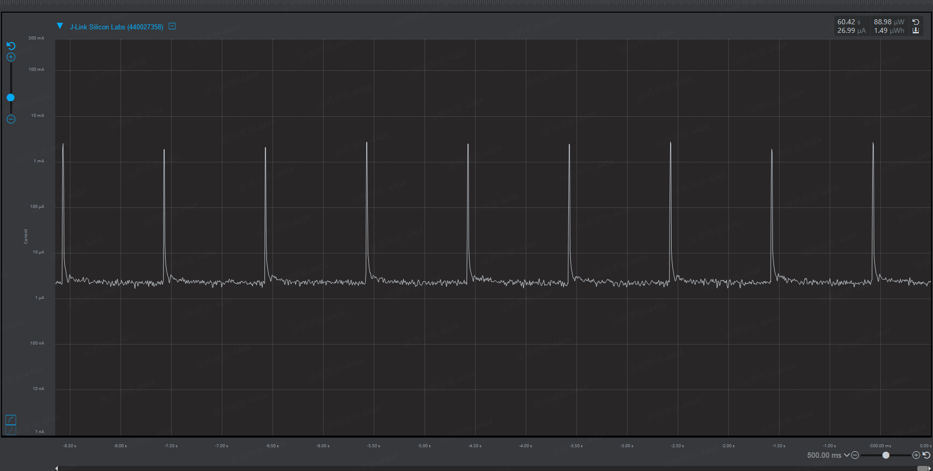
Power consumption at a 1,000 ms advertising interval
Is this page helpful?
YesFeedbackIs this page helpful?
YesFeedback


