Bluetooth LE–BK3633
This topic describes the basics of the chip platform used in TuyaOS development. For more information, visit Tuya Developer Forum.
Hardware environment
Chip datasheet
-
The datasheet can be found in
hardware\BK3633\chip_manual\BK3633_Datasheet_V1.5.pdf. -
Alternatively, check the Beken official website for the latest information.
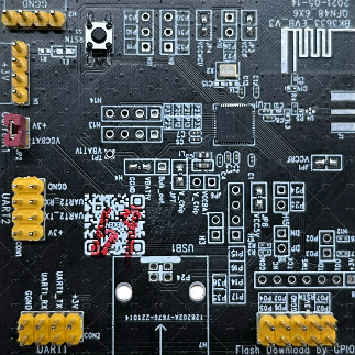
Development board
Development board from chip vendor
Peripherals
For BK3633 chip features and product parameters, visit the Beken official website.
-
GPIO
Three specification options are provided: 32 pins, 40 pins, and 48 pins. There are up to 32 GPIO pins that can be configured as input or output. GPIO pins can be reused for another feature. For more information, see 2 Pin Information and 3.2 GPIO in
hardware\GR551x\chip_manual\GR551x_Datasheet_Rev.2.3.pdf. The table below shows the mapping between pin numbers and BK3633 pin names.TUYA_GPIO_NUM definition Pin TUYA_GPIO_NUM_0 to TUYA_GPIO_NUM_07 P00 to P07 TUYA_GPIO_NUM_10 to TUYA_GPIO_NUM_17 P10 to P17 TUYA_GPIO_NUM_20 to TUYA_GPIO_NUM_27 P20 to P27 TUYA_GPIO_NUM_30 to TUYA_GPIO_NUM_37 P30 to P37 -
UART
The BK3633 platform has two non-configurable UART interfaces: UART0 and UART2. The table below shows the default pin definitions.
UART Feature Pin Description UART0 TX P00 Used to flash firmware and license and connect to a host for testing.
The baud rate defaults to 9600.UART0 RX P01 - UART2 TX P16 Used to print logs.
The baud rate defaults to 115200.UART2 RX P17 - -
SPI
The BK3633 platform has one SPI interface, supporting controller and peripheral modes, operating at speeds up to 32 MHz, with a frequency range of 126 kHz to 32 MHz.
The SPI controller interface is used by default. You can connect the MISO and MOSI signals together (that is, short the P06 and P05) to perform a loopback test. The default pin definitions:
SPI Feature Pin SPI0 CS P07 SPI0 CLK P04 SPI0 MOSI P05 SPI0 MISO P06 -
I2C
The BK3633 platform has one I2C interface, supporting 100 kHz and 400 kHz. SDK configuration only supports I2C controller mode, 7-bit addressing, and 1-byte register addresses. For special requirements, modify the software driver by referring to
i2c_software_drv.c. To display SDK information (TuyaOS demo), the OLED is pre-initialized. I2C0 is used by default.I2C Feature Pin I2C0 SCL P02 I2C0 SDA P03 -
PWM
The BK3633 platform supports 6-channel PWM output, channels 0 to 5. The SDK uses a 16 MHz main crystal oscillator as the default clock, operating within a frequency range of 1 Hz to 8 MHz. The table below lists the mapping between the channel and the default pin.
Channel Pin 0 P10 1 P11 2 P12 3 P13 4 P14 5 P15 -
ADC
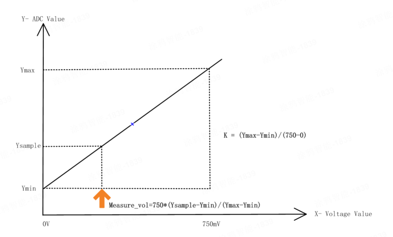
10-bit ADC, eight channels (five external test channels and three internal signal channels), supporting single and continuous modes. The external channel supports a voltage range of 0 to 1.05 V with an accuracy of ±50 mV. The table below lists the mapping between the channel and the pin.
Channel ADC source 0 Temperature sensor (not recommended) 1 P31 2 P32 3 P33 4 P34 5 P35 6 VBAT1V-pin 7 VCCBAT-pin How to improve ADC measurement accuracy:
-
To ensure consistent value conversion, add a 10 nF capacitor to ground on the ADC pin.
-
Perform linearity calibration on the hardware under test as instructed below:
-
Measure the VBAT reference. Connect a stable 3V power supply to VCCBAT and measure the ADC value of channel 7. The recorded value, referred to as Ymax, is the ADC value at the 0.75V point (VBAT/4). It is recommended to sample multiple boards from the same batch for accurate results.
-
Measure the zero point value. Connect channel 1 (P31) to the board’s GND and measure the ADC value of channel 1. The recorded value, referred to as Ymin, is the ADC value at 0 V. If you have multiple samples to test, repeat the process above.
-
Actual measurement. Measure the ADC value of channel x, referred to as Ysample. Convert the measurement to a voltage value in millivolts (mV) using the formula below.
V = 750 × (Ysample − Ymin) ÷ (Ymax − Ymin)
-
-
Input the reference value in
tkl_adc.c, as shown below.// The macro definition is located within the tkl_adc.c file. // Replace it with the actual measured values from the hardware. #define ADC_CALIC_VAL_0V ( 16 ) //!< ADC measurement value when connected to GND #define ADC_CALIC_VAL_0_75V ( 179 ) //!< Connect a standard 3V voltage to VCCBAT, and measure the ADC value.
-
-
Flash
Operation Time taken (ms) Erase 4 KB 8 ms Write 4 KB (erased) 35.8 ms Read 4 KB 6.89 ms 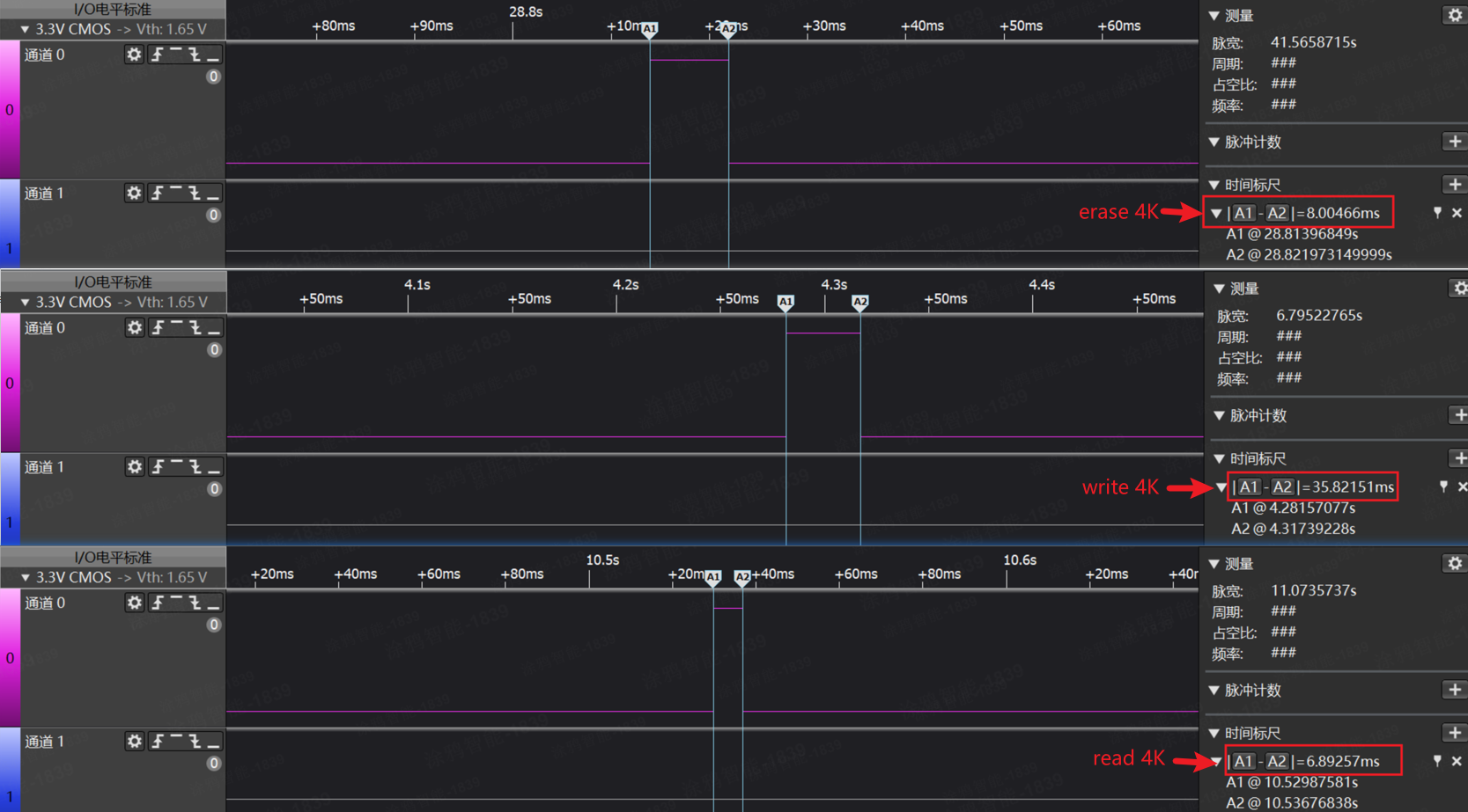
-
Key control
P32- Press the key to wake up the device.
- Press and hold the key for three seconds to factory reset the device.
-
Startup time detection pin
P31Set this pin to high after entering the
mainfunction.
Software environment
Install Keil and BK3633 flashing environment.
Keil
-
Download Keil from the Arm Keil website. mdk528a.exe is recommended. During installation, keep all the default settings.
-
If you are prompted to install a driver, continue with Install.
-
When opening Keil, if you are prompted to install a software pack, close the window.
-
After Keil is installed, add the path of the
UV4.exefile to the environment variable. For example,TUYAOS_COMPILE_TOOL: C:\Keil_v5\UV4, as shown below.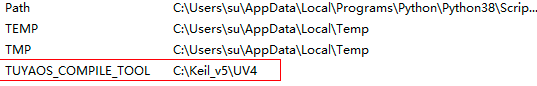
-
Install the legacy pack for Arm7, Arm9, and Cortex-R devices.
Visual Studio Code
The platform supports both the Visual Studio Code development environment provided by Tuya and the Keil development environment offered by the chip vendor.
For information on using the Visual Studio Code development environment, refer to Get development framework and Build development framework.
Flashing tool
You can flash firmware via serial port. Two flashing tool installers are available in .\vendor\bk3633_ble\sdk\BK3633_DesignKit_V06_2411\Tools\.
bk_writer_V2.00_20231218.exe- BKFIL (recommended)
Software development
Flash and RAM footprint
-
Disable the testing feature.
#define TUYA_SDK_TEST 0 -
Disable Tuya logging.
#define ENABLE_LOG 0 #define BOARD_ENABLE_LOG 0 -
After a full compilation of the whole project, open the
.mapfile. You will get the RAM and flash footprint.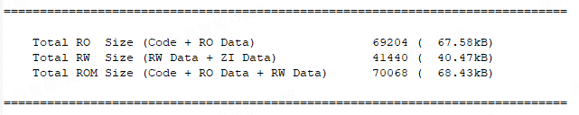
Firmware flashing
Wire connection
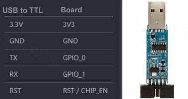
Connect the board’s power, ground, and UART0 (TX: P00, RX: P01) using a USB to TTL converter. Connect the RST signal to the chip reset pin. This enables the script or host to control the RST pin automatically.
Firmware description
The build output is located in .\log\output\app. BK3633 firmware consists of three parts: boot + stack + app.
-
tuyaos_demo_ble_peripheral_merge_crc.bin= boot + stack + app, the production firmware, supporting UART-based flashing. -
tuyaos_demo_ble_peripheral_oad.bin= app, the OTA update firmware, supporting UART-based flashing. -
tuyaos_demo_ble_peripheral_stack_oad.bin= stack + app, supporting UART-based flashing. Unless you need to upgrade the stack, this file is generally unnecessary.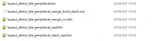
Flashing method 1: Chip vendor’s tool
Flash firmware using BKFIL
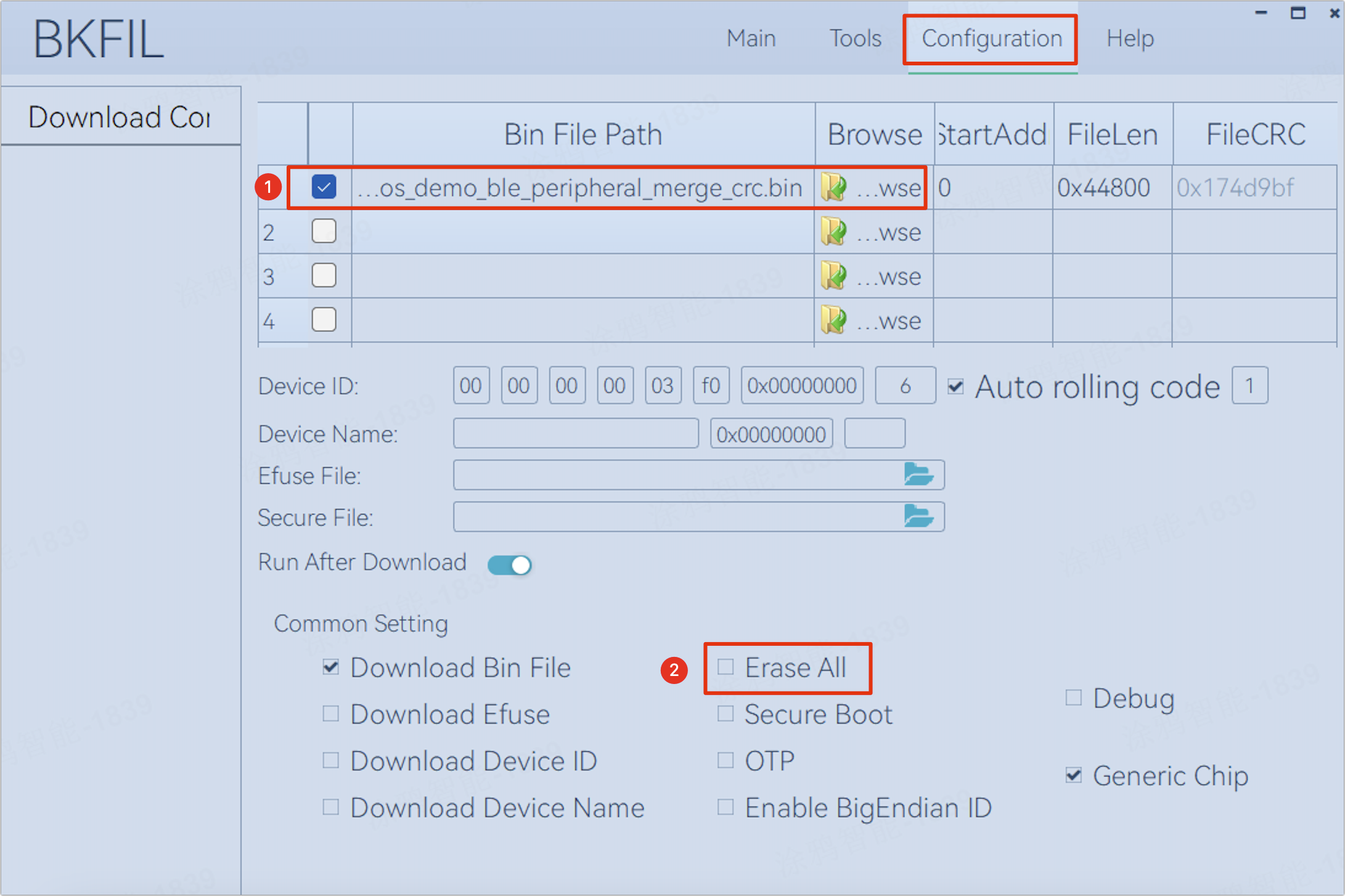
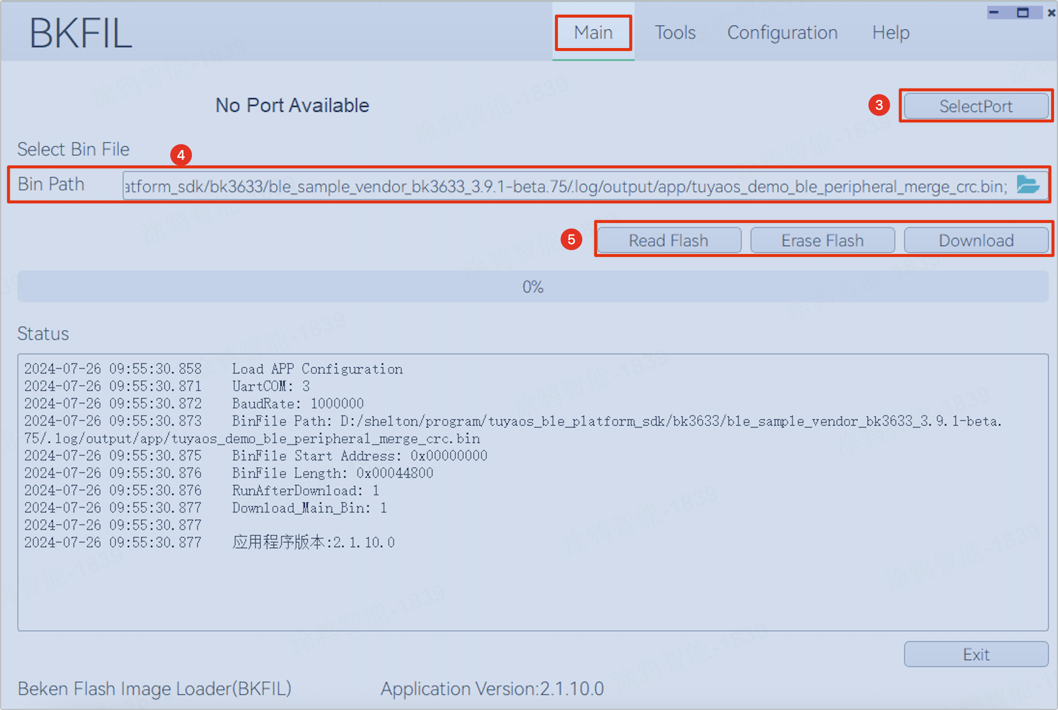
Instructions - Configuration and main screen
1: Select the binary file to flash. The selection will be synchronized to the Main screen.2: Erase All. If needed, check this option to erase the entire flash memory. If you update the code, there is no need to check it.3: Select Port. Select the serial port and set the baud rate to either 1M or 2M. Some serial modules do not support high baud rates. If issues occur, try lowering the baud rate.4: Select Bin file. You can also select the binary file on this screen.5: Actions. Download the code, erase the flash (erasing the code section only), and read the flash as needed.
Do not perform online updates for BKFIL. It is strongly recommended to use v2.1.10.0 from the TuyaOS development kit. Other versions might cause compatibility issues.
Flashing method 2: Tuya flashing tool
Tuya’s chip flashing host software supports the BK3633 platform.
Platform features
Startup time
-
Use a logic analyzer to measure the signal time difference between the VCC pin and the startup time detection pin.
-
Detection pins: peripheral → startup time detection pin.
-
Startup time: From power-on to the execution of the
mainfunction, it takes about 500 milliseconds.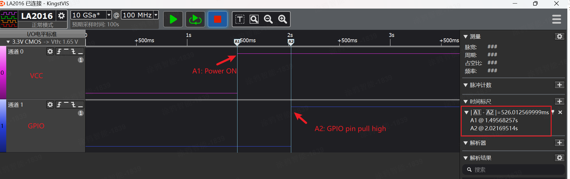
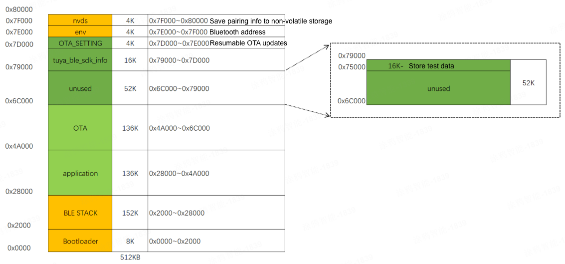
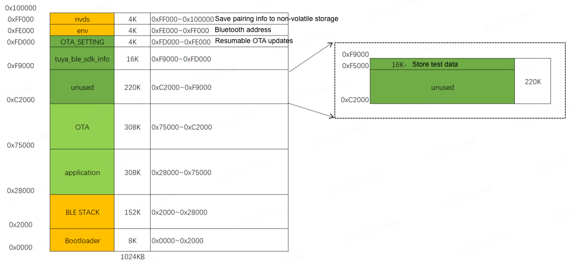
Flash partition
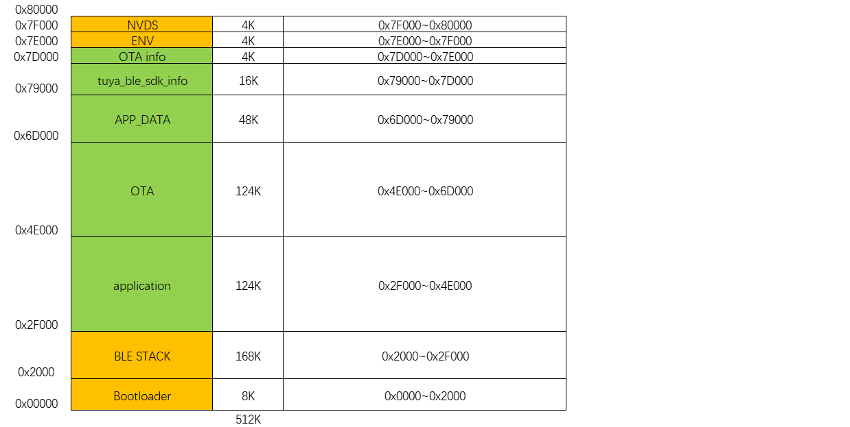
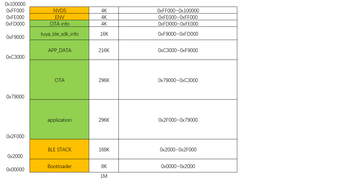
The BK3633 SiP flash supports either 512 KB or 1 MB. Define the flash specification for your chip by adding a macro in app_config.h, as shown below.
// app_config.h
#define BOARD_CHIP_TYPE 0  //!< 512KB Flash
#define BOARD_CHIP_TYPE 1  //!< 1MB Flash

// Flash
//<0=> 512K flash
//<1=> 1M flash
#ifndef BOARD_CHIP_TYPE
#define BOARD_CHIP_TYPE                         ( 0 )
#endif
The BK3633 TuyaOS Bluetooth Sub-Device Development Kit offers two versions: a Bluetooth Low Energy (LE) peripheral version and a dual-mode (peripheral & central) version, corresponding to the chip types BK3633 and BK3633_M in the development platform, respectively. Compared to the dual-mode version, the peripheral version reserves more flash space for application firmware and application data storage. Developers can choose the appropriate version based on the Bluetooth functional requirements of their specific projects.
512 KB flash partition (peripheral version)
1 MB flash partition (peripheral version)
512 KB flash partition (peripheral & central version)
1 MB flash partition (peripheral & central version)
Adjust flash partitions
In the original project, you can modify the macros in board.h to adjust the default flash partitions. The following examples provide several possible changes, using 512 KB as a reference.
-
When the
applicationcode size exceeds the default 136 KB, you can compress theunusedpartition. -
When the
unusedpartition that stores the business data is not enough, you can compress theapplicationand OTA partitions. -
The
unusedpartition stores testing data by default, which can be allocated to your needs. -
In principle, modifying the size of other partitions is not necessary or recommended.
After adjusting the flash partitions, update the parameters in the boot project located at
.\vendor\bk3633_ble\sdk\BK3633_DesignKit_V06_2411\SDK\projects\boot. See Adjust boot for details. Copy the generatedbk3633_boot.binand paste it into.\.log\output\bootto replace the existing file.
Start address and size of OTA data
// board.h

#if (BOARD_CHIP_TYPE == 0)
// 512 KB flash
#ifndef BOARD_FLASH_TUYA_INFO_START_ADDR
#define BOARD_FLASH_TUYA_INFO_START_ADDR        (0x79000)
#endif

#ifndef BOARD_FLASH_SDK_TEST_START_ADDR
#define BOARD_FLASH_SDK_TEST_START_ADDR         (0x75000)
#endif

#ifndef BOARD_FLASH_OTA_START_ADDR
#define BOARD_FLASH_OTA_START_ADDR              (0x4A000)
#endif

#ifndef BOARD_FLASH_OTA_END_ADDR
#define BOARD_FLASH_OTA_END_ADDR                (0x6C000)
#endif

#ifndef BOARD_FLASH_OTA_SETTING_ADDR
#define BOARD_FLASH_OTA_SETTING_ADDR            (0x7D000)
#endif

#ifndef BOARD_FLASH_OTA_SIZE
#define BOARD_FLASH_OTA_SIZE                    (BOARD_FLASH_OTA_END_ADDR - BOARD_FLASH_OTA_START_ADDR)
#endif

#else
// 1 MB flash
#ifndef BOARD_FLASH_TUYA_INFO_START_ADDR
#define BOARD_FLASH_TUYA_INFO_START_ADDR        (0xF9000)
#endif

#ifndef BOARD_FLASH_SDK_TEST_START_ADDR
#define BOARD_FLASH_SDK_TEST_START_ADDR         (0xF5000)
#endif

#ifndef BOARD_FLASH_OTA_START_ADDR
#define BOARD_FLASH_OTA_START_ADDR              (0x75000)
#endif

#ifndef BOARD_FLASH_OTA_END_ADDR
#define BOARD_FLASH_OTA_END_ADDR                (0xC2000)
#endif

#ifndef BOARD_FLASH_OTA_SETTING_ADDR
#define BOARD_FLASH_OTA_SETTING_ADDR            (0xFD000)
#endif

#ifndef BOARD_FLASH_OTA_SIZE
#define BOARD_FLASH_OTA_SIZE                    (BOARD_FLASH_OTA_END_ADDR - BOARD_FLASH_OTA_START_ADDR)
#endif

#endif
Unused partition
// board.h

// Storage address for SDK test data   16K
/**@brief   Define storage SDK test data addr, such as storage bulk data, and product test common data. */
// 512 KB flash
#ifndef BOARD_FLASH_SDK_TEST_START_ADDR
#define BOARD_FLASH_SDK_TEST_START_ADDR         (0x75000)
#endif

// 1 MB flash
#ifndef BOARD_FLASH_SDK_TEST_START_ADDR
#define BOARD_FLASH_SDK_TEST_START_ADDR         (0xF5000)
#endif
Adjust boot
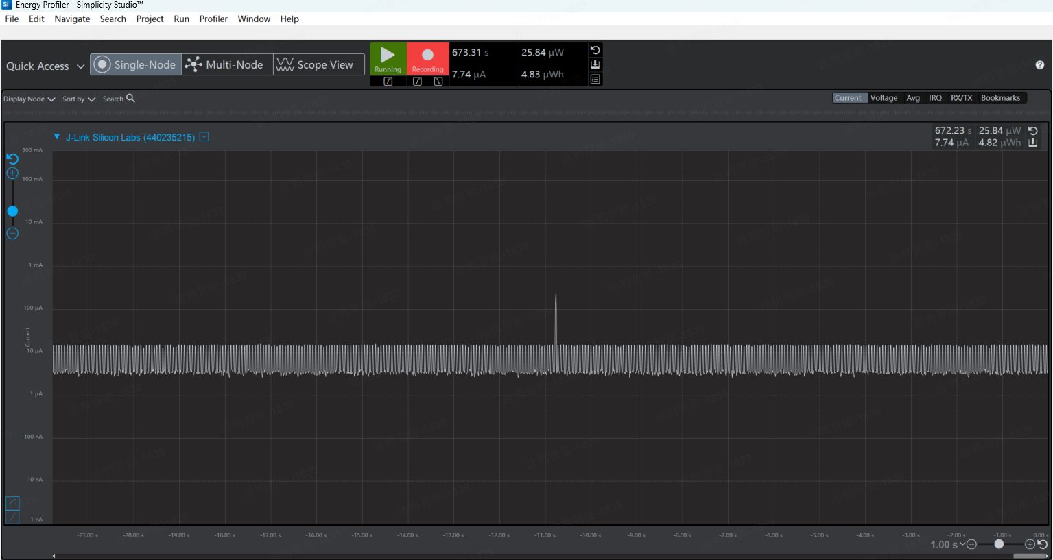
Power consumption
Test method
-
Disconnect all external cables except for the serial cable connected to the host. You can connect a USB to TTL converter to the serial port on the board. Connect the TX and RX of the USB serial port to
P01andP00, respectively. -
Connect to an ammeter that can provide 3.3 V of power. Connect the positive pole of the power supply to the +3 V silkscreen position, and the negative pole of the power supply to the GND on the board.
-
You can measure the power consumption in different modes using power management in the host software.
Power consumption
-
Measure the average power consumption of typical one-second advertising.
-
Measure the average power consumption of typical 600-millisecond advertising.
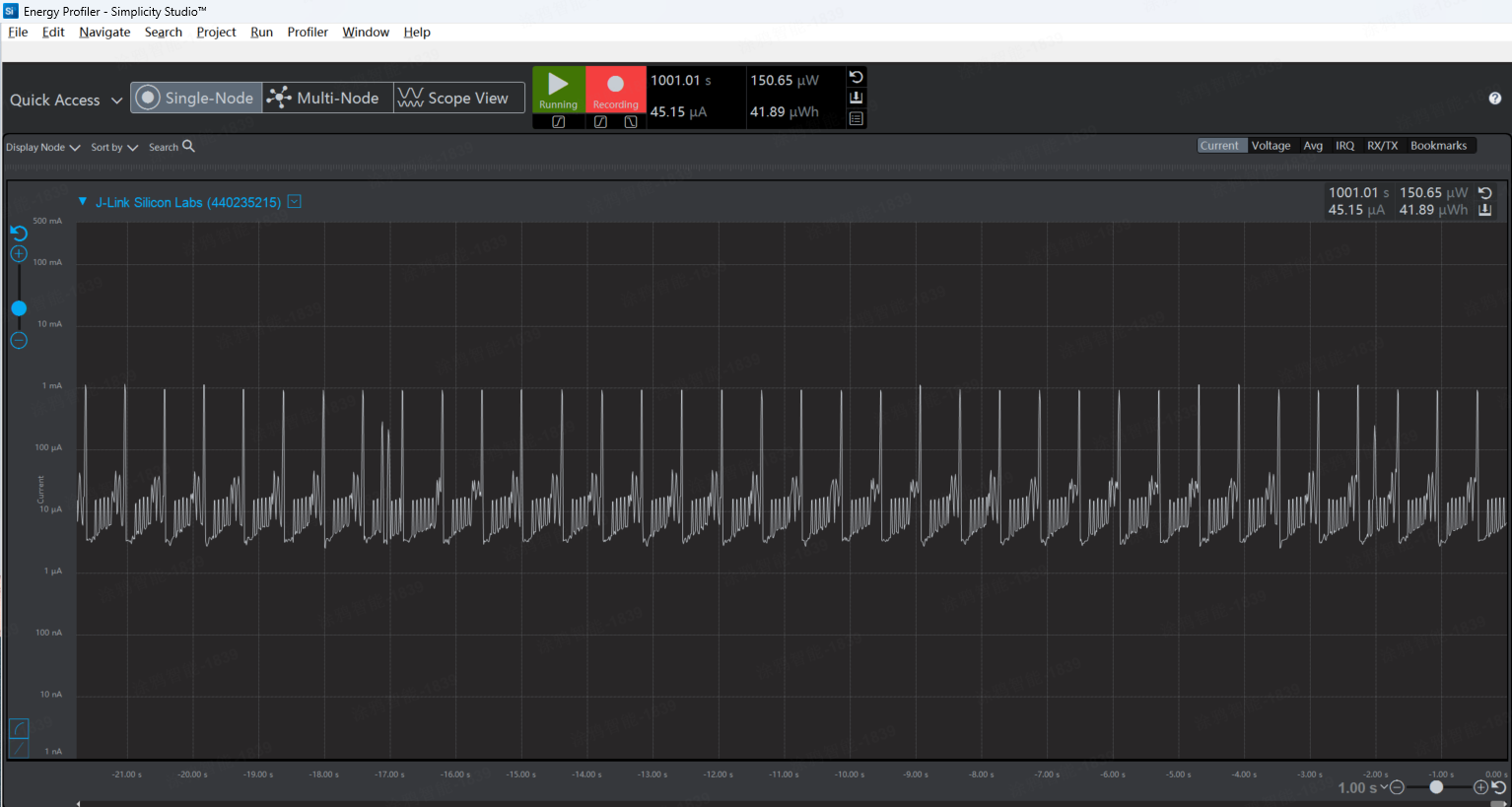
-
Measure the average power consumption in deep sleep mode. Turn off all peripherals and advertising, maintain RTC and RAM data, and enable GPIO wake-up.
Local clock testing
Choose the 32 kHz clock source for your hardware and specify it in board.h as shown below.
// 32K clock select, used inter RC32K set to 1, otherwise use external 32.768K crystal.
//<0=> external 32.768K crystal
//<1=> internal RC32K
#ifndef BOARD_USED_INTER_RC32K
#define BOARD_USED_INTER_RC32K                  (0)
#endif
QFN32 and QFN48 packages (Tuya custom version, P37) support connecting an external 32 kHz oscillator. Other package types lack the corresponding pin and default to using the external 32 kHz clock. It is recommended to use the crystal oscillator models specified by the chip vendor. The relevant datasheet is located in the TuyaOS Bluetooth Sub-device Development Kit/hardware folder.
Hardware testing: A development board from the chip vendor has a 16 MHz crystal oscillator with a frequency tolerance of ±20 ppm and connects to an external 32.768K crystal oscillator. The local clock has a time drift of about two seconds for 24 hours.
FAQs
BKFIL tool fails to launch
This occurs when the firmware file does not exist at the default path specified in the configuration. Delete the firmware path with BinFilePath="xxxxxx" in the settings.ini file in the folder where BKFIL.exe is located.
The device crashed during sleep mode
An exception occurred in the 32 kHz clock. The SDK defaults to using an external 32 kHz crystal oscillator. If the circuit board does not have an external crystal oscillator soldered, set the macro BOARD_USED_INTER_RC32K to 1 to enable the internal RC clock.
Device wake-up crash
The 16 MHz crystal oscillator failed to start up correctly. Use the crystal model recommended by the original manufacturer and include PCB footprints for load capacitors.
OTA reports success, but pre-upgrade firmware runs
Check and ensure that the OTA start address in the bootloader firmware matches the OTA start address configured in the application layer firmware.
Is this page helpful?
YesFeedbackIs this page helpful?
YesFeedback


