OM6626B Datasheet
Last Updated on : 2025-05-30 08:15:57download
Overview
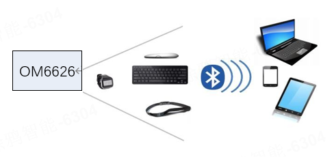
The OM6626 is a power-optimized true system-on-chip (SoC) solution for both Bluetooth low energy and proprietary 2.4GHz applications. It integrates a high-performance and low-power RF transceiver with a Bluetooth baseband and rich peripheral I/O extension. OM6626 also integrates a power management unit (PMU) to provide highly efficient power management. It targets 2.4GHz Bluetooth low energy systems, proprietary 2.4GHz systems, Human-Interface Devices (keyboard, mouse, and remote control), sports and leisure equipment, mobile phone accessories, and consumer electronics.
OM6626 on-chip Bluetooth system compatible with version 5.3.
The chip integrates up to 64MHz high-performance MCU, DMA, GPIO, SPI, UART, Timer, Watchdog, supports 32MHz external crystal, integrates multi-purpose max 12-bit ADC.
The OM6626 integrates on chip 80K SRAM, 256-bit EFUSE, and supports user-defined IDE system on chip SFLASH MCU development and JTAG software upgrade.
Features
- RF transceiver
- -98dBm sensitivity @ 1Mbps GFSK
- -95dBm sensitivity @ 2Mbps GFSK
- TX Power -30 to +8 dBm
- AGC (Auto Gain Control)
- RSSI (1dB Resolution)
- CPU and debug interface
- ARM® Cortex™-M4, max 64MHz
- SWD interface
- Memory
- EFUSE: 256-bit
- SRAM: 80KB
- Serial Flash: 1MB
- I-Cache RAM: 8KB
- Clocks
- 32MHz & 32.768kHz crystal oscillators
- 32MHz & 32.768kHz RC oscillators
- Link Controller
- BT 5.3 LE PHY, link controller
- Proprietary 2.4-GHz link controller
- Power Management
- Single power supply voltage: 1.71V ~ 3.6V
- 3.4mA peak current in RX
- 4.2mA peak current in TX (0 dBm)
- 1.2uA in sleep mode (with 16K RAM retention, 32 KHz RC)
- Integrated DCDC BUCK Converter
- Software
- Compatible with Bluetooth 5.3
- Supported data rates: 1Mbps, 2Mbps (BLE)
- Multiple configurable air data rates from 25 Kbps to 2 Mbps (2.4G)
- Supports mesh network
- Sample applications and profiles
- Supports OTA
- Peripherals
- Up to 25 General Purpose I/O pins
- 8 x DMA
- 2 x UART
- 1 x I2C interface (master only)
- 2 x SPI interface
- 1 x 16-bit Timer/Counter with 4 Compare/Capture/PWM channels
- 2 x 16-bit Timer/Counter with 4 Compare/PWM channels (These two timers can combine to one 32-bit PWM timer)
- 1 x 32-bit Real Time Counter with 3 Compare channels
- 1 x 16-bit Low Energy Timer with 2 Compare/PWM channels
- 1 x Watchdog Timer
- 8 channels single-end 12-bit GPADC, up to 333.3ksps (precision and sample rate can be configured)
- Security
- AES HW encryption
- Support AES-256/AES-128 key
- HW Random Number Generator
- AES HW encryption
- Package and Work Environment
- OM6626A: LGA28 3x3mm
- OM6626B: QFN32 4x4mm
- -40°C to +85°C
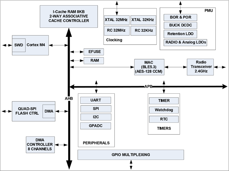
System function block diagram
OM6626 is a low-power Bluetooth wireless transceiver chip. The chip integrates Bluetooth baseband, PHY, and proprietary 2.4GHz protocol. The MCU accesses system hardware resources through the AHB bus, RAM, DMA, SFLASH, and GPIO exchange data through the AHB bus, and all other peripheral is accessed through the AHB to the APB Bridge and APB bus.
Applications
The OM6626 integrated circuit has a fully integrated radio transceiver and baseband processor for Bluetooth® Smart. It can be used as an application processor as well as a data pump in fully hosted systems.
Pinout
Pin diagram
The OM6626A is a 3mmx3mm LGA28 package. The chip pin definition is as below:
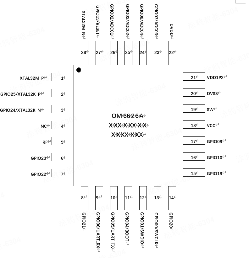
Note: The OM6626A has a pin in each corner (bottom view). Those pins are connected to the chip’s EPAD (Pin29) internally.
The OM6626B is a 4mmx4mm QFN32 package. The chip pin definition is as below:
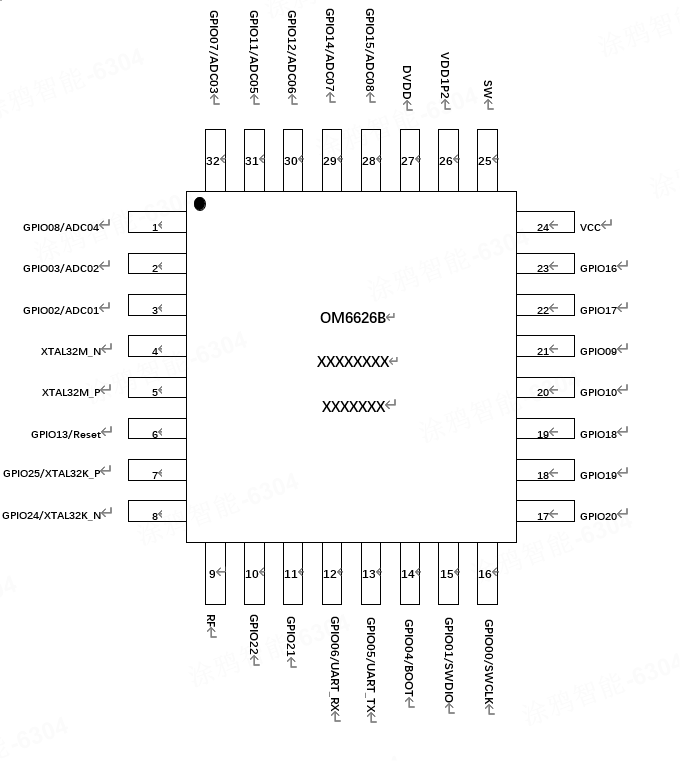
Note: The OM6626B has a pin in each corner (bottom view). Those pins are connected to the chip’s EPAD (Pin33) internally.
Pin description
OM6626A pin definition
| Name | Pin | Type | Description | Note |
|---|---|---|---|---|
| XTAL32M_P | 1 | Analog | 32M crystal oscillator P input | - |
| GPIO25/ XTAL32K_P | 2 | Digital/Analog | Digital GPIO/32.768K crystal oscillator P input | Note 1 |
| GPIO24/ XTAL32K_N | 3 | Digital/Analog | Digital GPIO/32.768K crystal oscillator N input | Note 1 |
| NC | 4 | NC | NC | - |
| RF | 5 | Analog | RF input/output | - |
| GPIO23 | 6 | Digital | Digital GPIO | Note 1 |
| GPIO22 | 7 | Digital | Digital GPIO | Note 1 |
| GPIO21 | 8 | Digital | Digital GPIO | Note 1 |
| GPIO06/UART_RX | 9 | Digital | Digital GPIO/UART_RX | Note 1 |
| GPIO05/UART_TX | 10 | Digital | Digital GPIO/UART_TX | Note 1 |
| GPIO04/BOOT | 11 | Digital | Digital GPIO/BOOT | Note 1 |
| GPIO01/SWDIO | 12 | Digital | Digital GPIO/SWDIO | Note 1 |
| GPIO00/SWCLK | 13 | Digital | Digital GPIO/SWCLK | Note 1 |
| GPIO20 | 14 | Digital | Digital GPIO | Note 1 |
| GPIO19 | 15 | Digital | Digital GPIO | Note 1 |
| GPIO10 | 16 | Digital | Digital GPIO | Note 1 |
| GPIO09 | 17 | Digital | Digital GPIO | Note 1 |
| VCC | 18 | Power | Power supply | - |
| SW | 19 | Analog | DCDC output connected to external inductance | - |
| DVSS | 20 | Power | Ground for digital | - |
| VDD1P2 | 21 | Power | Internal DCDC/LDO generated power supply | - |
| DVDD | 22 | Power | Internal LDO generated power supply for digital core | - |
| GPIO07/ADC03 | 23 | Digital/Analog | Digital GPIO/GPADC | Note 1 |
| GPIO08/ADC04 | 24 | Digital/Analo g | Digital GPIO/GPADC | Note 1 |
| GPIO03/ADC02 | 25 | Digital/Analog | Digital GPIO/GPADC | Note 1 |
| GPIO02/ADC01 | 26 | Digital/Analog | Digital GPIO/GPADC | Note 1 |
| GPIO13/Reset | 27 | Digital | Digital GPIO/Reset | Note 1/ (**) |
| XTAL32M_N | 28 | Analog | 32M crystal oscillator N input | - |
OM6626B pin definition
| Name | Pin | Type | Description | Note |
|---|---|---|---|---|
| GPIO08/ADC04 | 1 | Digital/Analo g | Digital GPIO/GPADC | Note 1 |
| GPIO03/ADC02 | 2 | Digital/Analo g | Digital GPIO/GPADC | Note 1 |
| GPIO02/ADC01 | 3 | Digital/Analo g | Digital GPIO/GPADC | Note 1 |
| XTAL32M_N | 4 | Analog | 32M crystal oscillator N input | - |
| XTAL32M_P | 5 | Analog | 32M crystal oscillator P input | - |
| GPIO13/Reset | 6 | Digital | Digital GPIO/Reset | Note 1/(**) |
| GPIO25/XTAL32K_P | 7 | Digital/Analo g | Digital GPIO/32.768K crystal oscillator P input | Note 1 |
| GPIO24/XTAL32K_N | 8 | Digital/Analo g | Digital GPIO/32.768K crystal oscillator N input | Note 1 |
| RF | 9 | Analog | RF input/output | - |
| GPIO22 | 10 | Digital | Digital GPIO | Note 1 |
| GPIO21 | 11 | Digital | Digital GPIO | Note 1 |
| GPIO06/UART_RX | 12 | Digital | Digital GPIO/UART_RX | Note 1 |
| GPIO05/UART_TX | 13 | Digital | Digital GPIO/UART_TX | Note 1 |
| GPIO04/BOOT | 14 | Digital | Digital GPIO/BOOT | Note 1 |
| GPIO01/SWDIO | 15 | Digital | Digital GPIO/SWDIO | Note 1 |
| GPIO00/SWCLK | 16 | Digital | Digital GPIO/SWCLK | Note 1 |
| GPIO20 | 17 | Digital | Digital GPIO | Note 1 |
| GPIO19 | 18 | Digital | Digital GPIO | Note 1 |
| GPIO18 | 19 | Digital | Digital GPIO | Note 1 |
| GPIO10 | 20 | Digital | Digital GPIO | Note 1 |
| GPIO09 | 21 | Digital | Digital GPIO | Note 1 |
| GPIO17 | 22 | Digital | Digital GPIO | Note 1 |
| GPIO16 | 23 | Digital | Digital GPIO | Note 1 |
| VCC | 24 | Power | Power supply | - |
| SW | 25 | Analog | DCDC output connected to external inductance | - |
| VDD1P2 | 26 | Power | Internal DCDC/LDO generated power supply | - |
| DVDD | 27 | Power | Internal LDO generated power supply for digital core | - |
| GPIO15/ADC08 | 28 | Digital/Analo g | Digital GPIO/GPADC | Note 1 |
| GPIO14/ADC07 | 29 | Digital/Analo g | Digital GPIO/GPADC | Note 1 |
| GPIO12/ADC06 | 30 | Digital/Analo g | Digital GPIO/GPADC | Note 1 |
| GPIO11/ADC05 | 31 | Digital/Analo g | Digital GPIO/GPADC | Note 1 |
| GPIO07/ADC03 | 32 | Digital/Analo g | Digital GPIO/GPADC | Note 1 |
Note 1: Refer to the pinmux diagram for the mapping between digital peripherals and GPIO.
(**): To ensure the Reset function, the pull-down time of the RSTB pin should be greater than 40us.
Recommended operation conditions
Absolute maximum ratings
| Parameter | Min | Typ | Max | Unit |
|---|---|---|---|---|
| Supply voltage (VCC) | -0.3 | - | 3.9 | V |
| Maximum Junction Temperature | -40 | - | 125 | ºC |
| Storage Temperature | -40 | - | 125 | ºC |
Normal operating conditions
| Rating | Min | Typ | Max | Unit |
|---|---|---|---|---|
| Operation Temperature | -40 | - | 85 | ºC |
| Digital Core supply voltage | 0.9 | 1.0 | 1.1 | V |
| Supply voltage (VCC) | 1.71 | 3.3 | 3.6 | V |
| I/O voltage | VCC | VCC | VCC | V |
ESD characteristic
| Parameter | Condition | Min | Typ | Max | Unit |
|---|---|---|---|---|---|
| Human Body Mode (HBM) | Test method: ESDA/JEDEC JS-001-2017 | - | 4000 | - | V |
| Machine Mode (MM) | All pins, test method: JESD22 -A115C | - | 200 | - | V |
| Charge Device Mode (CDM) | All pins, test method: ESDA/JEDEC JS-002-2018 | - | 1000 | - | V |
PMU
Power management
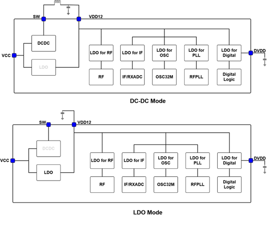
The main supply voltage is connected to the VCC pins. The system contains one main supply regulator stage, which has the following regulator type options:
- Low-dropout regulator (LDO)
- Buck regulator (DC/DC)
Main voltage regulator
By default, the LDO regulator is enabled and the DC/DC regulator is disabled. When the DC/DC converter is enabled, the corresponding LDO regulator is disabled. External LC filters must be connected for the DC/DC regulator if it is being used. The advantage of using a DC/DC regulator is that the overall power consumption is normally reduced, as the efficiency of such a regulator is higher than that of an LDO. The efficiency gained by using a DC/DC regulator is best seen when the regulator voltage drops (the difference between input and output voltage) is high. The efficiency of internal regulators varies with the supply voltage and the current drawn from the regulators.
Digital LDO regulator
DVDD can be regulated from the digital main LDO or the retention LDO. Digital main LDO is powered from the main voltage regulator, and retention LDO is powered from the VDD pin.
In normal mode, DVDD is regulated from the digital main LDO. In retention mode, the digital main LDO is powered off, and DVDD is regulated from the low-power retention LDO.
GPIO levels
The GPIO high reference voltage is equal to the level on the VDD pin.
Flash power supply
The internal Flash is powered from the VDD pin, which can be powered off by the power switch.
Power supply monitor
The power supply monitor enables monitoring of the connected power supply.
The power supply monitor provides the following functionality:
- Power-on reset: signals the circuit when a supply is connected
- Brownout reset detector: holds the system in reset when the voltage is too low for safe operation
- Optional power-fail comparator: signals the application when the supply voltages drop below a configured threshold
Using the power-fail comparator is optional. When enabled, it can provide an early warning to the CPU of an impending power supply failure. When the supply voltage falls below the defined threshold, the power-fail comparator generates an event that can be used by an application to prepare for power failure. This event is also generated when the supply voltage is already below the threshold at the time the power-fail comparator is enabled, or if the threshold is reconfigured to a level above the supply voltage. The comparator features a hysteresis of VHYST.
To save power, the power-fail comparator is not active in retention mode.
Power mode
The Power Management Unit (PMU) manages transitions of power modes in the device. Each power mode defines which peripherals and features are available and the amount of current the device consumes. The PMU can also be used to implement voltage scaling and turn off the power to unused RAM blocks to optimize the power consumption.
Normal mode
Normal mode is the default state after a power-on reset. In normal mode, all functional blocks, such as the CPU or peripherals, can be in IDLE or RUN mode, depending on the configuration set by the software and the state of the application executing.
The system can switch the appropriate internal power sources on and off, depending on the amount of power needed at any given time. The power requirement of a peripheral is directly related to its activity level, and the activity level of a peripheral fluctuates when specific tasks are triggered or events are generated.
Retention mode
Retention mode is the deep power saving mode the system can enter. In this mode, the system’s core functionality is powered down, and all ongoing tasks are terminated. When in retention mode, the device can be woken up through one of the following signals:
- GPIO
- RTC
- BLE
- PMU Timer
- LPTimer
The system is reset when it wakes up from retention mode.
One or more RAM sections can be retained in retention mode.
DC-DC converter
| Symbol | Description | Min | Typ | Max | Unit |
|---|---|---|---|---|---|
| Input Voltage | VIN | 1.8 | 3.6 | V | |
| VDCDC | Output Voltage | 1.1 | 1.25 | 1.45 | V |
| ILOAD | Load Current | - | - | 50 | mA |
| TSTARTUP | Startup Time | - | - | 300 | us |
| VRIPP | Voltage Ripples1 | - | 10 | - | mV |
| EFF | Efficiency2 | - | 90 | - | % |
| LDCDC | External inductance | - | 10 | - | uH |
| CLOAD | External Load Capacitor | - | 4.7 | - | µF |
-
Note1: Using 10uH inductance and 4.7uF Capacitor.
-
Note2: Loading current is 10mA.
Digital LDO
Digital LDO regulates the supply power to all the Digital Logic and Memory blocks.
| Parameter | Symbol | Min | Typ | Max | Unit |
|---|---|---|---|---|---|
| Input Voltage | VIN | - | 1.25 | - | V |
| Output Voltage | VOUT | 0.9 | 1.0 | 1.1 | V |
| External Load Capacitor | CLOAD | - | 1.0 | - | µF |
POR
Power-on Reset (POR) circuit holds the system at reset while the supply reaches the required voltage level.
| Parameter | Symbol | Min | Typ | Max | Unit |
|---|---|---|---|---|---|
| Power-On Release Voltage | VPOR,ON | - | 1.5 | - | V |
| Power-On Reset Voltage | VPOR,OFF | - | 1.45 | - | V |
Power fail comparator/BOR
| Parameter | Symbol | Min | Typ | Max | Unit |
|---|---|---|---|---|---|
| Power Warning Threshold | VPOF | 1.8 | - | 2.5 | V |
| Threshold Voltage Step | VSTEP | - | 0.1 | - | V |
| Threshold Voltage Tolerance | VPOFTOL | -5 | - | 5 | % |
| Threshold Voltage Hysteresis | VPOFHYS | 40 | 50 | 60 | mV |
| Brownout Release Voltage | VBOR, ON | 1.58 | 1.65 | 1.72 | V |
| Brownout Reset voltage | VBOR, OFF | 1.56 | 1.63 | 1.70 | V |
Current consumption
A set of current consumption scenarios is provided to show the typical current drawn from the VCC supply. The default VCC voltage is 3.3V. Each scenario specifies a set of operations and conditions applying to the given scenario.
Sleep
| Symbol | Description | Min | Typ | Max | Unit |
|---|---|---|---|---|---|
| ISLEEP_RAMOFF_GPIO | No RAM retention, wake on by GPIO | - | 0.8 | - | uA |
| ISLEEP_RAMOFF_RTC | No RAM retention, wake on by RTC | - | 1.0 | - | uA |
| ISLEEP_RAMON_GPIO | 16K RAM retention, wake on by GPIO | - | 1.0 | - | uA |
| ISLEEP_RAMON_RTC | 16K RAM retention, wake on by RTC | - | 1.2 | - | uA |
CPU running
| Symbol | Description | Min | Typ | Max | Unit |
|---|---|---|---|---|---|
| ICPU0_64M | CPU read/write RAM@64MHz | - | 1.92 | - | mA |
| ICPU1_64M | CPU while(1)@64MHz | - | 2.17 | - | mA |
| ICPU0_32M | CPU read/write RAM@32MHz | - | 1.17 | - | mA |
| ICPU1_32M | CPU while(1)@32MHz | - | 1.25 | - | mA |
Radio transmitting/receiving
| Symbol | Description | Min | Typ | Max | Unit |
|---|---|---|---|---|---|
| IRADIO_TX0 | Radio transmitting@4dbm output power, 1Mbps | - | - | - | mA |
| IRADIO_TX1 | Radio transmitting@0dbm output power, 1Mbps | - | 4.2 | - | mA |
| IRADIO_RX0 | Radio receiving, 1Mbps | - | 3.4 | - | mA |
Clock
Introduction
The system clocks can be supplied from various internal or external high and low frequency oscillators.
Main features
- 32MHz crystal oscillator, using an external 32 MHz crystal
- 32MHz RC oscillator
- 64MHz oscillator synthesized from 32MHz crystal oscillator or 32MHz RC oscillator
- 32.768 kHz crystal oscillator, using external 32.768 kHz crystal
- 32.768 kHz RC oscillator
Electrical specification
| Parameter | Symbol | Min | Typ | Max | Unit |
|---|---|---|---|---|---|
| 32MHz crystal oscillator | |||||
| External crystal frequency | fXTAL | - | 32 | - | MHz |
| Load capacitance | CL | - | - | 12 | pF |
| Shunt capacitance | C0 | - | - | 5 | pF |
| Equivalent series resistance | RS | - | - | 80 | Ω |
| 32.768KHz crystal oscillator | |||||
| External crystal frequency | fXTAL | - | 32.768 | - | kHz |
| Load capacitance | CL | - | - | 12 | pF |
| Shunt capacitance | C0 | - | - | 2 | pF |
| Equivalent series resistance | RS | - | - | 80 | kΩ |
| 32.768KHz RC oscillator | |||||
| Nominal frequency | fNOM | - | 32.768 | - | kHz |
| Frequency tolerance | fTOL | - | - | ±500 | ppm |
Communication subsystem
Supported features
OM6626 on-chip Bluetooth system compatible with Bluetooth standard 5.3.
Radio transceiver
The Radio Transceiver implements the RF part of the Bluetooth Low Energy protocol. Together with the Bluetooth 5.3 PHY layer, this provides a reliable wireless communication.
All RF blocks are supplied by on-chip low-dropout regulators (LDOs). The Bluetooth LE radio comprises the Receiver, Transmitter, Synthesizer, RX/TX combiner block, and Biasing LDOs.
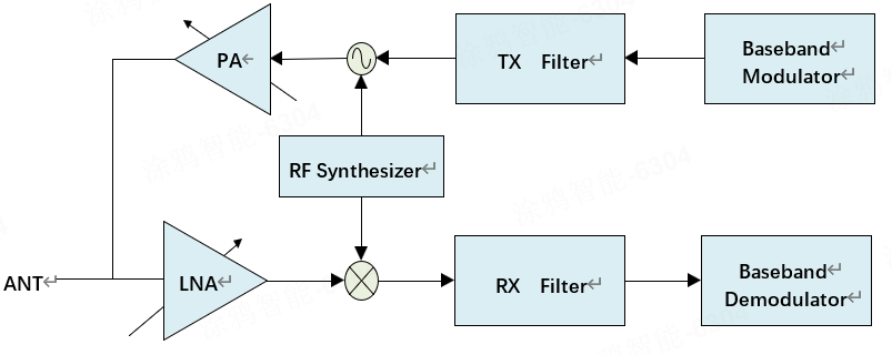
Bluetooth radio receiver
The OM6626 receiver is a low-IF down-conversion architecture. The RF signal passes first through an integrated transformer, which is shared between the receiver and transmitter. The transformer drives a differential variable-gain LNA, which amplifies the signal before it passes through a low-IF down-conversion mixer stage. Following the mixer is a third-order complex BPF, which performs channel selection and image rejection. The IF signal is then digitized by two SAR ADCs before further signal processing in the digital domain.
Bluetooth radio transmitter
The OM6626 transmitter is a direct modulating architecture. The digital baseband signals directly modulate the VCO and divider of the PLL, which is called two-point modulation. After a 3-stage class-D power amplifier, the radio signal is output through the antenna.
Frequency synthesizer
The OM6626 Frequency synthesizer is a fully integrated sigma-delta fractional-N PLL to lock the VCO to a reference crystal oscillator. The synthesizer uses several integrated linear regulators for better isolation of the blocks.
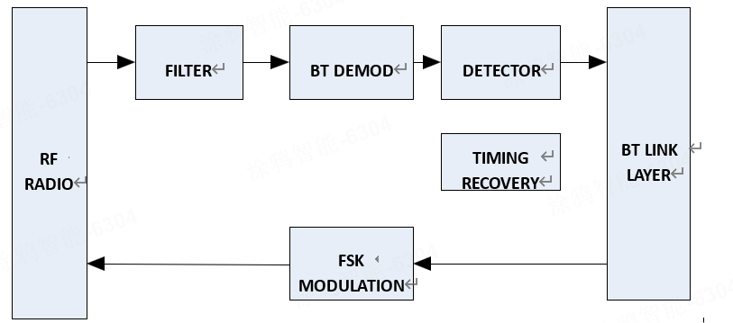
Bluetooth baseband unit
The BLE (Bluetooth Low Energy) core is a qualified Bluetooth 5.3 baseband controller compatible with Bluetooth Smart specification, and it includes packet encoding/ decoding and frame scheduling.
Main features
- All device classes support (Broadcaster, Central, Observer, Peripheral)
- All packet types (Advertising/Data/Control)
- Encryption (AES/CCM)
- Bit stream processing (CRC, Whitening)
- Frequency Hopping calculation
- Low power modes supporting 32.768 kHz
Performance
BLE receiver performance
[Supply voltage = 3.3V @ 25°C]
| Parameter | Min | Typ | Max | Unit | |
|---|---|---|---|---|---|
| Sensitivity, uncoded data at 1Ms/s | - | -98 | - | dBm | |
| Sensitivity, uncoded data at 2Ms/s | - | -95 | - | dBm | |
| Maximum received signal | - | 0 | - | dBm | |
| C/I co-channel Sensitivity, uncoded data at 1Ms/s | - | 6 | - | dB | |
| C/I co-channel Sensitivity, uncoded data at 2Ms/s | - | 6 | - | dB | |
| Adjacent channel selectivity C/I Note: F0=2440MHz | F = F0+1MHz, uncoded data at 1Ms/s | - | -5 | - | dB |
| F = F0 -1MHz, uncoded data at 1Ms/s | - | -4 | - | dB | |
| F = F0+2MHz, uncoded data at 1Ms/s | - | -42 | - | dB | |
| F = F0-2MHz, uncoded data at 1Ms/s (Image) | - | -32 | - | dB | |
| F = F0+3MHz, uncoded data at 1Ms/s | - | -52 | - | dB | |
| F = F0-3MHz, uncoded data at 1Ms/s | - | -48 | - | dB | |
| F = F0+2MHz, uncoded data at 2Ms/s | - | -8 | - | dB | |
| F = F0 -2MHz, uncoded data at 2Ms/s | - | -9 | - | dB | |
| F = F0+4MHz, uncoded data at 2Ms/s | - | -40 | - | dB | |
| F = F0-4MHz, uncoded data at 2Ms/s (Image) | - | -34 | - | dB | |
| F = F0+6MHz, uncoded data at 2Ms/s | - | -54 | - | dB | |
| F = F0-6MHz, uncoded data at 2Ms/s | - | -52 | - | dB | |
BLE transmitter performance
[Supply voltage = 3.3V @ 25℃]
| Parameter | Min | Typ | Max | Unit | |
|---|---|---|---|---|---|
| RF power control range | -30 | 0 | 8 | dBm | |
| ACP Note: F0=2440MHz |
F = F0±2MHz | - | -48 | - | dBm |
| F = F0±>3MHz | - | -50 | - | dBm | |
| ∆f1avg maximum modulation (uncoded data at 1Ms/s) | 225 | 250 | 275 | kHz | |
| ∆f1avg maximum modulation (uncoded data at 2Ms/s) | - | - | - | kHz | |
| ∆f2max maximum modulation | 185 | 200 | - | - | |
| (uncoded data at 1Ms/s) | |||||
| ∆f2max maximum modulation (uncoded data at 2Ms/s) | - | - | - | - | |
| ∆f2avg/∆f1avg (uncoded data at 1Ms/s) | 0.8 | 0.84 | - | - | |
| ∆f2avg/∆f1avg (uncoded data at 2Ms/s) | - | - | - | - | |
| Frequency Accuracy (uncoded data at 1Ms/s) | -150 | 7 | 150 | kHz | |
| Frequency Accuracy (uncoded data at 2Ms/s) | - | - | - | kHz | |
| Frequency Offset (uncoded data at 1Ms/s) | -150 | -7 | 150 | KHz | |
| Frequency Offset (uncoded data at 2Ms/s) | - | - | - | KHz | |
| Frequency Drift (uncoded data at 1Ms/s) | -50 | -12 | 50 | KHz | |
| Frequency Drift (uncoded data at 2Ms/s) | - | - | - | KHz | |
| Frequency Drift rate (uncoded data at 1Ms/s) | -20 | -10 | 20 | KHz/50us | |
| Frequency Drift rate (uncoded data at 2Ms/s) | - | - | - | KHz/50us | |
| Initial Frequency Drift (uncoded data at 1Ms/s) | -23 | -9 | 23 | KHz | |
| Initial Frequency Drift (uncoded data at 2Ms/s) | - | - | - | KHz | |
| 2nd harmonic distortion | - | -45 | - | dBm | |
| 3rd harmonic distortion | - | -50 | - | dBm | |
GPADC
Introduction
The OM6626 is equipped with a high-speed, low-power 12-bit general-purpose Analog-to-Digital Converter (GPADC). It can operate in unipolar (single-ended) mode.
Main feature
- 12-bit dynamic ADC with 3us conversion time
- Maximum sampling rate 333.3ksample/s
- Single-ended input
- 8x single-ended external input channels
- Battery monitoring function
- Temperature monitoring function
- Offset and gain calibration
- Support voltage input range: 0~VCC
Function description
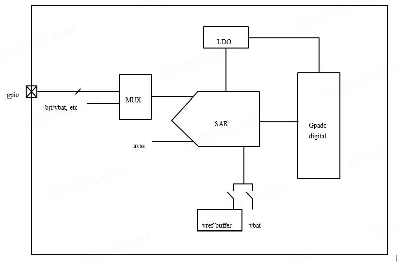
The analog MUX selects the input voltages to detect the temperature, supply voltage, and external voltage.
Electrical specification
| Symbol | Description | Min | Typ | Max | Unit |
|---|---|---|---|---|---|
| VAVDD | Main analog supply | 1.71 | - | 3.6 | V |
| VIN | Input range | 0 | - | VAVDD | - |
| IADC | Current consumption | - | 400 | - | uA |
| FSAMPLE | throughput rate | - | - | 333.3 | ksps |
| DNL | Differential non-linearity | - | - | - | LSB |
| INL | Integral non-linearity | - | - | - | LSB |
| ENOB | Effective number of bits | - | - | - | - |
| FSAMPLE=333.3ksps/256 | - | 11.9 | - | bits | - |
| FSAMPLE=333.3ksps/64 | - | 11.3 | - | bits | - |
| FSAMPLE=333.3ksps/8 | - | 10.8 | - | bits | - |
| FSAMPLE=333.3ksps | - | 9.6 | - | bits | - |
| SNDR | Signal to noise + distortion ratio | - | - | - | - |
| FSAMPLE=333.3ksps/256 | - | 73.4 | - | dB | - |
| FSAMPLE=333.3ksps/64 | - | 69.9 | - | dB | - |
| FSAMPLE=333.3ksps/8 | - | 66.7 | - | dB | - |
| FSAMPLE=333.3ksps | - | 59.3 | - | dB | - |
| VOS | Offset error (Calibrated) | - | - | - | - |
| GE | Gain error | - | - | - | % |
Package information
LGA28
The OM6626A has the LGA28 package. The information is as below:
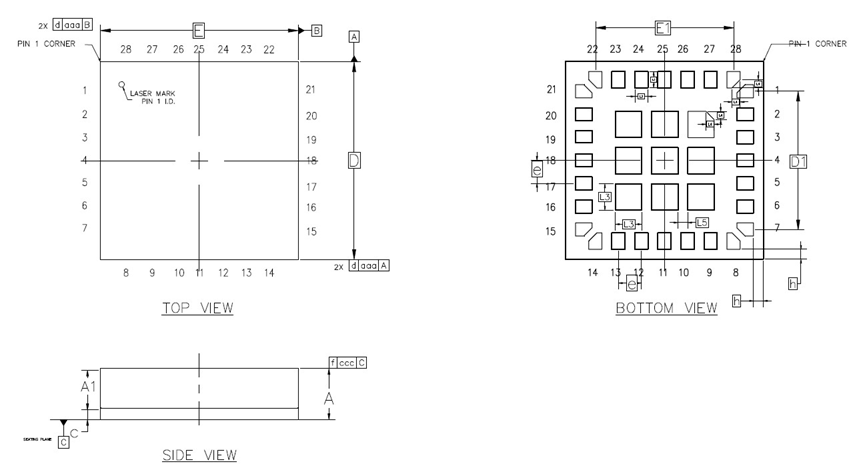
| Symbol | Millimeter | ||
|---|---|---|---|
| Min | Nom | Max | |
| A | 0.715 | 0.775 | 0.835 |
| A1 | 0.60 BASIC | ||
| c | 0.145 | 0.175 | 0.205 |
| D | 2.90 | 3.00 | 3.10 |
| D1 | 2.100 BASIC | ||
| E | 2.90 | 3.00 | 3.10 |
| E1 | 2.100 BASIC | ||
| e | 0.350 BASIC | ||
| L1 | 0.200 | 0.250 | 0.300 |
| L2 | 0.150 | 0.200 | 0.250 |
| L3 | 0.350 | 0.400 | 0.450 |
| L4 | 0.075 | 0.125 | 0.175 |
| L5 | 0.150 REF | ||
| h | 0.150 REF | ||
| aaa | 0.100 | ||
| ccc | 0.080 | ||
Note: The above dimensions are the design values of the factory’s process capability, excluding the raw edge dimensions.
QFN32
The OM6626B has the QFN32 package. The information is as below:
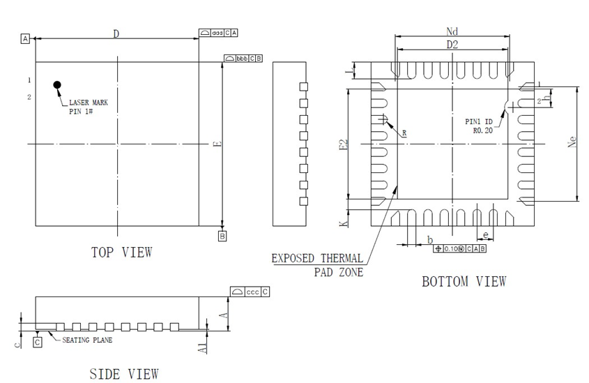
| Symbol | Millimeter | ||
|---|---|---|---|
| Min | Nom | Max | |
| A | 0.80 | 0.85 | 0.90 |
| A1 | 0 | 0.02 | 0.05 |
| b | 0.15 | 0.20 | 0.25 |
| c | 0.18 | 0.20 | 0.25 |
| D | 3.90 | 4.00 | 4.10 |
| D2 | 2.65 | 2.70 | 2.75 |
| e | 0.40BSC | ||
| Nd | 2.80BSC | ||
| K | 0.25Ref | ||
| E | 3.90 | 4.00 | 4.10 |
| E2 | 2.65 | 2.70 | 2.75 |
| Ne | 2.80BSC | ||
| L | 0.35 | 0.4 | 0.45 |
| h | 0.40 | 0.45 | 0.50 |
| R | 0.08 | 0.10 | 0.15 |
| aaa | 0.10 | ||
| bbb | 0.10 | ||
| ccc | 0.05 | ||
Note: The above dimensions are the design values of the factory’s process capability, excluding the raw edge dimensions.
Ordering information
OM6626 offers devices below for different application requirements.
| Part No. | Type | Package Size | Packing | MOQ (PCS) |
MPQ (PCS) |
Status |
|---|---|---|---|---|---|---|
| OM6626A | LGA-28L | 3*3mm 0.35mm Pitch | Tape/Reel | 3000 | 3000 | CS |
| OM6626B | QFN-32L | 4*4mm 0.4mm Pitch | Tape/Reel | 3000 | 3000 | CS |
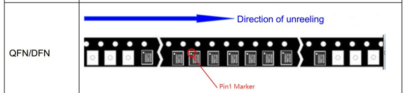
Tape and reel information
Tape orientation
General orientation of the OM6626x package in the carrier tape.
Tape and reel dimensions
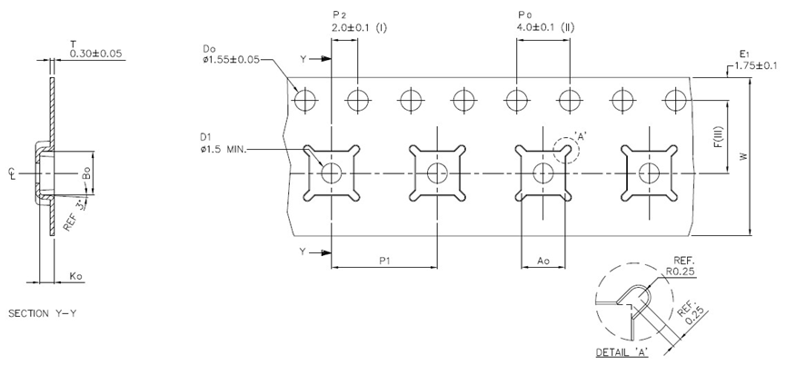
Common size:
| Appearance | Size / mm |
|---|---|
| E | 1.75 ± 0.10 |
| F | 5.50 ± 0.10 |
| P2 | 2.00 ± 0.10 |
| D0 | 1.55 ± 0.05 |
| D1 | 1.50 MIN. |
| P0 | 4.00 ± 0.10 |
| 10P0 | 40.00 ± 0.20 |
Bag size:
| Appearance | Size / mm |
|---|---|
| A0 | 3.30 ± 0.10 |
| B0 | 3.30 ± 0.10 |
| K0 | 1.10 ± 0.10 |
| P1 | 8.00 ± 0.10 |
| W | 12.00 ± 0.30 |
| T | 3.00 ± 0.05 |
OM6626B tape and reel dimensions
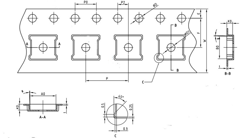
Common size:
| Appearance | Size / mm |
|---|---|
| E | 1.75 ± 0.10 |
| F | 5.50 ± 0.05 |
| P2 | 2.00 ± 0.10 |
| D | 1.55 ± 0.05 |
| D1 | 1.500+ 0.25 |
| P0 | 4.00 ± 0.10 |
| 10P0 | 40.00 ± 0.20 |
Bag size:
| Appearance | Size / mm |
|---|---|
| W | 12.00 ± 0.30 |
| P | 8.00 ± 0.10 |
| A0 | 4.30 ± 0.10 |
| B0 | 4.30 ± 0.10 |
| K0 | 1.10 ± 0.10 |
| t | 0.30 ± 0.05 |
| θ | 3°TYP |
Glossary and abbreviations
| Name | Description |
|---|---|
| ADC | Analog to Digital Converter |
| AGC | Automatic Gain Control |
| AON | Always-on |
| APB | Advanced Peripheral Bus |
| BB | Base band |
| BLE | Bluetooth Low Energy |
| BOD | Brown-out Detector |
| IFS | Inter Frame Spacing |
| LDO | Low Dropout |
| LNA | Low Noise Amplifier |
| LPD | Low Power Domain |
| NVM | Non-volatile memory |
| PLL | Phase Locked Loop |
| PMU | Power Management Unit |
| RNG | RING Oscillator |
| SOC | System-on-chip |
| TPMS | Tire pressure monitor system |
| W1C | Write 1 to clear |
| XO | Crystal Oscillator |
| Typ | Typical |
| SNR | Signal to Noise Ratio |
| PA | Power Amplifier |
| IRQ | Interrupt Request |
| LSB | Least Significant Bit |
| MSB | Most Significant Bit |
| DFE | Digital Front End |
Declaration of no harmful substances
This part is compliant with 2005/20/EC packaging directive, 1907/ 2006/ EC REACH directive, and the 2011/65/EU RoHS directive (Restrictions on the Use of Certain Hazardous Substances in Electrical and Electronic Equipment), as amended by Directive 2015/863/EU.

This product also has the following attributes:
- Lead free
- Halogen Free (Chlorine, Bromine)
- SVHC Free
Is this page helpful?
YesFeedbackIs this page helpful?
YesFeedback


