Hardware Design Reference
This topic describes hardware design for keep-alive Wi-Fi locks. The keep-alive Wi-Fi solution can be used to create persistent connections with ultra-low power consumption. This solution can minimize the power consumption that is measured in µA when devices are in sleep mode. In this solution, the module consists of a highly-integrated radio frequency (RF) processor chip, an external microcontroller unit (MCU), and a few peripheral components. This solution supports printed circuit board (PCB) antennas and IPEX antennas and enables comprehensive wireless connections over multiple protocols. Serial communication is supported to implement data transmission with the MCUs in other services.
Hardware design
The keep-alive Wi-Fi no-code development solution is implemented based on the HPWSMS1 module provided by Tuya. For more information, see HPWSMS1 Module Datasheet. This module supports the following types of antennas:
- PCB antenna: For more information about the antenna design, see the inverted-F antenna diagrams in the Structural design section.
- IPEX antenna: You can build a model of this type of antenna based on a specific product structure.
Schematic diagrams
-
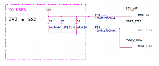
Power supply design: The working voltage of the power supply circuit is 3.3V. The Wi-Fi chip is powered separately from RTL8762. The magnetic beads FB1 and FB2 are reserved as current test points.
-
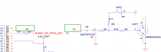
The antenna design for the Wi-Fi module HPWSMS1 must follow these rules:
-
The 3.3V_Wi-Fi power pin in the preceding figure is connected to a filter capacitor.
-
Each of the pins 49, 29, 82, and 94 is connected to a separate 1 μF/10V filter capacitor.
-
The pin 98 is connected to a 10 μF/10V filter capacitor.
-
The pin 78 is connected to a 0.1 μF/16V filter capacitor.
-
The module supports the following pins:
HOST_BYP_ULP_WAKEUP,SLEEP_IND_FROM_DEV,ULP_GPIO_6, ULP_GPIO_5, andRESET_N. Each pin is connected to a resistor in series and then to a specific pin of RTL8762 to enable the required function. -
The pins
WIFI_UART1_RXandWIFI_UART1_TXare used for communication between the Wi-Fi module and RTL8762. Test points must be reserved for connection to a flashing tool.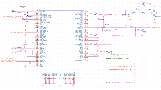
-
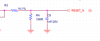
A 10 mR pull-down resistor is used to process the RESET_N signal. The following figure shows the specific design.
-
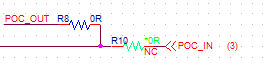
The pin 92 POC_OUT and the pin 65 POC_IN are connected through 0R. POC_IN is reserved for connection to the NC resistor R10 to process control signals of RTL8762.
-
The RF channel is only connected to the pin 32. The impedance matching must be 50 Ω in the layout design. A PCB antenna or an IPEX antenna can be used to meet your product requirements.
-
-
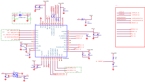
The design of the RTL8762 development board follows these rules:
- Recommended crystal oscillator specifications: 40 MHz—±10 ppm—9 pF—-30°C–+85°C—SX3225—surface-mount technology (SMT). The frequency deviation is at most 10 ppm. The integrated circuit is packaged. Recommended cyrstal specifications: 32.768 kHz—20 ppm—7 pF—SMD2012.
- A capacitor of at least 0.1 μF X5R 6.3V is connected to the power pin of VDD12. We recommend that you connect the capacitor in the same way as that shown in the preceding diagram.
- L2 is a power inductor with the following specifications: rated current > 0.5A, DC resistance (DCR) < 1 Ω, self resonant frequency (SRF) > 40 MHz.
- Recommended C15 specifications: 2.2 μF, X5R, and 10V.
- The voltage for each of VBAT_8762 and VDDIO_8762 reaches 3.3V.
- Each of the pins 39 and 21 is a combination of the 1 μF/6.3V and 0.1 μF/6.3V filter capacitors.
- The pin 32 is the 4.7 μF/6.3V filter capacitor.
- The RESET signal is pulled up to VBAT_8762 with a 10 kΩ resistor.
- Test points must be reserved for the following signals to implement debugging and production testing:
- P0_3: used to view logs.
- UART2_TX/UART2_RX: used for firmware flashing and updates.
- SWDCLK/SWDIO: used for Joint Test Action Group (JTAG) debugging.
- 3V3 and GND: Test points are reserved for debugging.
PCB design reference
-
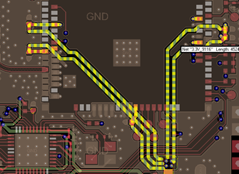
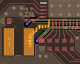
The 3.3V_WIFI power supply of the HPWSMS1 is deployed in a star network. The trace width must be at least 20 mil.
-
The L2 inductor of RTL8762 is placed close to the chip pin to minimize the inductive loop.
-
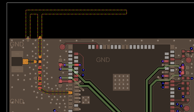
Ground vias are added around the RF channel. The 50 Ω impedance matching is provided.
-
The test points can be easily reached by the test jig. The output signals of the test points include 3.3V, GND, P0_3, WIFI_UART1_TX, WIFI_UART1_RX, UART2_TX, UART2_RX, SWDCLK, and SWDIO.
Structural design
When you design a product ID, you must determine the antenna location first. You can select a PCB antenna or an IPEX antenna.
Note: We recommend that you confirm the antenna location and things to note with the antenna manufacturer at the beginning of the structural design.
Usage of PCB antennas
-
When a PCB antenna is used, we recommend that the module antenna is at least 15 mm away from other metal components. This can optimize the Wi-Fi performance. Traces and copper pour areas are not allowed in the antenna area of the PCB. Otherwise, antenna performance might be reduced.
-
The final performance features of the PCB antenna depend on multiple factors, such as the product structure, materials, and module location, and the dimensions and shape of the backplane. The performance of the entire product is subject to actual testing.
-
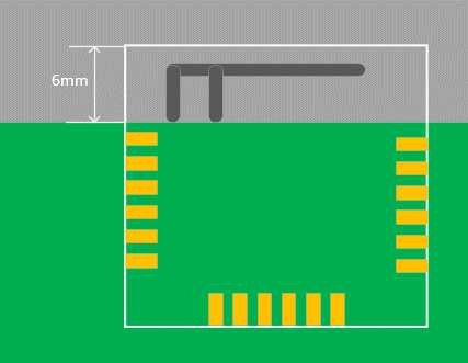
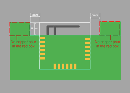
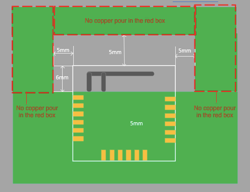
You can use a PCB antenna for the module in specific structural conditions. For example, the PCB antenna can be attached to the non-metal shell of the whole device, or a sufficient clearance area is reserved. The following three figures show the recommended PCB layouts with the antenna. Make sure that a substrate medium does not exist below the antenna. A copper pour area is not found around the antenna to minimize the impact on the antenna performance. If located too close to the antenna, copper foil might affect the resonance point of the antenna, or the substrate medium might reduce the radiation efficiency of the antenna. To solve this issue, the following first figure shows the recommended location of the PCB antenna.
-
The antenna is located outside the backplane frame.
-
The antenna is located along the backplane frame. No copper pour area is allowed inside the frame.
-
The antenna is located along the midline of the backplane. The backplane frames around the antenna are hollowed out.
-
Based on the preceding PCB layout solutions, no substrate medium or metal part of the whole device exists directly below or directly above the PCB antenna. The PCB antenna is away from the copper sheet. This can maximize the radiation effect of the antenna.
Usage of IPEX antennas
-
An IPEX antenna is an ideal option for a Wi-Fi module that is used by the whole device. Put the antenna at the optimal position away from the interference of metal parts.
-
To fix a flexible printed circuit (FPC) antenna, you can stick the antenna on a non-metal shell or use an antenna bracket.
-
The placement of the IPEX antenna depends on the design and structure of the whole device. Evaluate the location of the antenna and debug the RF performance based on the actual structural design. This allows you to conform to different certifications and regulations. The module can determine the RF performance on the backplane, but cannot cover the overall performance of different forms.
-
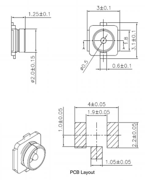
The following figure shows the recommended specifications of the IPEX connector.
-
Other layout rules:
- Keep a distance of 3 cm or more between the module and speakers, power switches, cameras, High-Definition Multimedia Interface (HDMI) connectors, USB connectors, and other high-speed signals to avoid interference.
- Reserve a sufficient clearance area below the antenna. No wiring or other medium layer is allowed in this clearance area to avoid interference from structural parts.
- Avoid metal shielding near the antenna. If co-channel interference occurs, you must evaluate the impact on the antenna and ensure the isolation from the interference.
- The antenna radiation directions cannot be blocked by metal.
Bill of materials
| Item code | Item description | Manufacturer | Manufacturer-managed model | Quantity | Position |
|---|---|---|---|---|---|
| 1.14.99.00020 | Other connectors, IPEX antenna mount, UB06000004A, 2 mm outer ring and 0.5 mm inner pin, gold-plated phosphor bronze, -40°C–+90°C, and SMT | Ubuant | UB06000004A | 1 | ANT1 |
| 2.06.03.01057 | Material combination, ceramic capacitor, SMT, X5R, 10 μF, ±10%, 16V, and 0805 | Capacitor | 201 | 1 | C1 |
| 2.06.03.01148 | Material combination, ceramic capacitor, SMT, X5R, 1 μF, ±20%, 6.3V, and 0201 | Capacitor | 292 | 8 | C2, C10, C16, C17, C19, C22, C24, and C32 |
| 2.06.03.00857 | Material combination, ceramic capacitor, SMT, X5R, 0.1 μF, ±10%, 6.3V, and 0201 | Capacitor | 001 | 7 | C3, C11, C18, C20, C21, C23, and C25 |
| 2.06.03.01150 | Material combination, ceramic capacitor, SMT, X5R, 10 μF, ±20%, 10V, and 0402 | Capacitor | 294 | 1 | C4 |
| 2.06.03.01154 | Material combination, ceramic capacitor, SMT, X5R, 1 μF;±10%, 10V, and 0402 | Capacitor | 298 | 3 | C5, C6, and C29 |
| 2.06.03.01031 | Material combination, ceramic capacitor, SMT, C0G, 22 pF, ±5%, 50V, and 0402 | Capacitor | 175 | 1 | C8 |
| 2.06.03.01145 | Material combination, ceramic capacitor, SMT, X5R, 4.7 μF, ±20%, 6.3V, and 0402 | Capacitor | 289 | 1 | C12 |
| 2.06.03.00972 | Material combination, ceramic capacitor, SMT, X5R, 2.2 μF, ±10%, 10V, and 0402 | Capacitor | 116 | 1 | C15 |
| 2.06.03.01136 | Material combination, ceramic capacitor, SMT, C0G, 12 pF, ±5%, 50V, and 0201 | Capacitor | 280 | 2 | C26 and C27 |
| 1.04.03.00007 | Magnetic bead, 180R@100 MHz, 0.09R, 1.5A, 0603, and SMT | Sunlord | PZ1608D181-1R5TF | 1 | FB1 |
| 1.04.03.00009 | Magnetic bead, 120R@100 MHz, 0.12R, 1A, 0402, and SMT | Sunlord | PZ1005U121-1R0T | 1 | FB2 |
| 1.04.02.00625 | Power inductor, 4.7 μH, 0.2, 0.125R, 1.09A, 3.0 × 3.0 × 1.5 mm, and SMT** | Sunlord | SWPA3015S4R7MT | 1 | L2 |
| 2.06.03.00028 | Material combination, SMD resistor, 0402, 0R, ±5%, and 1/16W | SMD resistor | 4355 | 13 | R1 R2 R5 R7 R8 R9 R11 R12 R13 R14 R16 L1 |
| 2.06.03.00032 | Material combination, generic resistor, 1K, ±1%, 0402, 1/16W, and SMT | Generic resistor | 4361 | 1 | R3 |
| 2.06.03.00733 | Material combination, generic resistor, 10M, ±5%, 0201, 1/20W, and SMT | Resistor | 688 | 1 | R4 |
| 2.06.03.00047 | Material combination, generic resistor, 10K, ±5%, 0402, 1/16W, SMT, and 50V | Resistor | 002 | 1 | R15 |
| 1.17.13.00587 | RF transceiver IC, Bluetooth, -40°C–+105°C, QFN40, and SMT | Realtek | RTL8762CMF | 1 | U2 |
| 2.01.01.102735 | General Wi-Fi module, Wi-Fi and Bluetooth Low Energy, HPWSMS1, RS9116, and external antenna (welded to the backplane without an IPEX mount, the antenna mount placed on the backplane) | Tuya | HPWSMS1 | 1 | U1 |
| 2.06.03.00859 | Material combination, ceramic capacitor, SMT, X7R, 0.1 μF, ±10%, 16V, and 0402 | Capacitor | 003 | 1 | C7 and C28 |
| 2.06.03.00981 | Material combination, ceramic capacitor, SMT, X5R, 1 nF, ±10%, 25V, and 0201 | Capacitor | 125 | 1 | C9 |
| 1.03.02.00724 | Crystal oscillator, 32.768 kHz, ±20 ppm, 7 pF, 65K, -40°C–+85°C, 2012, and SMT | EPSON | X1A0000610006xx | 1 | Y1 |
| 1.03.02.00762 | Crystal oscillator, 40 MHz, ±10 ppm, 15 pF, 30R, -40°C–+85°C, ±20 ppm, 3225, and SMT | Faith Long | 3S40000066 | 1 | Y2 |
| 1.21.05.00764 | PCB substrate, S-MSL1-S-HX-001_V1.0.0, 36 × 36 × 1.2 mm, 4L, electroless nickel immersion gold (ENIG), green and white, plated half holes, and halogenated** | 1 | |||
| 1.02.99.00026 | Ceramic capacitor, SMT, X5R, 1 nF, ±10%, 25V, and 0201 | Murata | GRM033R71E102KA01D | 1 | C9 |
| 1.02.05.00842 | Ceramic capacitor, SMT, X7R, 1 nF, ±10%, 25V, and 0201 | Walsin | 0201B102K250CT | / | / |
| 1.02.05.00837 | Ceramic capacitor, SMT, X7R, 1 nF, ±10%, 25V, and 0201 | Yageo | CC0201KRX7R8BB102 | / | / |
| 1.03.02.00724 | Crystal oscillator, 32.768 kHz, ±20 ppm, 7 pF, 65K, -40°C–+85°C, 2012, and SMT | EPSON | X1A0000610006xx | / | / |
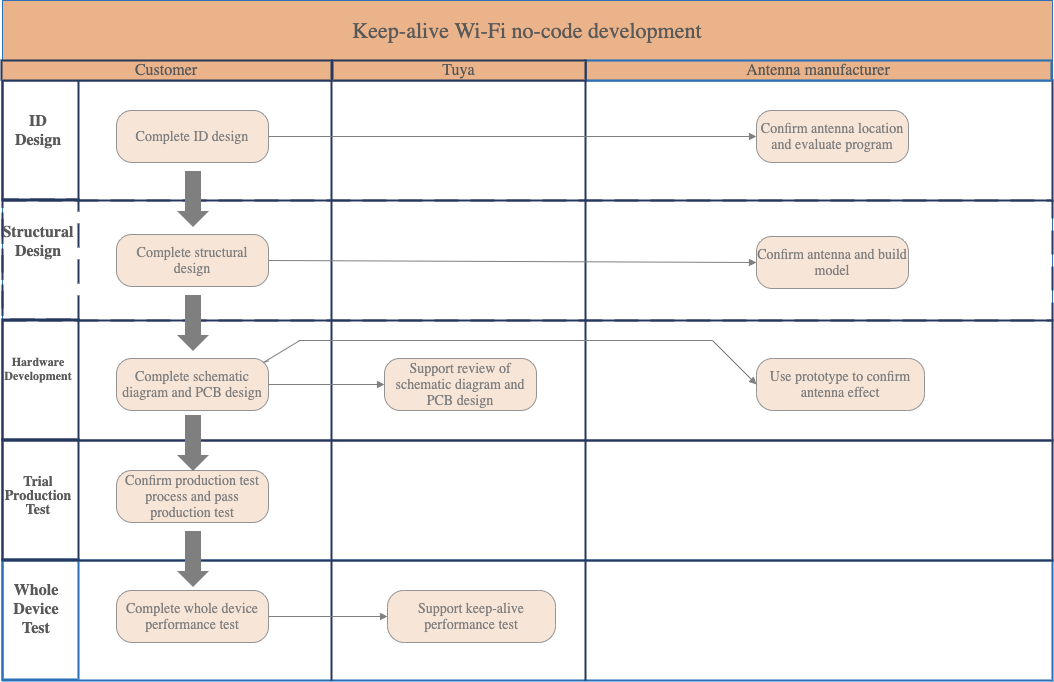
Solution process
Is this page helpful?
YesFeedbackIs this page helpful?
YesFeedback


