Application and Layout of Limited Module
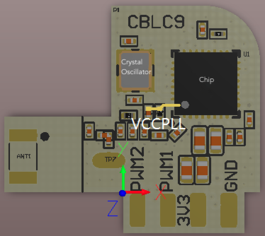
Sensitive components inside wireless modules include chips, crystal oscillators, and internal power supplies, such as the VCCPLL power supply of the 7231N chip. Once these sensitive components and traces are interfered with, their transmitting and receiving performance will be affected. Tuya’s Wi-Fi, Bluetooth, and Zigbee modules without shielding covers, such as CBLC5, CBLC9, ZTLC5, BTLC5, and BPLCB, have internal sensitive components that are more susceptible to interference.
When modules are used in LED lighting products, the power supply for the LED driver generally adopts a switching power supply solution, whether they are powered by the modules or the main power supply. There are switching power devices in the switching power supply solution, such as MOSFETs, power inductors, and flyback diodes. When the switching device is operating, radiation interference is generated. An improper PCB layout can greatly compromise the RF performance of the module, leading to pairing and connection exceptions, shortened control distance, and other problems.
There are generally two types of switching power supply solutions for LED driver: AC-DC power supply and DC-DC power supply.
How AC-DC power supplies work
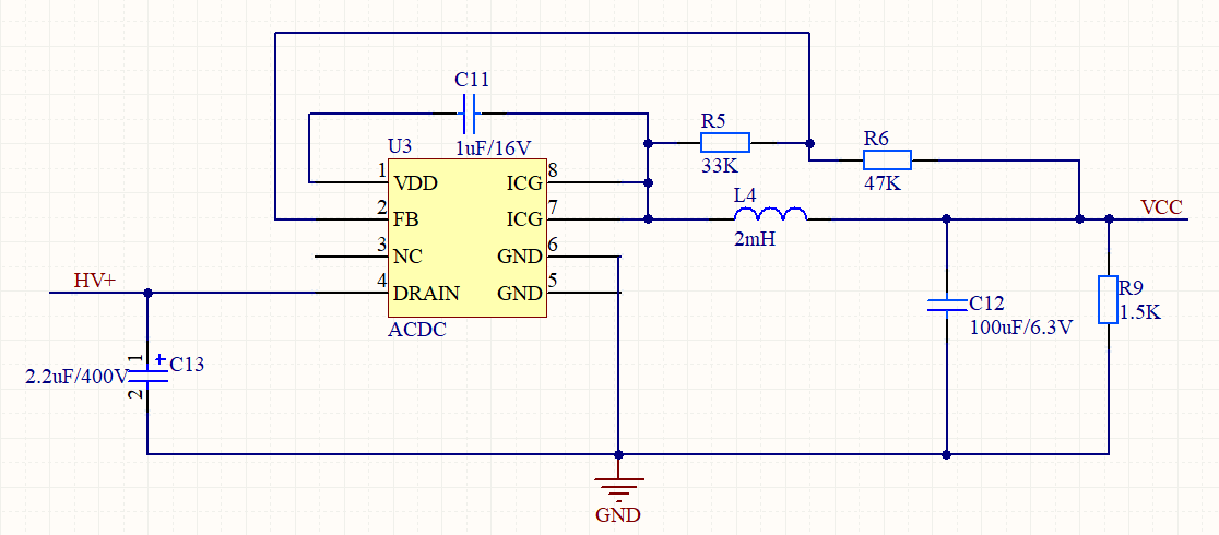
In the above solution, the AC-DC chip has built-in power MOSFET and flyback diode, and the peripheral switching power device is the inductor L4. L4 can use I-shaped inductors, E-shaped inductors, and SMD inductors.
For the design of an AC-DC switching power supply solution, pay attention to the following points:
-
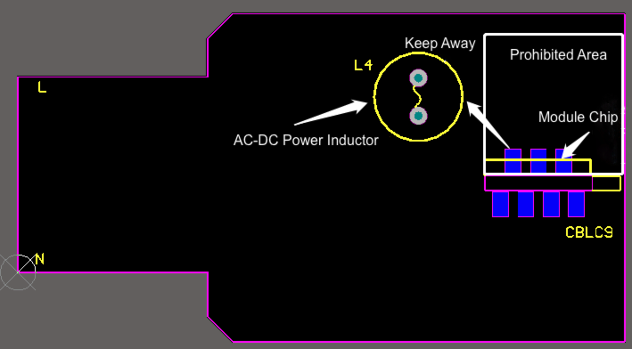
The power supply for the LED driver has a large space in light source solutions A, B, BR, MR, PAR, GU10, and C37. Try to keep the inductor L4 away from the side of the module with the chip. The inductor L4 cannot be placed in the area directly in front of the module and should be as far away from the direction of the module chip as possible. Refer to the diagram below.
-
LED driver space is limited. For example, small lamp sockets E26 and E14d have built-in LED driver power supplies, and generally use unshielded modules such as LC5 and LCB.
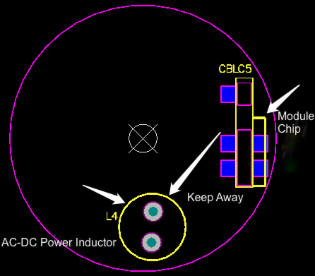
Taking the LED driver power supply of the E26 filament lamp socket in the image above as an example, the module is placed with the chip facing the outside as much as possible, and the power inductor is kept away from the module. For AC-DC power inductors, EE-shaped inductors are preferred to I-shaped inductors. Make sure the inductor is not saturated under application conditions.
If SMD inductors are used, glue-shielded or magnetic-shielded inductors are recommended to reduce the interference of inductor radiation on the chip.
How DC-DC power supplies work
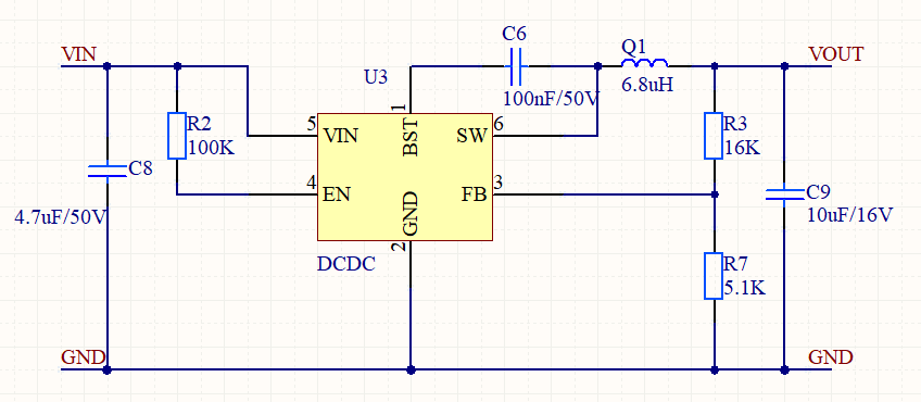
Taking the DC-DC step-down switching power supply as an example, the basic principle is shown as above. Power inductor Q1 can be SMD inductors, I-shaped inductors, and E-shaped inductors. For DC-DC step-down power supplies, the inductor should be away from the module chip and away from the RF traces. For example, the white highlight in the figure below is the RF traces.
In order to reduce the interference of high-frequency signals, choose glue-shielded or magnetic-shielded inductors, and make sure the height of the inductor is not greater than that of the module.
-
Based on the above analysis, in specific circuit applications, module chips and crystal oscillators should be kept away from AC-DC inductors, DC-DC inductors, LED driver chips, and other mains-powered devices with a certain switching frequency.
-
In addition, try not to face the switching device directly against the chips and crystal oscillators, especially for limited modules without shielding covers. Place these interference-causing mains-powered devices on the back of the module to reduce coupling interference to the front of the module chip and crystal oscillator.
-
If necessary, verify the RF performance under the working condition of the complete PCBA before mass production. For example, distance test and pairing test.
Example
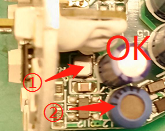
In the figure below, mark 1 is a DC-DC inductor, which is low in height and not facing the module. Therefore, the design is relatively appropriate. Mark 2 is an AC-DC inductor, which is far away from the module, not facing the module, and is blocked by capacitor space. Therefore, the design is appropriate.
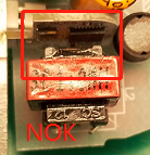
In the figure below, the magnetic leakage port of the AC-DC inductor is facing the module chip and is almost adjacent to it. Therefore, the design is inappropriate.
-
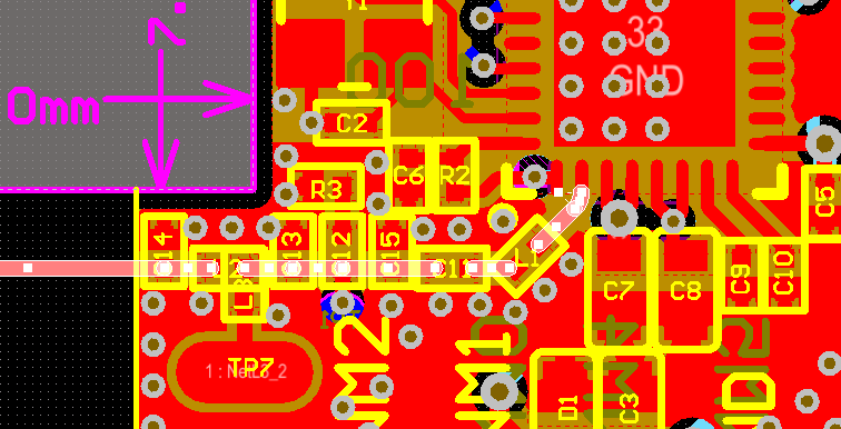
For 2S form factor modules (such as models ZT2S, T1-M, T3-M, T1-2S, etc.) when connecting to the customer’s baseboard, ensure an adequate antenna keep-out area. For example, within 6mm of the antenna, avoid placing components like electrolytic capacitors and power inductors as much as possible. Otherwise, the low-frequency components generated by these components during operation may interfere with the module’s antenna reception.
-
All pin pads of the module should be fully soldered to the baseboard. Even if some I/O ports are not used, they should still be soldered to the baseboard to improve the grounding effect between the module and the baseboard.
-
The ground plane on the customer’s baseboard should be widened as much as possible. Avoid using long, single-trace GND routing, as this can lead to poor grounding performance for the module.
Is this page helpful?
YesFeedbackIs this page helpful?
YesFeedback


