Precautions for Product RF Design
Overview
Tuya wireless modules are used in lighting, and the position of the modules needs to be arranged reasonably, and the clear space around the antenna is reasonably ensured to ensure the full play of the wireless performance. Generally, there are two ways to connect the module and the LED driver baseboard: ①Connect to the PCB baseboard by SMT welding. ②It is soldered on the PCB backplane by means of a plug-in. At the same time, there are usually two antenna forms of the module: ①The module comes with a PCB-printed antenna. ②The module adopts an external soft antenna or spring antenna. The following documents give a reasonable layout and antenna layout guidelines for each situation.
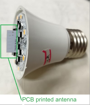
The main points of the layout of the plug-in module of the printed antenna
The plug-in module is connected to the control board through the upper pin or plug-in pad. Since the base of the bulb and the surrounding shell is made of metal, including the aluminum substrate where the lamp beads are located, wireless signals cannot penetrate these metal materials. It is necessary to ensure that the printed antenna can penetrate the aluminum substrate and maintain a certain height. On the premise of not affecting the quality of light source projection, the closer the antenna is to the bulb front area, the more conducive to signal penetration and emission. In Figure 1, the green frame shows the printed antenna. In the actual layout, try to keep clear space near the antenna, especially something like metal pin headers. Keep a distance of more than 6mm.
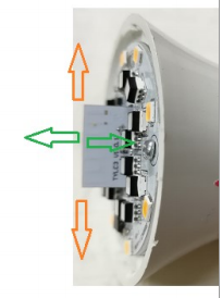
The above figure 3 indicates that the green arrow represents the direction of the strongest radiation of the printed antenna; the orange arrow represents the direction of the relatively weakest radiation of the printed antenna. The above figure can be used as a reference for evaluation when the customer is in the actual module layout. At the same time, the module’s crystal, RF Soc, and other core components should be kept away from the heating components in the driver backplane, light source area as much as possible to avoid excessive local temperature rise and cause the surface temperature of the core components to exceed 105 °C.
Layout considerations for SMD modules
Make sure that a substrate medium does not exist below the antenna. A copper pour area is not found around the antenna to minimize the impact on the antenna performance. If located too close to the antenna, copper foil might affect the resonance point of the antenna, or the substrate medium might reduce the radiation efficiency of the antenna.
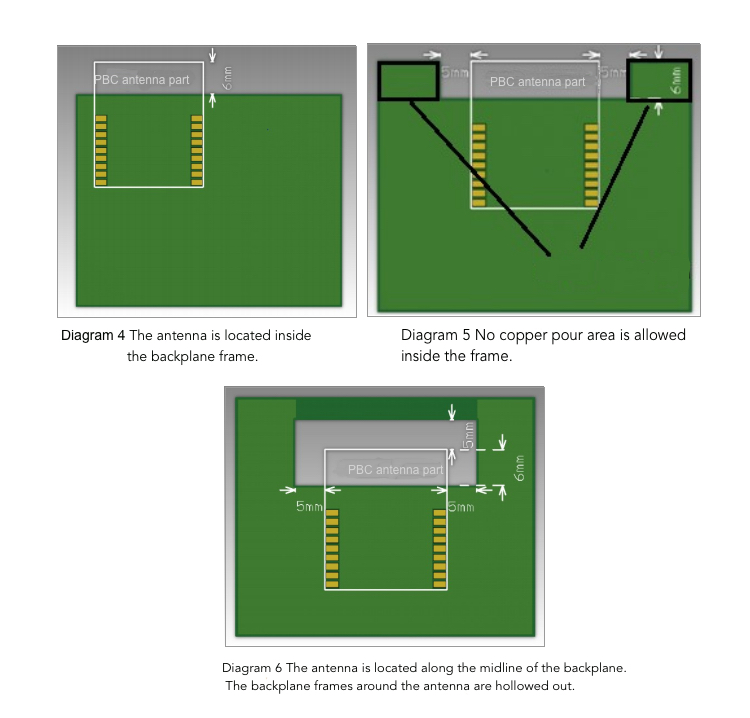
Based on the preceding PCB layout solutions, make sure that no substrate medium exists directly below or above the printed antenna, and the printed antenna is away from the copper sheet. In this way, the antenna radiation effect is guaranteed to the maximum extent.
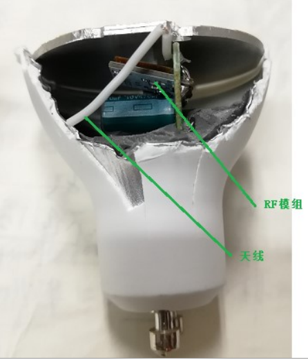
Module with external antenna scenario
For scenes with external antennas, the antenna should be as far away from the base and aluminum substrate as possible without affecting the projection of the light source. For example, use a monopole soft antenna or a monopole spring antenna to go deep into the inner vertical column part of the filament lamp. See Figure 7 below, examples of spring antennas and soft antennas:
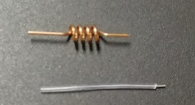
Figure 7 Spring antenna & soft antenna
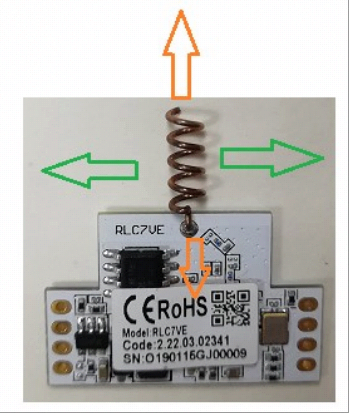
Figure 8 Schematic diagram of the radiation effect of the external antenna of the module
Figure 8 above shows a module with an external antenna. The module antenna is generally perpendicular to the area above the aluminum substrate. The orange arrow indicates the direction of relatively weak radiation, and the green arrow indicates the direction of relatively strong radiation. Note that there should be no metal parts around the copper pillar antenna. Metal will greatly hinder the transmission of wireless signals. Make sure that the copper pillar antenna is as far away from the lampshade in the center as possible, and the vertical height of the metal ring on the lampshade should not exceed the antenna. Figure 9 below shows an improper layout. The antenna of the module is completely blocked under the aluminum substrate, causing the wireless signal to not radiate, which ultimately affects the connection quality of the whole machine to a large extent.
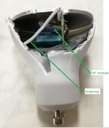
Figure 9 Inappropriate layout
If there is a structural difficulty in directly soldering the antenna to the pin of the module, you can add an exposed pad to the adapter board. The size of the pad is recommended to not exceed 2 × 3mm. Then solder the soft antenna to the pad to ensure that the antenna can go deep. To the front end of the lamp body. The details are shown in Figure 10 below. The purpose of selecting the soft antenna is to adapt the structure of the lamp body through relatively random bending, but it is necessary to ensure that there are no metal parts around the soft antenna as much as possible, and the length of the soft antenna is deep into the front end of the lamp body is sufficient.
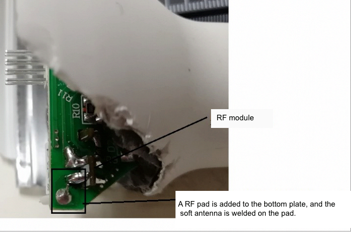
Figure 10 Adding RF pads on the bottom board
Is this page helpful?
YesFeedbackIs this page helpful?
YesFeedback


