TYBN1 Module
This topic describes Tuya’s proprietary low-power TYBN1 Bluetooth module.
Features
The TYBN1 consists of a highly integrated nRF52832 Bluetooth chip and a few peripheral circuits. It has built-in Bluetooth protocol stacks and a rich set of library functions.
The TYBN1 is built around a 32-bit Arm Cortex-M4 MCU with 512 KB flash and 64 KB SRAM. It has 11 GPIOs and 4-channel ADC. The embedded 2.4 GHz transceiver supports Bluetooth low energy.
For more information, see TYBN1 Module Datasheet.
Typical application circuit
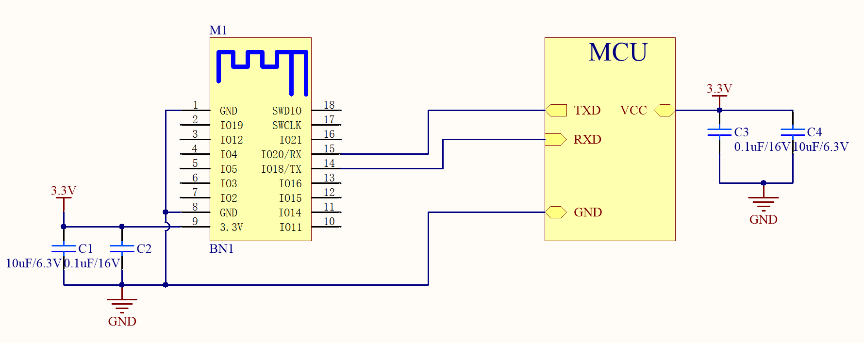
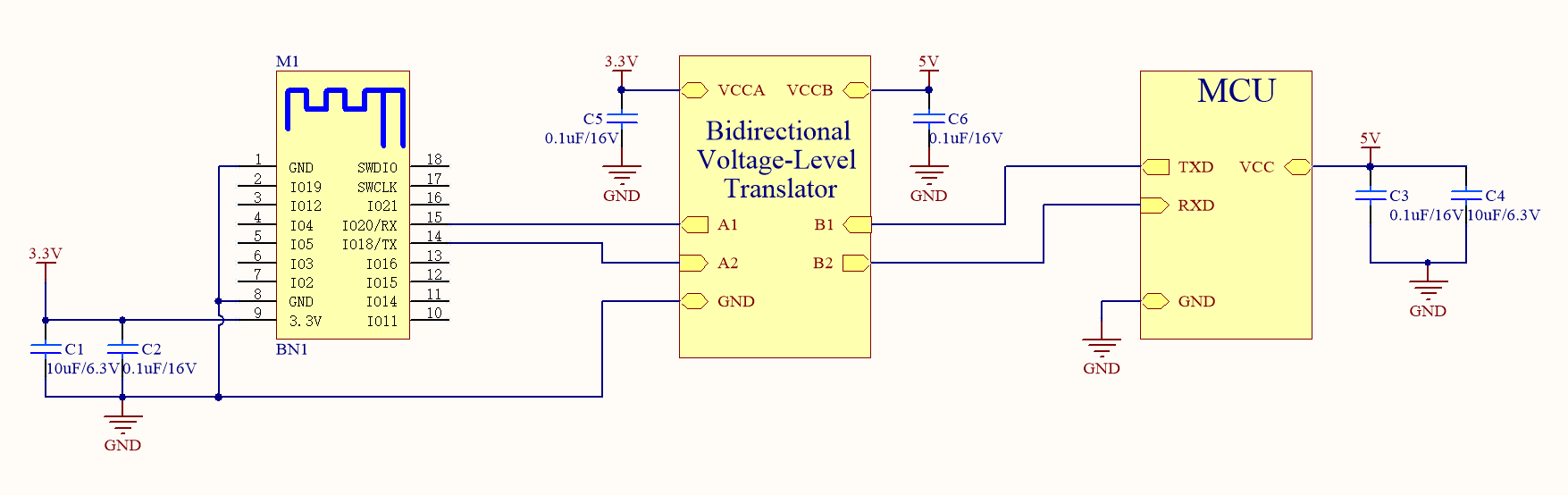
Generic solution
-
Connection between a module and a 3.3V MCU
-
Connection between a module and a 5V MCU
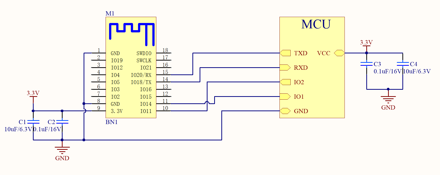
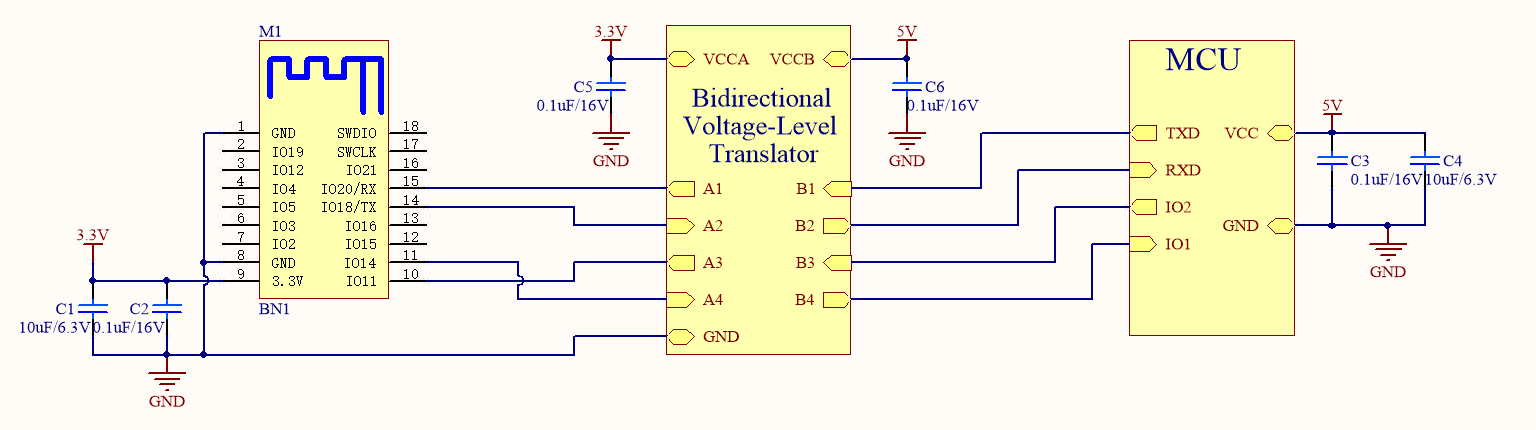
Low power solution
-
Connection between a module and a 3.3V MCU
-
Connection between a module and a 5V MCU
Level translator reference
-
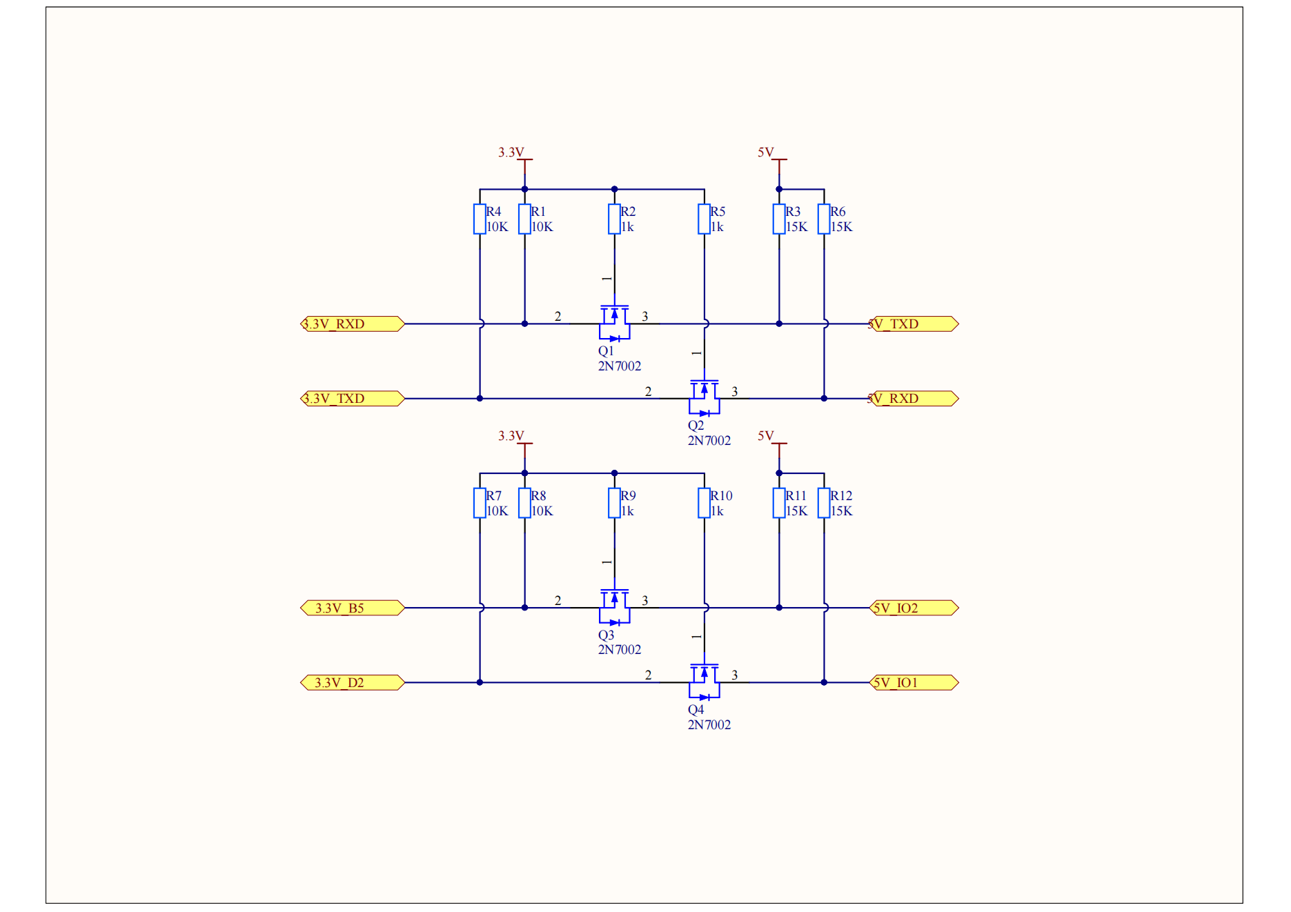
N-channel MOSFET level translator
In the following circuit diagram, an N-channel MOSFET and a built-in body diode are used to implement two-way communication.
-
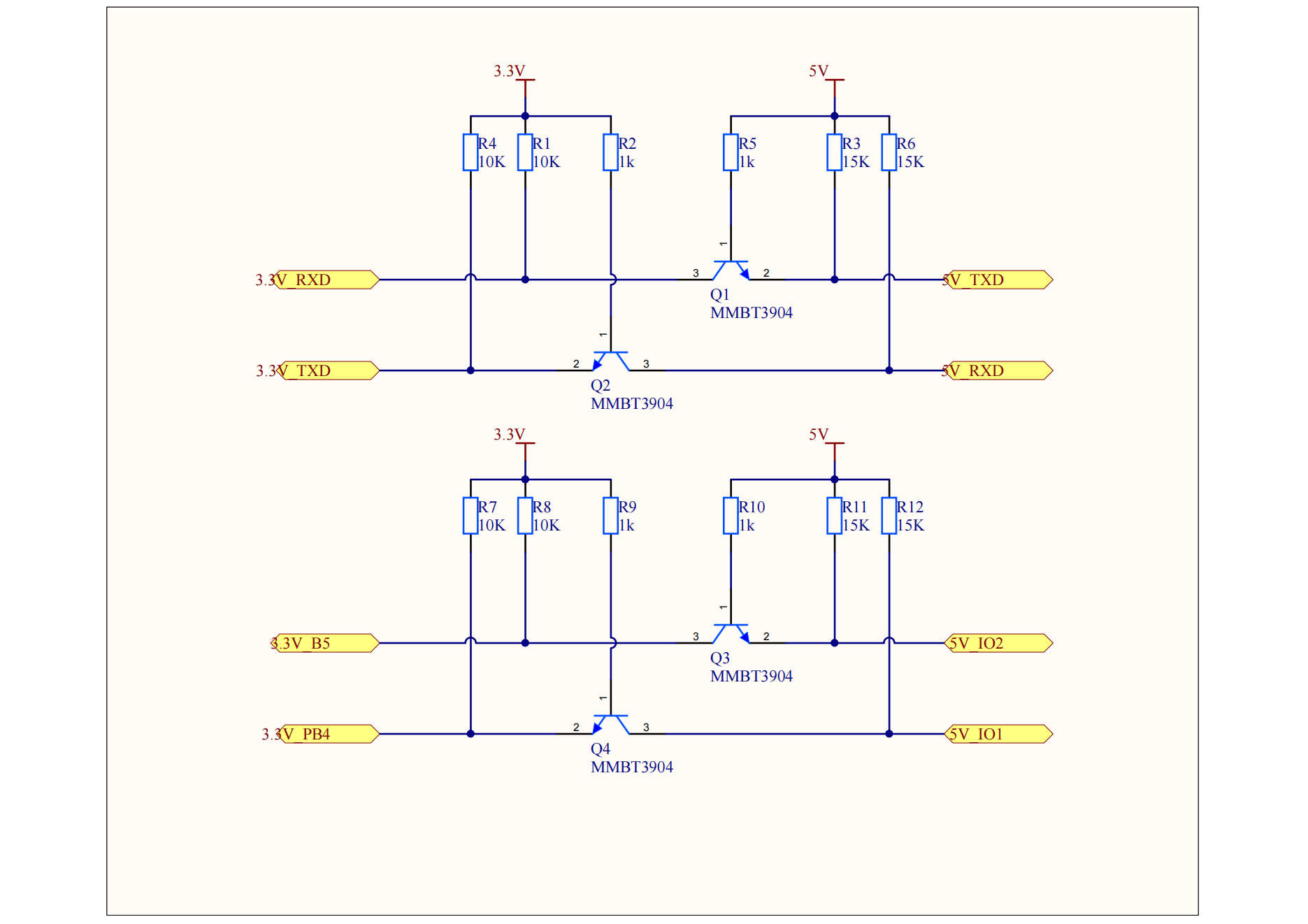
NPN triode level translator
In the following circuit diagram, an NPN triode is used to implement one-way communication.
For more information, see Bluetooth Serial Communication Protocol.
Design specification
-
Power supply
- The supply current for 3.3V modules should be greater than 100 mA. The total capacity of the external filter capacitor should be greater than 10 μF.
- Place the filter capacitors of the power input pin near the power pin of the module.
-
Pins of the module
-
The module has a power-on-reset circuit. You can also use the GPIO on the MCU to control the module reset. Take care of the voltage level translation.
-
The MCU can pull down or up the low power pin on the module to make the module enter or exit the sleep mode. The configuration is shown below.
Low power pin Voltage level in low power Voltage level in standard power I/O 11 High Low -
The module can change the level of the wake-up pin for 200 milliseconds to wake up the MCU for serial data transmission. After that, the pin will go back to the default level. The configuration is shown below.
Wake-up pin Voltage level on transmitting Voltage level on idle I/O 14 Low High
-
-
Radio frequency
The distance between the antenna and other mental components should be at least 15 mm to provide the best RF performance.
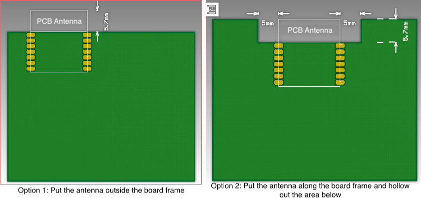
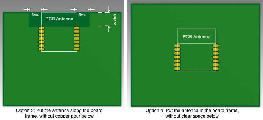
The TYBN1 is assembled by SMT. The antenna design and RF layout directly determine the RF performance. The following four figures present four RF layouts. We take a look at their advantages and disadvantages.
-
Option 1 and 2 are recommended. Place the antenna outside the border, or cut out the area around the antenna. Basically, these two options do not compromise the RF performance.
-
If your circuit design requires antenna placement on the backplane, refer to option 3. Place the antenna inside the border but do not fill copper or route trace around the antenna. This option compromises the RF performance by 1 to 2 dBm.
-
Option 4 is not recommended. The antenna is placed inside the border and copper pour and traces are underneath it, which will compromise the RF performance significantly.
-
Is this page helpful?
YesFeedbackIs this page helpful?
YesFeedback


