Hardware Design Guideline
Overview
TYZS5 is a low power embedded Zigbee module developed by Tuya Smart. The module consists of a highly integrated radio-frequency identification (RFID) chip EFR32MG13P732F512GM48-C and a few peripheral components, with a built-in 802.15.4 PHY/MAC Zigbee network protocol stack and various library functions.
TYZS5 also has a low power 32-bit ARM Cortex-M4 processor, 512 KB flash, 64 KB RAM, and rich peripheral resources. TYZS5 is a FreeRTOS platform. You can develop your own embedded Zigbee products.
Features
Basics
• Built-in low-power 32-bit ARM Cortex-M4 processor and DSP instructions and a floating-point unit, which can also work as an application processor.
• Clock rate: 40 MHz
• Wide operating voltage: 2.0V-3.8V
• Peripherals: 6 GPIOs (J-Link can be set as GPIOs), 1 UART, and 1 ADC
Characteristics
- Supports 802.15.4 MAC/PHY
- Operating channels 11 to 26 @2.400-2.483 GHz, air-interface rate 250 kbps
- Built-in DC-DC circuit for maximum power efficiency
- +19 dBm maximum output, dynamic power output > 35 dB, 63 μA/MHz operating power consumption, and 3.5 μA sleep current
- Active net pairing with terminal devices
- Built-in onboard PCB antenna
- Operating temperature: -20°C to 85°C
- Supports hardware encryption and supports AES 128/256
Schematic diagram
TYZS5 schematics
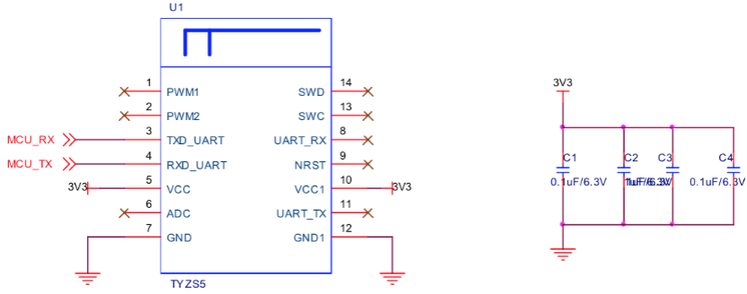
The P3 and P4 on the module are used for UART communication.
TYZS5 specifications
For more information about the TYZS5 module, see TYZS5 Module Datasheet.
The TYZS5 module provides the following pins for smart door locks: 3.3V pin, GND, TX and RX.
Antenna design
The TYZS5 module provided by Tuya applies to door locks. However, the metal structure of door locks might have an impact on the RF performance of antennas. Therefore, in the early layout design, the position and overall structure of an antenna must be optimized to minimize the impact on the RF performance.
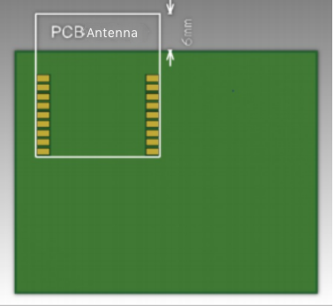
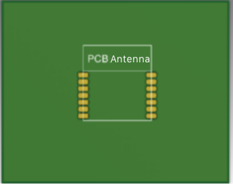
PCB antennas
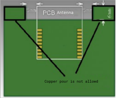
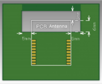
When a PCB onboard antenna is used in the Zigbee module, it is recommended that the distance between the module antenna and other metal parts should be at least 15 mm, in order to optimize the wireless performance. Trace and copper pour are not allowed in the antenna area of the PCB, in order not to affect the antenna performance. It is recommended to hollow out the adapter board in the antenna area.
The following figures show the recommended PCB layouts with the antenna.
It is recommended that the distance between the module antenna and other metal parts should be at least 15 mm, in order to optimize the RF performance. Through the surface mount technology (SMT) process, TYZS5 is attached to the main control board to work with other components. The position and placement of the PCB antenna directly affect the RF performance.
The following are positions that are recommended and not recommended. The antenna of the TYZS5 module is placed as shown in the figure. It is recommended to use the placement positions of Option 2 and Option 3. The antenna is outside the board frame, or the board near the antenna must be hollowed out. The performance is basically the same as the RF test performance of a single module. If the PCB antenna must be placed on the bottom plate due to design restrictions, you can refer to the placement of Option 4. The antenna is inside the board frame, but there is no copper pour and wiring near the antenna. However, it will cost some RF performance, almost with an attenuation of 1–2 dBm. It is not recommended to use the placement position of Option 5. The antenna is inside the board frame, and there is copper pour or wiring below the antenna. The RF signal will be significantly attenuated.
The antenna is inside the backplane
The antenna is located along the backplane frame. No copper pour area is allowed inside the frame.
The antenna is located along the midline of the backplane. The backplane frames around the antenna are hollowed out.
The antenna is inside the backplane. The lower areas are not kept clearance.
Based on the preceding PCB layout solutions, no substrate medium or metal part of the whole device exists directly below or directly above the PCB antenna. The PCB antenna is away from the copper sheet. This can maximize the radiation effect of the antenna.
Is this page helpful?
YesFeedbackIs this page helpful?
YesFeedback


