Smart LED Driver Design
This topic describes information about power supply development for the light-emitting diode (LED) driver that is required to build smart LED products.
Background information
To build smart LED products, you must integrate wireless components that support protocols such as Wi-Fi, Zigbee, and Bluetooth Low Energy (Bluetooth LE) into the traditional LED driver design. This allows you to improve multiple functions such as dimming, color changing, remote control, and smart linkage for smart LED products. Therefore, based on a power supply solution that supports normal LED working conditions, the LED driver design must meet the requirements on the power supply of wireless components.
Architecture
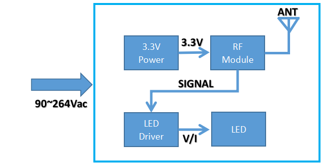
Step 1: Select a power supply solution for an RF module
A radio-frequency (RF) module features a high instantaneous peak current and a low average current. Therefore, when you select a power supply solution for the module, you must check the average current and instantaneous current in the module datasheet. The following sections describe multiple power supply solutions for RF modules:
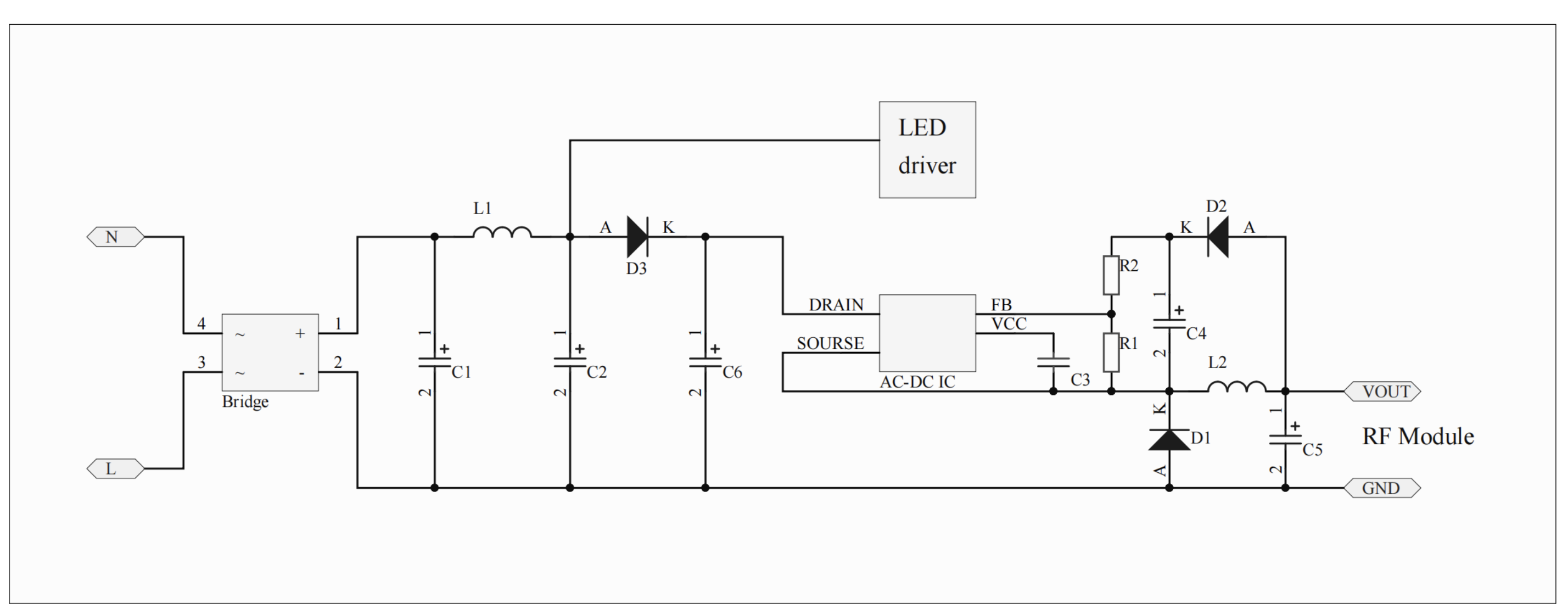
AC-DC constant voltage output
In this solution, an AC-DC constant voltage integrated circuit (IC) is used to convert high voltage from the VBUS pin to 3.3V constant voltage and power the module.
Things to note
-
A diode and a capacitor must be used to separate the AC-DC power supply circuit from the LED driver. This can minimize the impact on the primary power supply and ensure module performance. Particularly, for the linear constant-current power supply, this isolation mechanism can be used to avoid light flickering.
-
The output voltage ripple must be less than 100 mV. This can avoid an output voltage that is higher than or lower than the working voltage threshold of the module after the ripple is superimposed on the average voltage.
-
The AC-DC power supply solution must support the average output current that is at least twice the maximum average current of the RF module in all states. The output dynamic current must support the instantaneous peak current of the module. The following table lists the recommended AC-DC power supply parameters for each RF module.
RF module Average output current Maximum dynamic current Wi-Fi module 200 mA/3.3V 450 mA Bluetooth LE module 50 mA/3.3V 100 mA Zigbee module 50 mA/3.3V 100 mA -
The total capacitance of the electrolytic capacitor at the bus voltage terminal must be selected based on the accumulated value of the LED driver load and the RF module load.
-
In the scenarios of low standby power consumption, the AC-DC driver IC of low standby power consumption must be used to support the module of low standby current.
-
For more information about the design of AC-DC constant voltage circuits, see Power Design.
DC-DC constant voltage output
In this solution, the module is powered by the post-stage low-voltage constant-voltage terminal of the LED driver. In this case, the DC-DC constant-voltage IC is used to convert voltage and output 3.3V constant voltage. This solution applies to cool and warm white and multi-color (RGBCW) LED lights.
Things to note
- If the post-stage low-voltage constant-voltage terminal of the LED driver outputs a voltage of higher than 12V, we recommend that you do not use a low-dropout (LDO) regulator to step down the voltage to 3.3V. To power the module, you can use a DC-DC converter IC to step down the voltage to 3.3V. The DC-DC power supply solution must support the average output current that is at least twice the maximum average current of the RF module in all states. The output dynamic current must support the instantaneous peak current of the module. For more information about the recommended power supply parameters for each RF module, see the preceding table.
- We recommend that you do not use an LDO regulator in the power supply for a Wi-Fi module. Specific limits apply to the LDO regulator solution. For example, if an LDO is used, the power supply current of the IC must be 500 mA or higher. The heat dissipation performance must meet your business requirements.
- If an LDO is used, you must consider the value of LDO power consumption. This value is the dropout between the pre-stage voltage and post-stage voltage of the LDO multiplied by the LDO current. A higher voltage dropout results in higher power consumption of the LDO. The maximum current of the LDO must support the peak current of the module. If the peak current of the module reaches the maximum LDO current, LDO protection might be triggered. In this case, the output voltage collapse might occur and the module cannot work as expected.
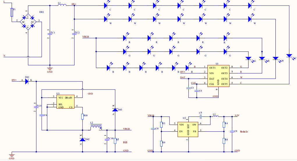
- In the buck circuit based on the DC-DC converter IC, the area of the following primary power loops must be minimized:
- Loop 1: Signals run through the following components in sequence: the anode of C8, U2, L3, the anode of C9, the cathode of C9, and the cathode of C8.
- Loop 2: Signals run through the following components in sequence: the switch (SW) pin of U2, L3, the anode of C9, the cathode of C9, and the ground pin of U2.
- In the buck circuit based on the DC-DC converter IC, the feedback resistor and filter capacitor must be close to the IC pins.
Linear dimming and lower-energy modules
In this solution, linear dimming is supported by the LED driver and low-energy modules such as Bluetooth or Zigbee modules are used. To enable the linear dimming function and ensure high LED driver efficiency, a small dropout is recommended between the output voltage and the input voltage. In the case of an input power outage, when the electrolytic capacitor input voltage is lower than the output voltage, the LED light goes out. However, the input capacitor still provides high residual voltage. Therefore, the dummy load and the AC-DC power supply are used to discharge the input capacitor. In most cases, the capacitor of the primary power supply provides high capacitance. Bluetooth and Zigbee modules feature low power consumption. Therefore, the module power supply requires a long-term normal voltage. This does not apply when rapid and continuous power-on and power-off operations are required to reset module pairing information.
To fix this issue, the power supply solution must be optimized. Specifically, the diode D1 is used to separate the circuit of the primary power supply from the power supply circuit of the module. The capacitor C3 is connected to the cathode of the diode. C1 and C2 provide low capacitance. This way, in the case of an input voltage outage, C1 and C2 capacitors increase the discharging efficiency. The dropout rate at the 3.3V power pin is also increased. This enables rapid and continuous power-on and power-off operations to reset module pairing information. After the outage, the voltage of C3 is higher than the voltage of C2. Therefore, in most cases, the blocking diode D1 is a rectifier diode with a breakdown voltage of higher than 600V.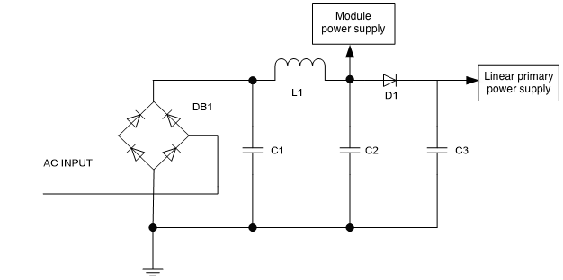
Step 2: Select a power supply solution for an LED driver
One-channel dimming for an AC-DC constant current driver
Switching power supply solution
In this solution, the module outputs pulse-width modulation (PWM) signals.
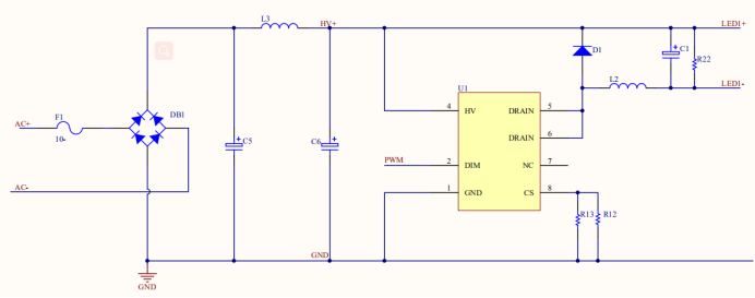
- Benefits: high efficiency, high power factors (PFs), excellent constant current performance and linearity, and a wide adjustable range of output voltage.
- Disadvantages: poor anti-electromagnetic interference (EMI) performance, high costs, noisy PWM dimming signals, and a complex printed circuit board (PCB) layout.
- Things to note
- The LED driver IC is integrated with a high-voltage metal-oxide-semiconductor (MOS) transistor. The IC generates a large amount of heat when the MOS transistor is working. To minimize the thermal resistance and improve the heat dissipation performance, the copper area on the heat dissipation pin of the IC must be maximized.
- The traces among the IC drain pins, inductor pins, and diode pins must be as short and wide as possible.
- The PWM signal traces from the module pins to the IC pins must be as short as possible. This can protect the PWM signals from noisy signals on the PCB.
- The distance between high-voltage traces and low-voltage traces must be optimized.
Linear solution
In this solution, the module outputs PWM signals.
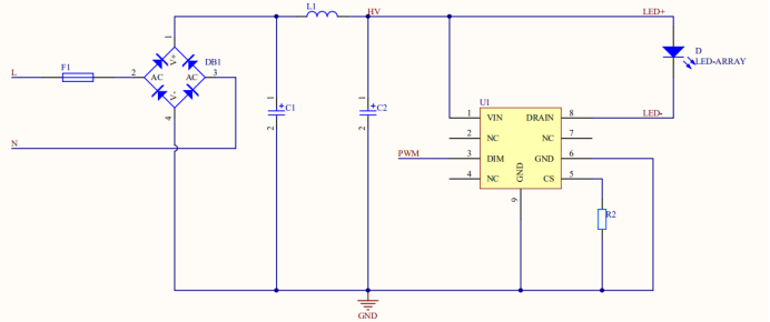
- Benefits: low costs, free of EMI issues, a simple PCB layout, and noise-free PWM dimming.
- Disadvantages: low efficiency, poor constant current performance in a narrow voltage range, unexpected linearity, fixed output voltage, and low PFs.
- Things to note
- The LED driver IC is integrated with a high-voltage MOS transistor. The IC generates a large amount of heat when the MOS transistor is working. To minimize the thermal resistance and improve the heat dissipation performance, the copper area on the heat dissipation pin of the IC must be maximized.
- The PWM signal traces from the module pins to the IC pins must be as short as possible. This can protect the PWM signals from noisy signals on the PCB.
- The distance between high-voltage traces and low-voltage traces must be optimized.
Two-channel dimming for an AC-DC constant current driver
The two-channel dimming solution supports the following control methods: cool and warm (CW) white light control and correlated color temperature (CCT) control.
CW white light control is implemented by two channels of PWM signals. Each channel is used for mixed control of brightness and color temperature. The cool-white (CW) channel controls white light (high color temperature). The warm-white (WW) channel controls warm light (low color temperature). The CW channel is used for single-channel dimming.
For the CCT control method, brightness control is separated from color temperature control based on two signal channels. One channel controls brightness and the other channel controls color temperature.
Switching power supply with CW control
In this solution, the module outputs two channels of PWM signals: CW control and WW control.
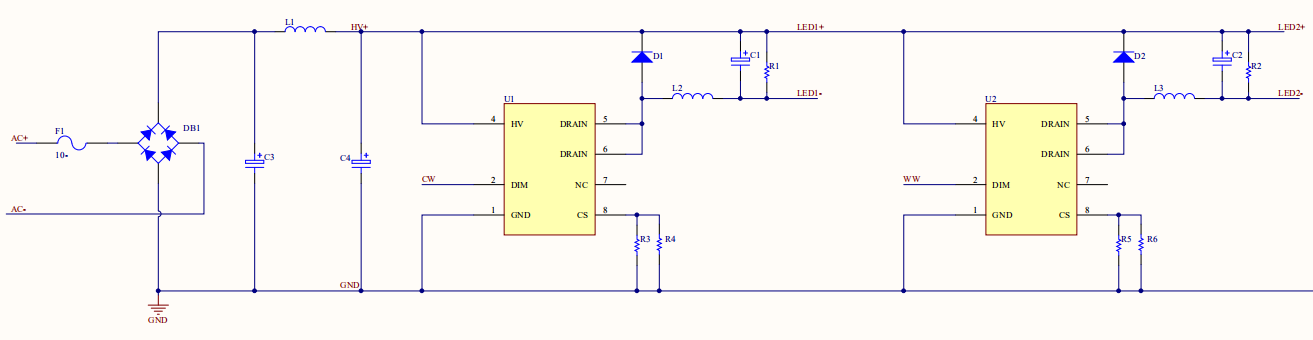
- Benefits: high efficiency, excellent constant current performance and linearity, and expected dimming effect.
- Disadvantages: poor anti-EMI performance, noisy circuits, large color temperature shift for a small duty cycle, a complex circuit layout, and high costs.
- Things to note
- The LED driver IC is integrated with a high-voltage MOS transistor. The IC generates a large amount of heat when the MOS transistor is working. To minimize the thermal resistance and improve the heat dissipation performance, the copper area on the heat dissipation pin of the IC must be maximized.
- The traces among the IC drain pins, inductor pins, and diode pins must be as short and wide as possible.
- The PWM signal traces from the module pins to the IC pins must be as short as possible. This can protect the PWM signals from noisy signals on the PCB.
- The distance between high-voltage traces and low-voltage traces must be optimized.
CW control
In this solution, the module outputs two channels of PWM signals: CW control and WW control.
- Benefits: low costs, free of EMI issues, a simple PCB layout, and noise-free PWM dimming.
- Disadvantages: low efficiency, poor constant current performance in a narrow voltage range, unexpected linearity, fixed output voltage, and large color temperature shift for a small duty cycle.
- Things to note
- The LED driver IC is integrated with a high-voltage MOS transistor. The IC generates a large amount of heat when the MOS transistor is working. To minimize the thermal resistance and improve the heat dissipation performance, the copper area on the heat dissipation pin of the IC must be maximized.
- The PWM signal traces from the module pins to the IC pins must be as short as possible. This can protect the PWM signals from noisy signals on the PCB.
- The distance between high-voltage traces and low-voltage traces must be optimized.
CCT control
In this solution, the module outputs two channels of PWM signals: brightness control and CCT control.
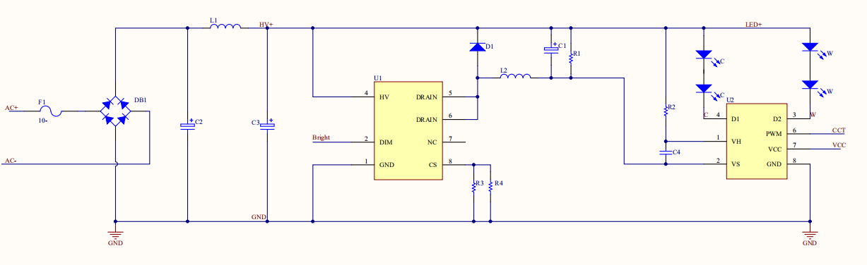
- Benefits: high efficiency, excellent constant current performance and linearity, expected dimming effect, noise-free analog brightness control, a simple circuit layout, and low costs.
- Disadvantages: poor anti-EMI performance, little color temperature shift, and higher costs than linear CW control.
- Things to note
- The LED driver IC is integrated with a MOS transistor. The IC generates a large amount of heat when the MOS transistor is working. To minimize the thermal resistance and improve the heat dissipation performance, the copper area on the heat dissipation pin of the IC must be maximized.
- The PWM signal traces from the module pins to the IC pins must be as short as possible. This can protect the PWM signals from noisy signals on the PCB.
- The distance between high-voltage traces and low-voltage traces must be optimized.
- The bypass capacitor C1 must be a low equivalent series resistance (ESR) bypass capacitor. The high ESR increases the efficiency loss.
- The saturation current of the power inductor L2 must be 30% to 50% higher than the output current. When the current capability meets your business requirements, the inductance can be slightly increased. This can improve the constant current performance.
- To maximize the efficiency and performance of the smart LED driver, the diode D1 must be a Schottky diode that features fast recovery, low forward voltage drop, low parasitic capacitance, and low leakage. The current capability and withstand voltage depend on specific applications, but the redundancy of 30% must be provided to ensure service stability and reliability.
Note: The diode must ensure the reverse current capability when the temperature is lower than 85°C.
- The drain pin of U1 is located on the fast switching node. Therefore, the PCB trace must be as short as possible and the ground terminal of the IC be well grounded.
- The parasitic inductance that is caused by the traces between the current sampling resistors R3 and R4 must be minimized to ensure the accuracy of sampling.
- The copper foil area of the D1 and D2 pins for U2 must be maximized to improve the heat dissipation performance.
- The bypass capacitor of the IC pins must be close to the IC pins.
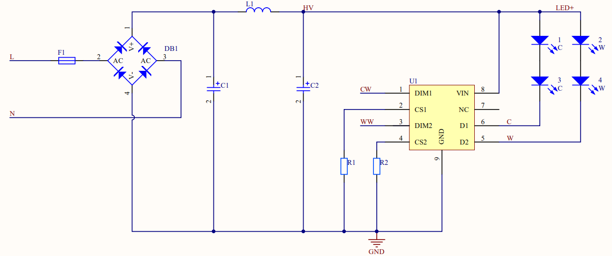
Three-channel dimming for a constant-current RGB driver
DC-DC linear constant-current driver with PWM control
In this solution, the module outputs three channels of PWM signals: PWMR, PWMG, and PWMB. The linear constant-current driver can enable constant output of red, green, blue (RGB) current.
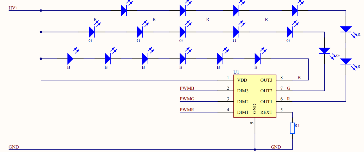
Things to note
- The LED driver IC is integrated with a high-voltage MOS transistor. The IC generates a large amount of heat when the MOS transistor is working. To minimize the thermal resistance and improve the heat dissipation performance, the copper area on the heat dissipation pin of the IC must be maximized.
- The PWM signal traces from the module pins to the IC pins must be as short as possible. This can protect the PWM signals from noisy signals on the PCB.
- The distance between high-voltage traces and low-voltage traces must be optimized.
DC-DC linear constant current drive with IIC control
In this solution, Inter-Integrated Circuit (IIC) control requires the data (DAT) and clock (CLK) pins to control three-channel or five-channel LEDs. Few control pins are used in this solution to minimize the load of module pins. The module outputs DAT and CLK IIC signals to the driver IC to control the RGB constant current. In this solution, PCB layout traces must be optimized.
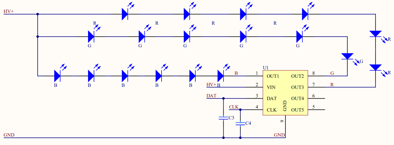
Things to note
- The LED driver IC is integrated with a high-voltage MOS transistor. The IC generates a large amount of heat when the MOS transistor is working. To minimize the thermal resistance and improve the heat dissipation performance, the copper area on the heat dissipation pin of the IC must be maximized.
- The distance between high-voltage traces and low-voltage traces must be optimized.
- IIC signals are susceptible to interference from switching signals that are sent by the AC-DC driver circuit. To minimize the interference, we recommend that you connect filter capacitors (10 pF to 50 pF) with the DAT and CLK pins to filter signals in the PCB layout.
- Pull-up resistors must be added to the peripheral DAT and CLK signals of the module when IIC signals are processed. The resistance is recommended to be 4.7 kΩ and can be modified based on the application requirements.
DC-DC BJT or MOS switching driver with PWM control
In this solution, a bipolar junction transistor (BJT) or a MOS transistor is used to transmit PWM switching signals and control RGB LEDs. RGB LEDs do not support constant current, but feature current dispersion. In the same input conditions, a low voltage is applied to red LEDs. Therefore, a resistor is added to the red LED trace to limit current. However, this increases unnecessary power consumption. A low voltage dropout is applied between the lamp bead voltage and the input voltage.
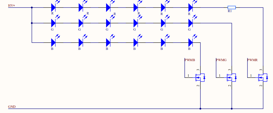
Things to note
- The LED driver IC is integrated with a high-voltage MOS transistor. The IC generates a large amount of heat when the MOS transistor is working. To minimize the thermal resistance and improve the heat dissipation performance, the copper area on the heat dissipation pin of the IC must be maximized.
- The distance between high-voltage traces and low-voltage traces must be optimized.
- The PWM signal traces from the module pins to the IC pins must be as short as possible. This can protect the PWM signals from noisy signals on the PCB.
Five-channel dimming for an AC-DC IIC linear constant current driver
In this solution, RGB lights are powered separately from the CW white lights. We recommend that you use both the AC-DC and DC-DC solutions to power the module.
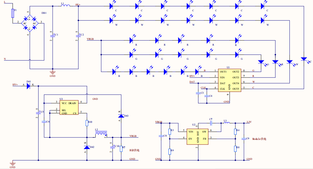
- Benefits: a simple layout, simple peripheral parameters, low costs, and easy control of only DAT and CLK signals.
- Disadvantages: DAT and CLK signals are vulnerable to interference from the linear constant-current driver.
- Things to note
- The LED driver IC of U1 is integrated with a high-voltage MOS transistor. The IC generates a large amount of heat when the MOS transistor is working. To minimize the thermal resistance and improve the heat dissipation performance, the copper area on the heat dissipation pin of the IC must be maximized.
- The distance between high-voltage traces and low-voltage traces must be optimized.
- IIC signals are susceptible to interference from switching signals that are sent by the AC-DC driver circuit. To minimize the interference, we recommend that you connect filter capacitors (10 pF to 50 pF) with the DAT and CLK pins to filter signals in the PCB layout.
- Pull-up resistors must be added to the peripheral DAT and CLK signals of the module when IIC signals are processed. The resistance is recommended to be 4.7 kΩ and can be modified based on the application requirements.
- For more information about the design of AC-DC constant voltage circuits, see Power Design.
- In the buck circuit based on the DC-DC converter IC, the area of the following primary power loops must be minimized:
- Loop 1: Signals run through the following components in sequence: the anode of C8, U2, L3, the anode of C9, the cathode of C9, and the cathode of C8.
- Loop 2: Signals run through the following components in sequence: the switch (SW) pin of U2, L3, the anode of C9, the cathode of C9, and the ground pin of U2.
- In the buck circuit based on the DC-DC converter IC, the feedback resistor and filter capacitor must be close to the IC pins.
Is this page helpful?
YesFeedbackIs this page helpful?
YesFeedback


