Power Design
This topic describes information about the hardware development of the AC-DC non-isolated power supply solution.
Application scope
The AC-DC non-isolated power supply solution is a streamlined low-power non-isolated switching power supply solution. This solution is developed based on a highly integrated constant-voltage controller chip as the core and a small number of peripheral circuits. This solution supports one or more of the topologies, such as the buck converter, boost converter, and buck-boost converter. The constant-voltage controller chip is embedded with a high-voltage metal–oxide–semiconductor (MOS) transistor. This structure supports multiple functions, such as overcurrent protection, undervoltage protection, and short-circuit protection.
Common topologies
Buck converter topology
Features
Non-isolated circuit, direct feedback, low power consumption, and positive output voltage. 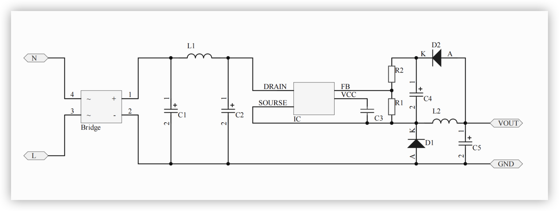
Buck-boost converter topology
Features
Non-isolated circuit, direct feedback, low power consumption, and negative output voltage. 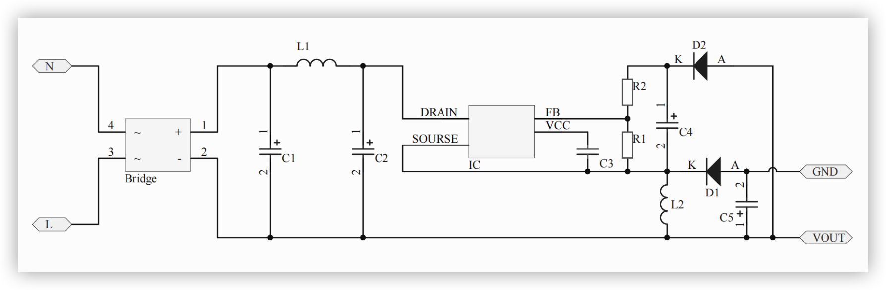
Boost converter topology
Features
Non-isolated circuit, direct feedback, low power consumption, and positive output voltage. 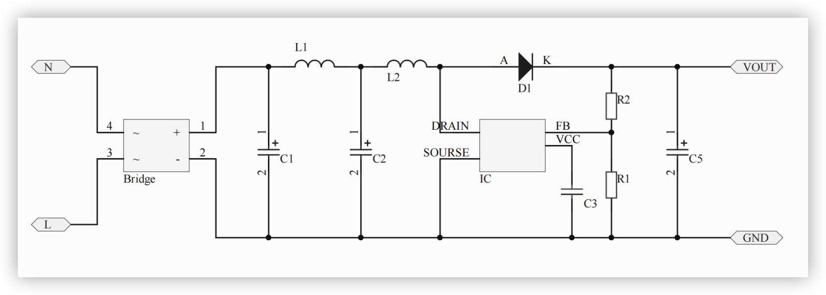
Circuit design
Chip
| Parameter | Description |
|---|---|
| Withstand voltage and internal resistance of the MOS transistor | The withstand voltage determines the maximum voltage that can be applied between the source and drain terminals during the operating time of the MOS transistor. The operating voltage higher than the withstand voltage might cause damage to the MOS transistor. The internal resistance of the MOS transistor affects the heat generation of the chip. When the same output power is used, the higher internal resistance increases the heat generation of the chip. |
| Working frequency | The audible range is from 2 kHz to 20 kHz. Therefore, we recommend that the power supply is designed with the working frequency beyond this range. You can also take measures to reduce the audio noise. The improper design of the power supply circuit might cause a working frequency of less than 20 kHz. In this case, when the inductor is charged and discharged within this frequency, howling might occur. |
| Static power consumption | The power consumption of the power supply under no-load condition. |
| Output current capability | The output current capability supports the continuous conduction mode and the discontinuous conduction mode. |
| Peak current limit or prospective short-circuit current | The value of this parameter for the selected power supply solution must be greater than the peak current of the load. |
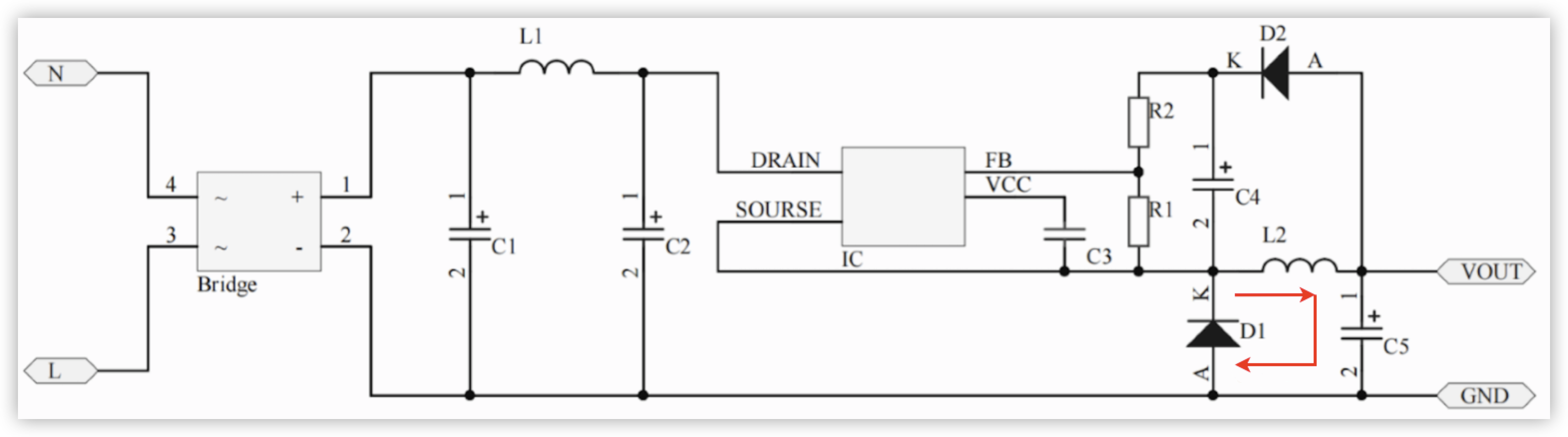
Input capacitor
In the preceding topology examples, C1 and C2 are used as input capacitors. To reduce noise, we recommend that you select electrolytic capacitors in the power supply solution. You also need to consider the withstand voltage and capacity.
| Parameter | Description |
|---|---|
| Withstand voltage | The value of this parameter must be greater than the maximum DC bus voltage if the maximum input voltage is applied. |
| Capacity | If the front-end half-wave rectification is used, the capacity of 3uF/W is recommended. If the front-end full-wave rectification is used, the capacity of 1.5uF/W to 2uF/W is recommended. The capacitance parameters that are provided by the manufacturer prevail due to the differences in chip design. |
| Bus voltage | The minimum DC bus voltage must support the minimum working voltage that is required by the power supply integrated circuit (IC). To improve the electromagnetic compatibility (EMC) in the circuit design, we recommend that you select a Pi filter that is composed of capacitors and inductors for bus voltage. |
Power inductor
In the preceding topology examples, L2 is used as a power inductor. For more information about the parameters, see the specifications of the power supply IC.
If an I-shaped inductor is used as a power inductor, the inductor must be as far away as possible from the input terminal. This prevents radiated coupling between the switching frequency and the input terminal. Otherwise, the EMC requirements might not be fulfilled.
Freewheeling diode
In the preceding topology examples, D1 is used as a freewheeling diode.
The synchronous rectification architecture can be used in chip design to avoid the use of freewheeling diodes. This simplifies the peripheral circuit.
| Parameter | Description |
|---|---|
| Reverse breakdown voltage | The value of this parameter must be greater than the maximum DC bus voltage. This applies to buck circuits and buck-boost circuits. |
| Current carrying capacity | The current carrying capacity must be twice or more the maximum output current of the load. |
| Reverse breakdown voltage | The reverse recovery time affects the conversion efficiency of the power supply. You must select a fast recovery diode. The reverse recovery time of 35 ns is recommended. |
Feedback diode
In the preceding topology examples, D2 is used as a feedback diode. A freewheeling diode must be a fast recovery diode. However, a feedback diode must be a slow diode, such as the 1N400x series diode. In this case, the forward voltage drop of the freewheeling diode and the feedback diode must be maintained.
Output capacitor
In the preceding topology examples, C5 is used as an output capacitor. To smooth the output voltage, we recommend that you select ceramic capacitors or low equivalent series resistance (ESR) electrolytic capacitors. This allows you to reduce the output voltage ripple.
Feedback resistor
In the preceding topology examples, R1 and R2 are used as feedback resistors. You can modify the resistance ratio to regulate the output voltage. The resistance or resistance range is recommended in general specifications. We recommend that you use the resistance within the recommended resistance range.
Anti-surge performance
- A fusible resistor or wirewound resistor can be used instead of a fuse. This method improves the anti-surge performance. A larger resistance value brings better anti-surge performance, but requires higher power.
- You can also increase the capacity of the input capacitor to bring better anti-surge performance. However, in this case, the dimensions and price of the capacitor are also increased.
- Add protection devices such as varistors.
PCB design
The design of a printed circuit board (PCB) determines the reliability, electromagnetic interference (EMI) performance, and thermal characteristics of the power supply. Therefore, when you design the PCB, the following notes must be considered:
-
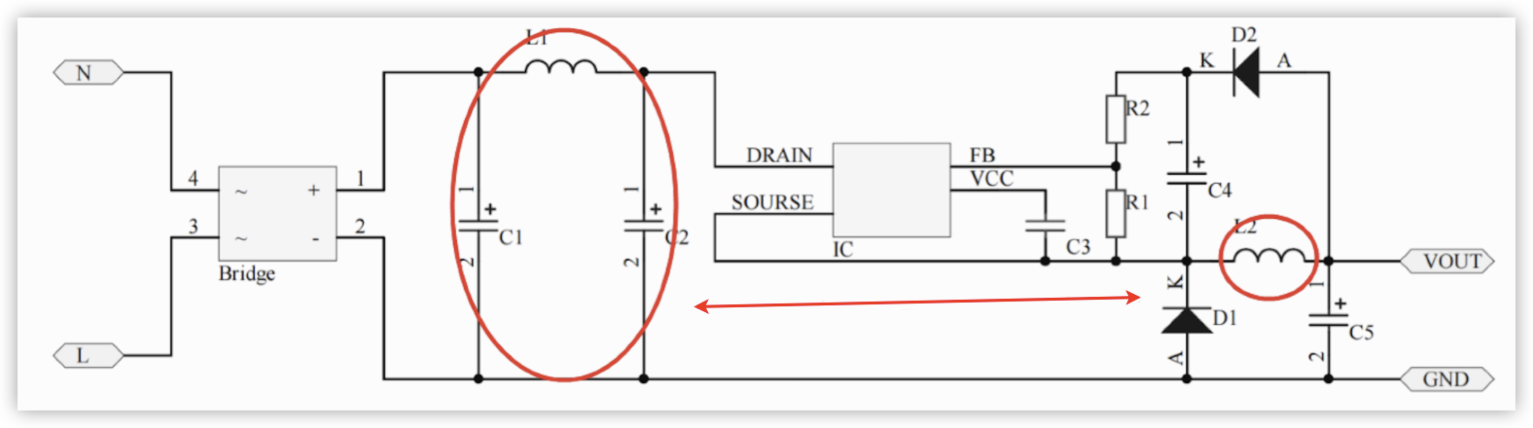
The area of loop 1 and loop 2 in a PCB layout must be as small as possible.
- Loop 1: Signals run through the following components in sequence: input capacitor C2, power supply IC, power inductor L2, output capacitor C5, and ground return.
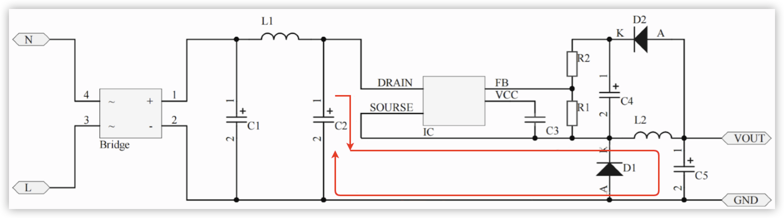
- Loop 2: Signals run through the following components in sequence: freewheeling diode D1, power inductor L2, output capacitor C5, and ground return.
- Loop 1: Signals run through the following components in sequence: input capacitor C2, power supply IC, power inductor L2, output capacitor C5, and ground return.
-
When the minimum loop area is used, power inductor L2 must be as far away as possible from the Pi filter circuit and the input terminal on the bus.
-
Feedback resistors R and R2 are placed close to the IC pins.
-
The bypass capacitor of the IC is placed close to the IC pins.
-
In the buck and buck-booster converter circuits, the drain terminal is the DC setpoint of the main power supply. You can increase the copper area on the primary current loop to improve the heat dissipation and performance of the power supply. The source terminal is the switching point of the power supply. This method minimizes the wire diameter between the source terminal and the power inductor and improves the EMI characteristics.
Power supply tests and indicators
Electrical performance test
| No. | Item | Condition | Indicator |
|---|---|---|---|
| 1 | Voltage stress withstand capability of the MOS transistor | The maximum voltage of drain-source voltage (VDS) is tested in the following conditions:
|
The measured value is less than 0.9 times the nominal value. |
| 2 | Current stress of the power inductor | The charging and discharging current waveforms of the power inductor are tested in the following conditions:
|
The inductor does not enter the magnetic saturation state. |
| 3 | Electrical performance parameters | The output voltage and its ripple and power conversion efficiency are measured in the following conditions:
|
The design requirements are fulfilled. |
| 4 | Dynamic response | The output voltage waveforms are observed in the following conditions:
|
The voltage waveforms show fluctuation within the allowable range. |
| 5 | Output voltage rise time | The output voltage waveforms are observed in the following conditions:
|
The rise time of the voltage waveforms is sufficient for the normal start of the load. |
| 6 | Temperature rise of components | The temperature of different components, such as heating components, power inductors, and electrolytic capacitors are tested in the following conditions:
|
The temperature of the components is within the nominal temperature range. The service life of the electrolytic capacitor must be calculated based on the temperature value. The calculated value must meet the requirements on the service life. |
Reliability test
| No. | Item | Condition | Indicator |
|---|---|---|---|
| 1 | Temperature rise of components | The temperature of different components, such as heating components, power inductors, and electrolytic capacitors are tested in the following conditions:
|
The temperature of the components is within the nominal temperature range. The service life of the electrolytic capacitor must be calculated based on the temperature value. The calculated value must meet the requirements on the service life. |
| 2 | Short-circuit test | The output is short-circuited and energized for 24 hours with normal working voltage. | The power supply survives the short circuit and continues to run as expected. |
| 3 | Switching test | The input voltage is repeatedly switched on and off 20,000 times. | The power supply survives the switching test and continues to run as expected. |
| 4 | Aging test | A small number of products are energized and aged in a high-temperature environment. | All of these products pass the test. |
EMC and safety test
| No. | Item | Condition | Indicator |
|---|---|---|---|
| 1 | EMI conduction test | The product is tested based on the test standards. | The test result meets the standards. |
| 2 | Radiation test | The product is tested based on the test standards. | The test result meets the standards. |
| 3 | lightning surge immunity test | The product is tested based on the test standards. | The product passes the test. |
| 4 | Electrostatic discharge test | The product is tested based on the test standards. | The product passes the test. |
Things to note
Specific types of devices such as Wi-Fi and Bluetooth devices feature low average current and high instantaneous current. When you develop these devices, the following things must be noted:
-
When you design the power supply, we recommend that you check whether the instantaneous current of these devices reaches the current limit threshold or the current limit protection value of the power supply IC. If so, power protection might be caused. In this mode, the power supply might be continuously restarted or output voltage collapse might occur.
If the instantaneous current of the loads is close to the peak current limit threshold of the power IC, you can test the stability of the power output by using the following tests:- Test 1: Simulate the current characteristics of these devices by using the dynamic load settings of the electronic loads. Test the dynamic response in the electrical performance test and observe whether the output voltage works fine.
- Test 2: Set these loads to the most severe state, power on them, and then observe whether the output voltage works fine.
- Solutions:
- Use the power supply solution with a high peak current limit threshold.
- Increase the capacitance of the output capacitor to supplement the instantaneous peak current output. However, you must consider the impact of the specified capacitance on the rise time of output voltage for the power supply.
-
If this type of load is repeatedly switched between heavy load and light load, audible current howling might occur in specific power supply applications.
Solutions:- Optimize the power supply parameters.
- Select an optimal power supply solution.
Is this page helpful?
YesFeedbackIs this page helpful?
YesFeedback


