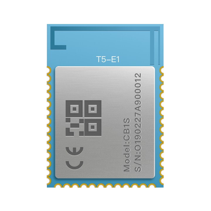
T5-E1 Modules
This topic is intended to provide hardware information and serve as the reference when you develop with T5-E1 modules. It helps you get an overall understanding of the product specifications and assists in developing products and applications.
Overview
T5-E1-IPEX is a highly integrated single-antenna single-band 2.4 GHz Wi-Fi 6 (IEEE 802.11b/g/n/ax) and Bluetooth 5.4 Low Energy (LE) combo IoT module. Featuring a multi-peripheral packaging and ultra-low-power chip, the T5-E1-IPEX module provides a highly integrated, efficient, secure, and lowest-power environment for IP cameras, HMI applications, smart locks, and other advanced IoT applications.
The T5-E1 module is embedded with an ARMv8-M Star (M33F) processor with a clock rate of up to 480 MHz, and integrates 8 MB flash memory, 16 MB PSRAM, 640 KB SRAM shared memory, and 64 KB ROM. Support interfaces such as USB, UART, SDIO, SPI, I2C, I2S, and ADC, as well as external devices such as displays, cameras, microphones, speakers, and microSD cards.
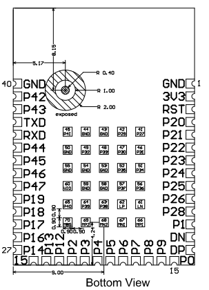
Appearance
Pins on module
T5-E1 is equipped with a total of 70 pins, including 40 LCC pins and 30 LGA pins.
The pinout is as follows:
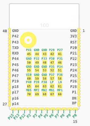
| No. | Name | I/O type | Description |
|---|---|---|---|
| 1 | GND | P | Ground pin |
| 2 | 3V3 | P | Power pin |
| 3 | RST | I | The low-level reset pin, active high, and pulled up internally |
| 4 | P20 | I/O |
|
| 5 | P21 | I/O |
|
| 6 | P22 | I/O |
|
| 7 | P23 | I/O |
|
| 8 | P24 | I/O |
|
| 9 | P25 | I/O |
|
| 10 | P26 | I/O |
|
| 11 | P28 | I/O |
|
| 12 | P1 | I/O |
|
| 13 | DN | I/O | USB D- |
| 14 | DP | I/O | USB D+ |
| 15 | P0 | I/O |
|
| 16 | P9 | I/O |
|
| 17 | P8 | I/O |
|
| 18 | P7 | I/O |
|
| 19 | P6 | I/O |
|
| 20 | P5 | I/O |
|
| 21 | P4 | I/O |
|
| 22 | P3 | I/O |
|
| 23 | P2 | I/O |
|
| 24 | P12 | I/O |
|
| 25 | P13 | I/O |
|
| 26 | P15 | I/O |
|
| 27 | P14 | I/O |
|
| 28 | P16 | I/O |
|
| 29 | P17 | I/O |
|
| 30 | P18 | I/O |
|
| 31 | P19 | I/O |
|
| 32 | P47 | I/O |
|
| 33 | P46 | I/O |
|
| 34 | P45 | I/O |
|
| 35 | P44 | I/O |
|
| 36 | RXD | I/O |
|
| 37 | TXD | I/O |
|
| 38 | P43 | I/O |
|
| 39 | P42 | I/O |
|
| 40 | GND | P | Ground pin |
| 41 | P27 | I/O |
|
| 42 | P29 | I/O |
|
| 43 | GND | P | Ground pin |
| 44 | GND | P | Ground pin |
| 45 | P41 | I/O |
|
| 46 | P31 | I/O |
|
| 47 | P30 | I/O |
|
| 48 | P33 | I/O |
|
| 49 | P32 | I/O |
|
| 50 | GND | P | Ground pin |
| 51 | P34 | I/O |
|
| 52 | P35 | I/O |
|
| 53 | GND | P | Ground pin |
| 54 | GND | P | Ground pin |
| 55 | GND | P | Ground pin |
| 56 | P36 | I/O |
|
| 57 | P37 | I/O |
|
| 58 | GND | P | Ground pin |
| 59 | GND | P | Ground pin |
| 60 | VIO | AO | GPIO LDO output |
| 61 | LN | AO | Audio left channel negative output |
| 62 | LP | AO | Audio left channel positive output |
| 63 | P38 | I/O |
|
| 64 | P39 | I/O |
|
| 65 | P40 | I/O |
|
| 66 | MP1 | AO | Microphone 1 positive input |
| 67 | MN1 | AO | Microphone 1 negative input |
| 68 | MN2 | AO | Microphone 2 negative input |
| 69 | MP2 | AO | Microphone 2 positive input |
| 70 | MBS | AO | Microphone bias output |
- The maximum input level for the ADC pin is 1.1V. It is recommended to use MΩ level external voltage divider resistors, and place a 100nF capacitor close to the ADC pin for grounding and filtering.
Pindicates the power pin.I/Oindicates the input and output pin.AIindicates the analog signal input pin.AOindicates the analog signal output pin.
Pin configuration and features
UART
Pin description
The module provides three UART interfaces:
-
UART 0: used to connect to your MCU. The serial data transmission follows Tuya’s protocol. The baud rate is 115200 bps by default.
-
UART 1: used to connect to peripheral devices.
-
UART 2: used to connect to peripheral devices.
Pin No. Signal Feature 36 DL_UART_RX UART 0. It can be used as a download port to receive data. 37 DL_UART_TX UART 0. It can be used as a download port to transmit data. 12 UART1_RX UART 1 to receive data. 15 UART1_TX UART 1 to transmit data. 45 UART2_TX UART 2 to transmit data. 65 UART2_RX UART 2 to receive data.
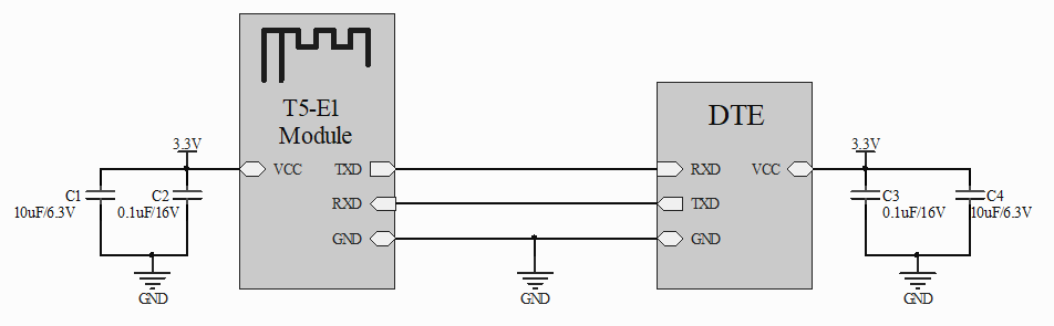
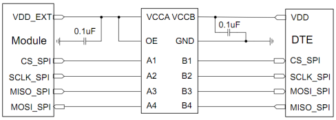
Serial communication between module and MCU
-
Connection between a module and a 3.3V MCU
-
Connection between a module and a 5V MCU
In the following circuit diagram, voltage level translation can be implemented with a bidirectional voltage-level translator, a MOS transistor, or a triode.
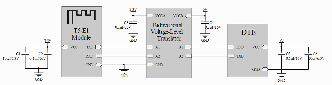
Level translator reference
-
N-channel MOSFET level translator: An N-channel MOSFET and a built-in body diode are used to implement two-way communication.
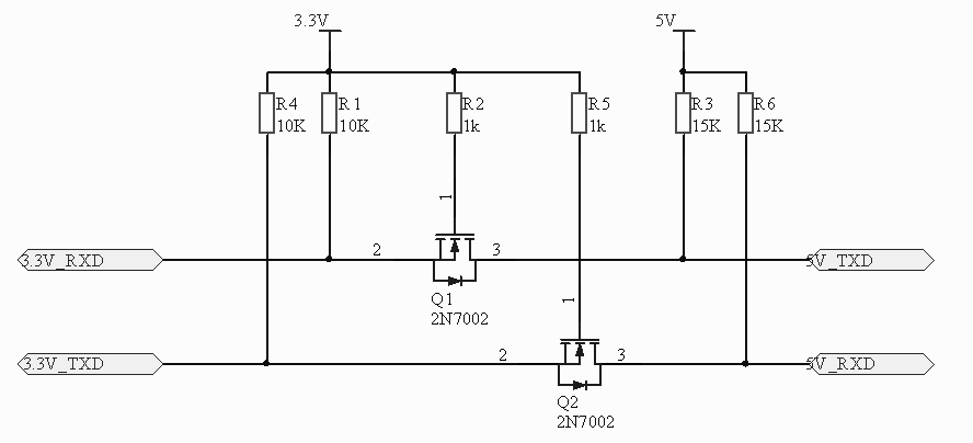
-
NPN triode level translator: An NPN triode is used to implement one-way communication.
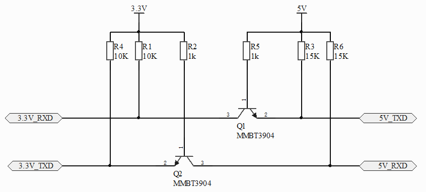
See the circuit diagram above for how UART 1, UART 2, and UART 0 are connected.
Circuit design
The UART trace should be as short as possible. Add ground vias around the UART and keep away from RF and periodic signal lines.
USB
Pin description
The USB interface conforms to USB 2.0 specifications.
| Pin No. | Signal | Feature |
|---|---|---|
| 13 | USB_DN |
USB high-speed differential transceiver (negative). It supports high-speed and full-speed modes. |
| 14 | USB_DP |
USB high-speed differential transceiver (positive). It supports high-speed and full-speed modes. |
Applications
-
MCU solutions
-
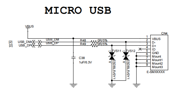
Micro-USB cable
Circuit design
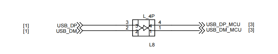
- Make sure to route the USB signal traces as differential pairs with total grounding, keeping them parallel and of equal length. The impedance of USB differential trace is 90Ω.
- Do not route signal traces under the power supply, RF signal traces, and other sensitive signal traces. It is important to route the USB differential traces in the inner layer with ground shielding on not only the upper and lower layers but also the right and left sides.
- Connect a common mode choke between the MCU and module in series to improve EMI suppression.
- Considering connection to micro-USB devices, place the TVS diode as close to the USB port as possible with a parasitic capacitance of less than 2 pF.
SPI
The T5-E1 module has two sets of SPI interfaces, and the following table details the pins:
| Pin No. | Signal | Feature |
|---|---|---|
| 26 | SPI0_CSN | GPIO15, SPI0 chip select signal |
| 28 | SPI0_MOSI | GPIO16, SPI0 controller out and agent in |
| 29 | SPI0_MISO | GPIO17, SPI0 controller in and agent out |
| 27 | SPI0_SCK | GPIO14, SPI0 clock signal |
| 22 | SPI1_CSN | GPIO3, SPI1 chip select signal |
| 21 | SPI1_MOSI | GPIO4, SPI1 controller out and agent in |
| 20 | SPI1_MISO | GPIO5, SPI1 controller in and agent out |
| 23 | SPI1_SCK | GPIO2, SPI1 clock signal |
Electrical specifications and applications
The voltage level of the SPI interface on this module is 3.3V. A level translator should be used if the application is equipped with a 5V UART interface. A level translator for SPI is recommended.
The reference circuit is shown in the figure below:
QSPI
The T5-E1 module has two sets of QSPI interfaces, and the following table details the pins:
| Pin No. | Signal | Feature |
|---|---|---|
| 6 | QSPI0_SCK | GPIO22, QSPI0 clock signal |
| 7 | QSPI0_CS | GPIO23, QSPI0 enable signal |
| 8 | QSPI0_IO0 | GPIO24, QSPI0 data bit 0 |
| 9 | QSPI0_IO1 | GPIO25, QSPI0 data bit 1 |
| 10 | QSPI0_IO2 | GPIO26, QSPI0 data bit 2 |
| 41 | QSPI0_IO3 | GPIO27, QSPI0 data bit 3 |
| 18 | QSPI1_IO3 | GPIO7, QSPI1 data bit 3 |
| 19 | QSPI1_IO2 | GPIO6, QSPI1 data bit 2 |
| 20 | QSPI1_IO1 | GPIO5, QSPI1 data bit 1 |
| 21 | QSPI1_IO0 | GPIO4, QSPI1 data bit 0 |
| 22 | QSPI1_CS | GPIO3, QSPI1 enable signal |
| 23 | QSPI1_SCK | GPIO2, QSPI1 clock signal |
If you need to flash the firmware to the external flash that is already soldered on the board, the hardware design must ensure that T5 and the external flash are not sharing the same power supply or are isolated. Reserve test points for the corresponding flashing pins (3V3, GND, QSPI_IO0, QSPI_IO1, QSPI_IO2, QSPI_IO3, QSPI_CS, QSPI_SCK). When using a writer to flash the firmware to the external flash, make sure the flash is powered on independently and T5 is not powered on.
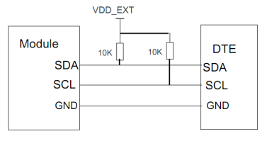
I2C
The T5-E1 module has two sets of I2C interfaces, and the following table details the pins:
| Pin No. | Signal | Feature |
|---|---|---|
| 4 | I2C0_SCL | GPIO20, I2C0 clock signal |
| 5 | I2C0_SDA | GPIO21, I2C0 data signal |
| 15 | I2C1_SCL | GPIO0, I2C1 clock signal |
| 12 | I2C1_SDA | GPIO1, I2C1 data signal |
I2C is a simple serial communication bus protocol that uses just two bus wires, a serial data wire (SDA) and a serial clock wire (SCL). I2C is integrated into many ICs and allows devices to communicate directly with each other. Each device is recognized by a unique address to differentiate from other devices on the same I2C bus and can operate either as a transmitter or a receiver depending on its function.
Applications
The I2C bus must be pulled up on the device.
I2S
The T5-E1 module has three sets of I2S interfaces, and the following table details the pins:
| Pin No. | Signal | Feature |
|---|---|---|
| 11 | I2S_MCLK | GPIO28, main clock signal |
| 16 | I2S0_DOUT | GPIO9, I2S0 output signal |
| 17 | I2S0_DIN | GPIO8, I2S0 input signal |
| 18 | I2S0_SYNC | GPIO7, I2S0 sync signal |
| 19 | I2S0_SCK | GPIO6, I2S0 clock signal |
| 32 | I2S2_DOUT | GPIO47, I2S2 output signal |
| 33 | I2S2_DIN | GPIO46, I2S2 input signal |
| 34 | I2S2_SYNC | GPIO45, I2S2 sync signal |
| 35 | I2S2_SCK | GPIO44, I2S2 clock signal |
| 38 | I2S1_DOUT | GPIO43, I2S1 output signal |
| 39 | I2S1_DIN | GPIO42, I2S1 input signal |
| 45 | I2S1_SYNC | GPIO41, I2S1 sync signal |
| 65 | I2S1_SCK | GPIO40, I2S1 clock signal |
SDIO
The T5-E1 module has one set of SDIO interfaces, and the following table details the pins:
| Pin No. | Signal | Feature |
|---|---|---|
| 20/29 | SDIO_DATA1 | GPIO5/GPIO17, SDIO data bit 1 |
| 21/28 | SDIO_DATA0 | GPIO4/GPIO16, SDIO data bit 0 |
| 22/26 | SDIO_CMD | GPIO3/GPIO15, SDIO command |
| 23/27 | SDIO_CLK | GPIO2/GPIO14, SDIO clock |
| 36/30 | SDIO_DATA2 | UART0_RX/GPIO18, SDIO data bit 2 |
| 37/31 | SDIO_DATA3 | UART0_TX/GPIO19, SDIO data bit 3 |
Applications
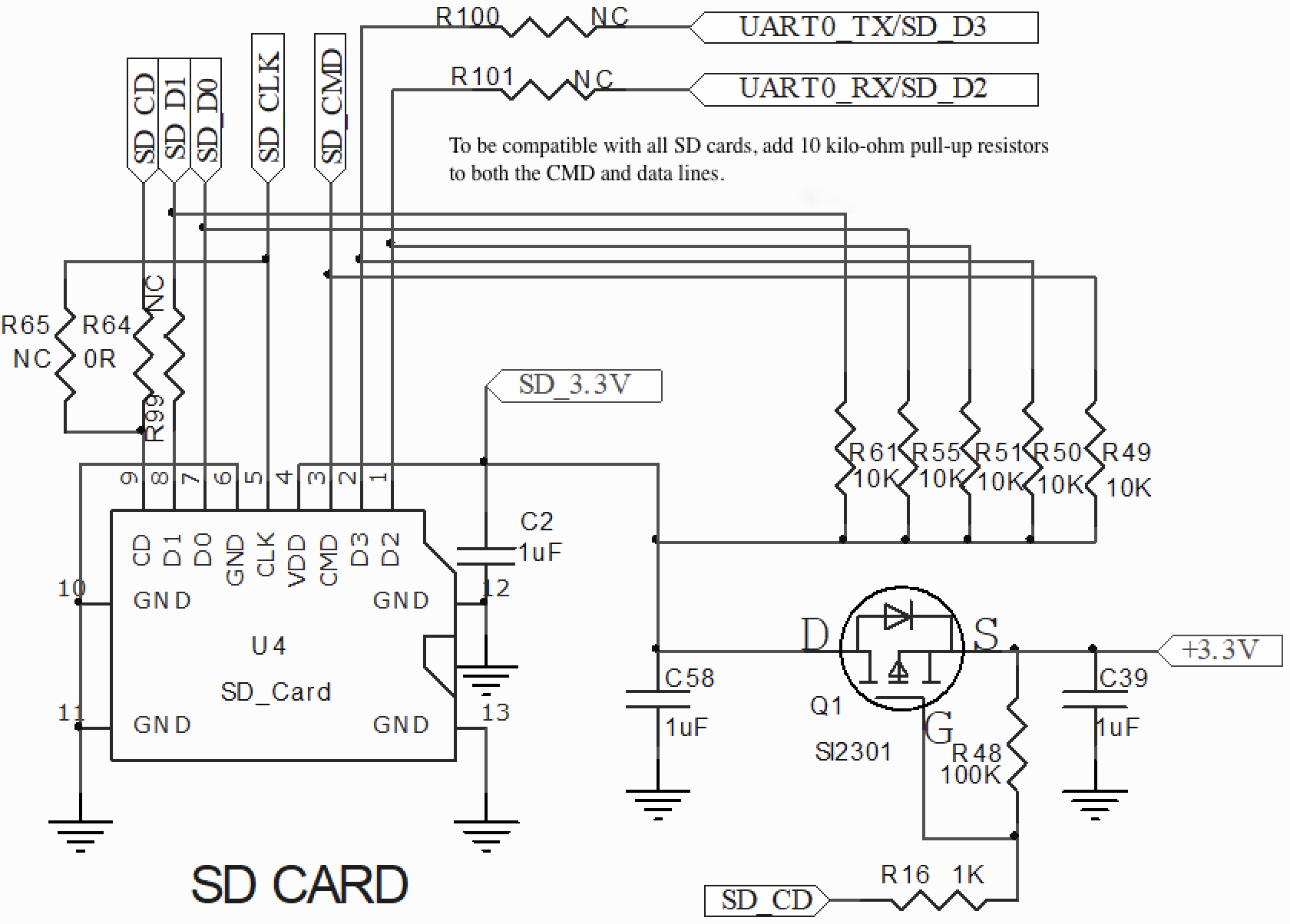
Circuit design
- Reserve a 22Ω resistor between the
SD_CLKand SD signal trace in series to reduce RF interference. - Reserve a pad for 0201 33 pF capacitor on the SD signal trace.
SD_DATA[0:3]andSD_CMDhave reserved pull-up resistors to increase bus stability.- The
SD_CLKsignal trace needs ground shielding individually. Its length should be as short as possible, within 2,500 mil, preferably within 2,000 mil. Surround SD signal traces with total grounding to prevent any possible crosstalk and noise coupling from other signal sources. - It is recommended to keep the same trace length for
SD_CLK,SD_DATA[0:3], andSD_CMD, with a length difference of less than 1 mm. The total length should not exceed 50 mm. - In order to offer good ESD protection, it is recommended to add an ESD diode array with a parasitic capacitance of less than 15 pF. The ESD protection device should be placed as close as possible to the SIM card connector 3V3,
SD_CLK,SD_DATA[0:3], andSD_CMD. Make sure the SIM card signal lines go through the ESD protection device first and then to the module.
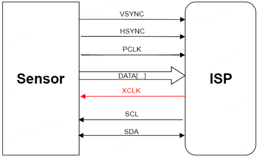
Camera
Pin description
| Pin No. | Signal | Feature |
|---|---|---|
| 41 | CIS_MCLK | GPIO27, driver clock that is output to the sensor |
| 42 | CIS_PCLK | GPIO29, pixel clock |
| 46 | CIS_VSYNC | GPIO31, frame sync signal |
| 47 | CIS_HSYNC | GPIO30, horizontal sync signal |
| 48 | CIS_PXD1 | GPIO33, pixel data, data bit 1 |
| 49 | CIS_PXD0 | GPIO32, pixel data, data bit 0 |
| 51 | CIS_PXD2 | GPIO34, pixel data, data bit 2 |
| 52 | CIS_PXD3 | GPIO35, pixel data, data bit 3 |
| 56 | CIS_PXD4 | GPIO36, pixel data, data bit 4 |
| 57 | CIS_PXD5 | GPIO37, pixel data, data bit 5 |
| 63 | CIS_PXD6 | GPIO38, pixel data, data bit 6 |
| 64 | CIS_PXD7 | GPIO39, pixel data, data bit 7 |
DVP requires a set of I2C interfaces to configure the sensor.
Applications
RGB565
Pin description
| Pin No. | Signal | Feature |
|---|---|---|
| 31 | RGB_R7 | GPIO19, RGB red component, data bit 7 |
| 4 | RGB_R6 | GPIO20, RGB red component, data bit 6 |
| 5 | RGB_R5 | GPIO21, RGB red component, data bit 5 |
| 6 | RGB_R4 | GPIO22, RGB red component, data bit 4 |
| 7 | RGB_R3 | GPIO23, RGB red component, data bit 3 |
| 8 | RGB_G7 | GPIO24, RGB green component, data bit 7 |
| 9 | RGB_G6 | GPIO25, RGB green component, data bit 6 |
| 10 | RGB_G5 | GPIO26, RGB green component, data bit 5 |
| 65 | RGB_G4 | GPIO40, RGB green component, data bit 4 |
| 45 | RGB_G3 | GPIO41, RGB green component, data bit 3 |
| 39 | RGB_G2 | GPIO42, RGB green component, data bit 2 |
| 38 | RGB_B7 | GPIO43, RGB blue component, data bit 7 |
| 35 | RGB_B6 | GPIO44, RGB blue component, data bit 6 |
| 34 | RGB_B5 | GPIO45, RGB blue component, data bit 5 |
| 33 | RGB_B4 | GPIO46, RGB blue component, data bit 4 |
| 32 | RGB_B3 | GPIO47, RGB blue component, data bit 3 |
| 27 | RGB_DCLK | GPIO14, clock signal |
| 26 | RGB_DISP | GPIO15, display on/off |
| 29 | RGB_HSYNC | GPIO17, horizontal sync signal |
| 30 | RGB_VSYNC | GPIO18, vertical sync signal |
| 28 | RGB_DE | GPIO16, data enable signal |
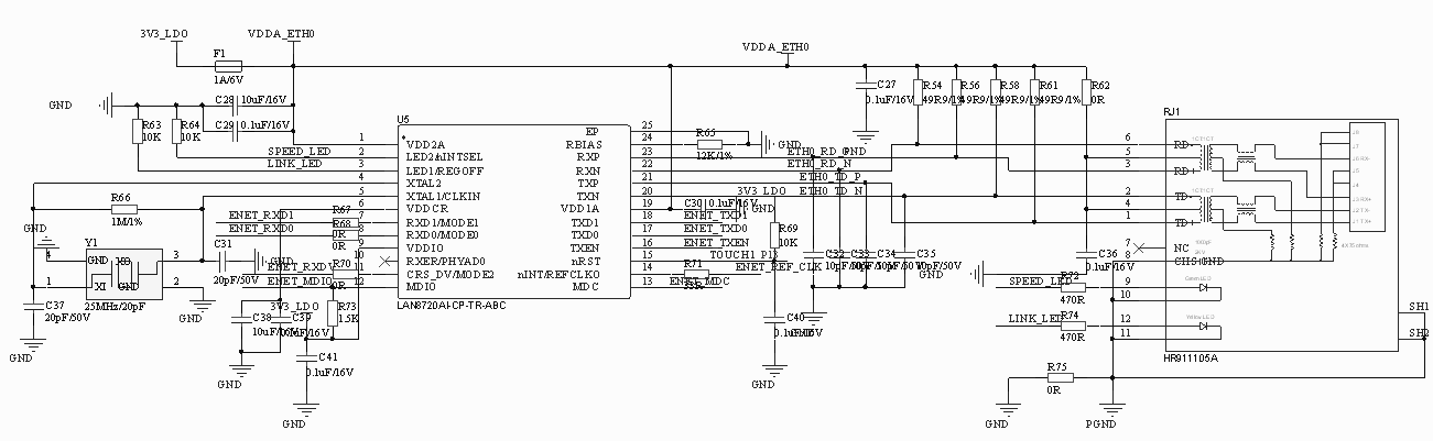
Ethernet
Pin description
| Pin No. | Signal | Feature |
|---|---|---|
| 41 | ENET_PHY_INT | GPIO27, interrupt signal |
| 42 | ENET_MDC | GPIO29, bus clock signal |
| 48 | ENET_RXD0 | GPIO33, data receiving signal, bit 0 |
| 49 | ENET_MDIO | GPIO32, management data input and output signals |
| 51 | ENET_RXD1 | GPIO34, data receiving signal, bit 1 |
| 52 | ENET_RXDV | GPIO35, data receiving valid signal |
| 56 | ENET_TXD0 | GPIO36, data sending signal, bit 0 |
| 57 | ENET_TXD1 | GPIO37, data sending signal, bit 1 |
| 63 | ENET_TXEN | GPIO38, data sending enable signal |
| 64 | ENET_REF_CLK | GPIO39, reference clock signal |
Applications
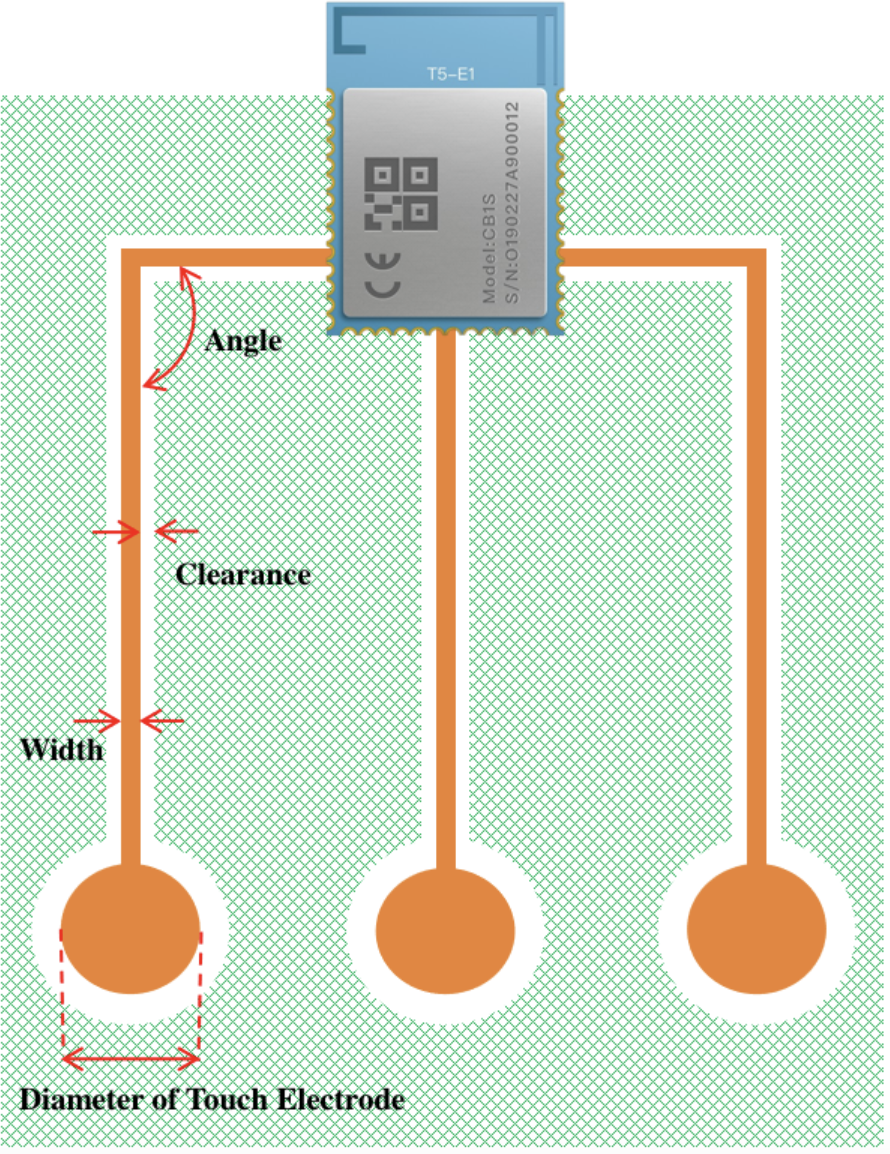
Touch
The T5-E1 module provides 16 capacitive sensing GPIOs, and the following table details the pins:
| Pin No. | Signal | Feature |
|---|---|---|
| 11 | P28 | TOUCH2 |
| 24 | P12 | TOUCH0 |
| 25 | P13 | TOUCH1 |
| 32 | P47 | TOUCH15 |
| 33 | P46 | TOUCH14 |
| 42 | P29 | TOUCH3 |
| 46 | P31 | TOUCH5 |
| 47 | P30 | TOUCH4 |
| 48 | P33 | TOUCH7 |
| 49 | P32 | TOUCH6 |
| 51 | P34 | TOUCH8 |
| 52 | P35 | TOUCH9 |
| 56 | P36 | TOUCH10 |
| 57 | P37 | TOUCH11 |
| 63 | P38 | TOUCH12 |
| 64 | P39 | TOUCH13 |
-
When using the touch feature, it is recommended to reserve a series resistor close to the module to reduce coupling noise and interference on the line and to enhance ESD protection. The recommended resistance value is 470 Ω to 2 kΩ, with 510 Ω preferred. The specific value depends on the actual test results of the product.
-
The traces should be as short and thin as possible, with a length less than 300 mm, a width no greater than 0.18 mm, and a trace angle greater than or equal to 90°. The spacing between different touch channels should be as far as possible, and they should be away from RF, I2C, SPI, and high-speed signal lines.
-
The touch electrodes and traces are surrounded by a grid ground, and the trace clearance from the ground ranges from 0.5 mm to 1 mm.
-
The diameter of the touch electrodes ranges from 8 mm to 15 mm.
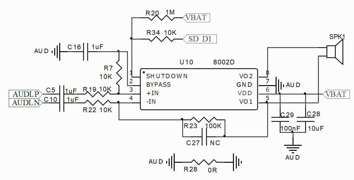
Speaker
Pin description
| Pin No. | Signal | Feature |
|---|---|---|
| 61 | LN | AUDL_N, audio negative output |
| 62 | LP | AUDL_P, audio positive output |
Applications
MIC
Pin description
| Pin No. | Signal | Feature |
|---|---|---|
| 66 | MP1 | MIC1_P, positive input of microphone 1 |
| 67 | MN1 | MIC1_N, negative input of microphone 1 |
| 68 | MN2 | MIC2_N, negative input of microphone 2 |
| 69 | MP2 | MIC2_P, positive input of microphone 2 |
| 70 | MBS | MICBIAS, microphone bias voltage |
Applications
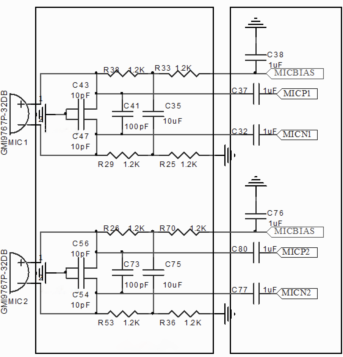
If only one MIC is used, MIC1 must be used.
Power supply
- The operating voltage range of T5-E1 is 2.5 V to 3.6 V. If you need to drive peripherals such as SD cards, 3.0 V to 3.6 V is recommended, with a typical value of 3.3 V. The 3.3 V supply current for the module should be greater than the maximum input current, and the total capacitance of external filter capacitors should be greater than 10 μF.
- Place the filter capacitors C1 and C2 near the power pin of the module.
Pins of the module
- The GPIO might experience an uncontrollable high level within five milliseconds of starting the module (before the program startup). Place a 4.7 kΩ pull-down resistor if needed.
- The RST pin of the module is a hardware reset pin. The module has internal weak pull-up resistors configured. If the pin is not used, it can float. If a module has been paired, this pin cannot be used to clear pairing information.
- The TX1 pin on the module is used to select a mode. Pulling TX1 down before the module is powered on will start the test firmware, while floating it or pulling it up will start the application firmware. In normal use, this pin is used as a log printing port.
- Other unused pins can be left floating.
- For more information about pin configuration, see the module datasheet.
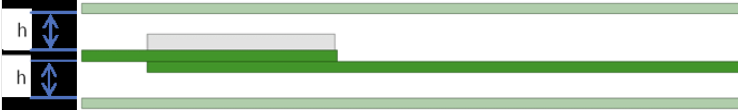
Power-on sequence of the module
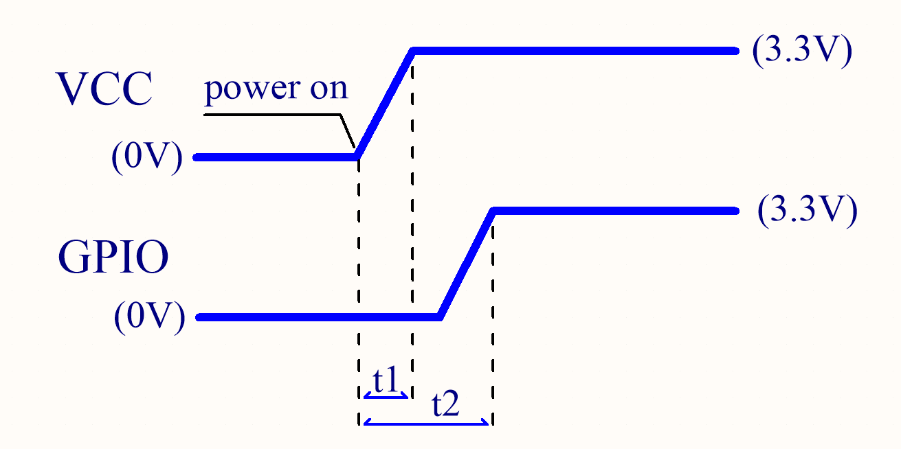
- Suppose that the high-level voltage settling time of the module’s GPIO is
t2and the voltage settling time of the module power pin ist1. Every time the module is powered on,t2must be greater than or equal tot1. As shown in the following figure:
-
If
t2is less thant1, the module might fail to start.- To return the module to its normal state, pull down the module reset pin (RST) for one millisecond and pull up to restart the module.
- Repeatedly power cycling the module power pin will not restore it to its normal state.
Low power design
Option 1: Control module power pin on/off
This circuit design can achieve overall low power consumption.
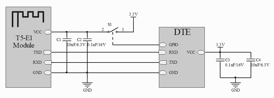
-
How it works: As shown in the circuit diagram, the MCU can control the switch
S1with the GPIO pin to power on/off the module.- When the MCU has data to report to the cloud, it turns the
S1on. Then, the module can receive data from the MCU and report data to the cloud and the mobile app. - When data reporting is completed, the module will be powered off and consume no power.
- When the MCU has data to report to the cloud, it turns the
-
Disadvantages:
- Current sinking occurs. When the switch
S1is turned off, the TXD and RXD pins on the module are still connected to the RXD and TXD pins on the MCU. - Therefore, the current from the MCU can flow into the VCC pin of the module through the UART pin.
- The TXD and RXD pins of the module are high, so the current sinking will increase the consumption of the module.
- When the switch
S1is turned on next time,t2will be less thant1, which can cause the module to be frozen.
- Current sinking occurs. When the switch
-
Solution 1: Optimize the software of the MCU without hardware modification. When the MCU detects the data reporting is completed, the program proceeds with the following steps.
- Set the TXD and RXD pins of the MCU as GPIO pins that are configured as the open-drain or weak pull-down mode.
- Turn the switch
S1off to power off the module. - This way, when the MCU has data to report, it turns the
S1on firstly. - Then, it configures the TXD and RXD pins as the UART to establish communication with the module for data transmission.
This solution does not apply to MCUs whose UART pin cannot be configured as the open-drain or weak pull-up mode. If the UART circuit has a pull-up resistor, one terminal of the resistor must be connected to the VCC pin of the module, or you can directly remove this resistor.
-
Solution 2: Add a level translator to the circuit without software modification. See the circuit diagram in the preceding sections Level translator reference and Connection between a module and a 3.3V MCU and embed a level translator in the UART circuit.
Option 2: Reduce power usage in idle state
Pull down the module’s RST pin to reduce idle consumption.
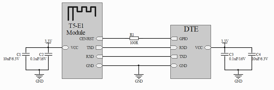
-
How it works: As shown in the circuit diagram, the MCU can control the RST pin with the GPIO pin to power on/off the module.
- When the MCU has data to report to the cloud, the GPIO outputs high to power on the module. Then, the module can receive data from the MCU and report data to the cloud and the mobile app.
- When data reporting is completed, the GPIO outputs low and the module runs in reset mode with low power consumption.
-
Disadvantage: The RST pin has a 10 kΩ internal pull-up resistor, so the module has an input current of 330 μA in the reset mode.
Radio frequency (RF) test
The antenna is susceptible to the distance from the shell to the surrounding components. We recommend that you test the RF performance after the final test. The RF test items and metrics are listed in the following table.
| Test item | Test metric |
|---|---|
| Increasing indoor distance | ≥ 50m |
| Increasing outdoor distance | ≥ 75m |
| Total radiated power (TRP) in the signaling mode of end devices (test mode of 11B 11 Mbit/s). | ≥ 10 dBm |
| Total isotropic sensitivity (TIS) in the signaling mode of end devices (test mode of 11B 11 Mbit/s). | ≤ -83 dBm |
- TRP and TIS must be tested in a dark chamber of the antenna manufacturers or certified organizations.
- The test items apply to most Wi-Fi products, excluding certain special products.
Antenna
Antenna clearance
-
Do not use metal shells or plastic shells with metallic paint or coating in the direction of the antenna radiation. Do not use metal objects such as screws and rivets near the antenna, which might affect the antenna efficiency. The distance between the antenna and other mental components should be at least 15 mm.
-
Try to increase the distance from the top shell to the antenna to minimize the impact on antenna performance.
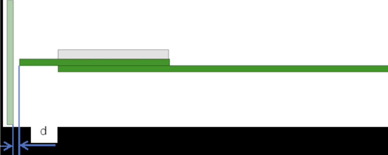
-
Try to increase the distance from the upper and bottom shells to the antenna to minimize the impact on antenna performance.
-
Keep the module away from speakers, power switches, cameras, HDMI, USB, and other high-speed signals to avoid interference.
-
Avoid metal shielding near the antenna. If co-channel interference occurs, you must evaluate the impact on the antenna performance and ensure isolation from interference.
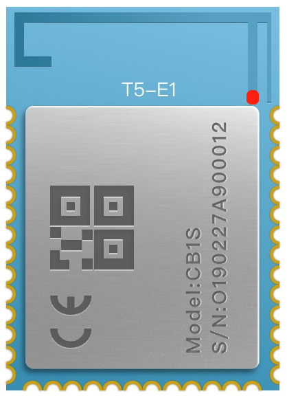
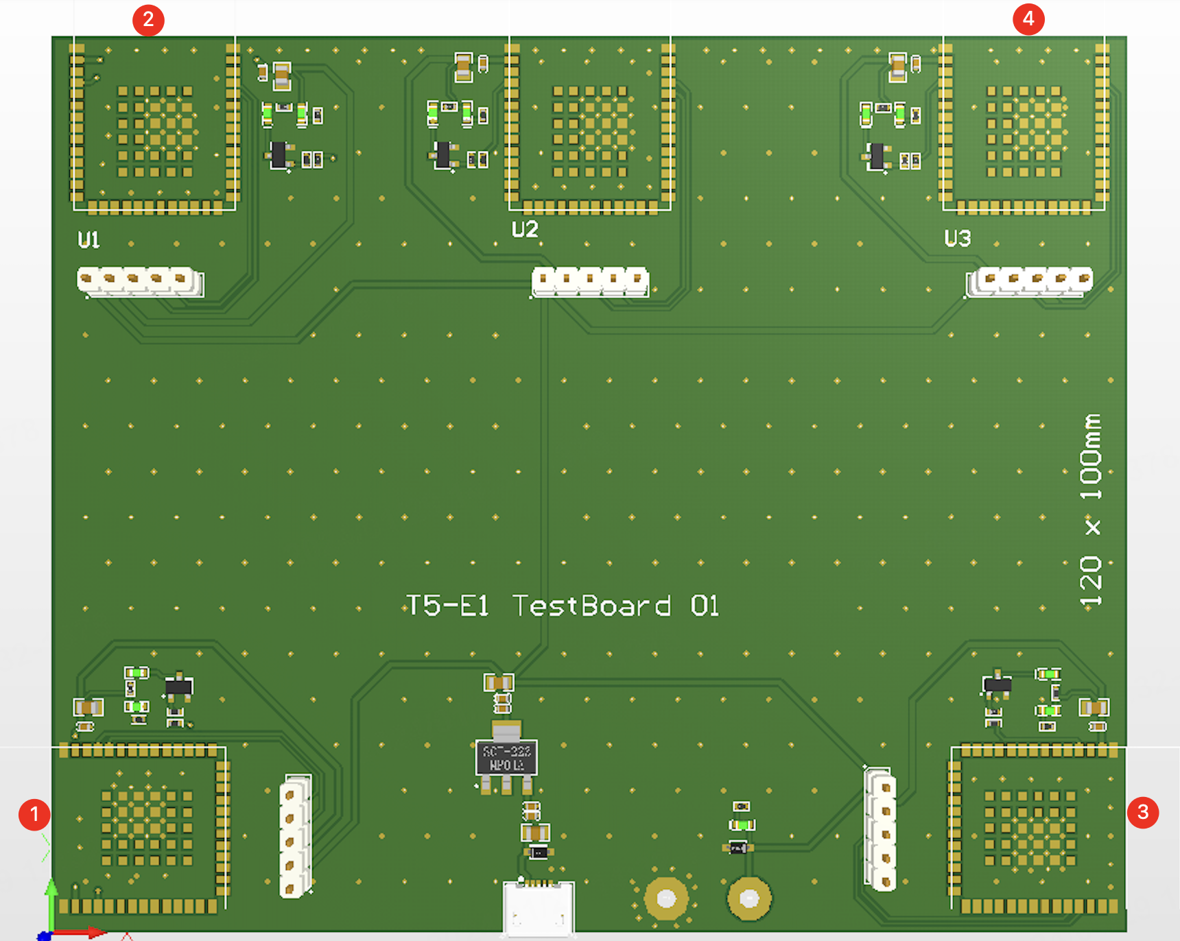
-
According to the antenna shape of the T5-E1 module, you can choose Position 3 or Position 4 (optimal) when using the module. That is to say, the antenna feed point should be as close to the edge of the board as possible. The position marked with a red dot in the figure below shows where the T5-E1 antenna feed point is.
Packing and manufacturing
Mechanical dimensions and backside pad dimensions
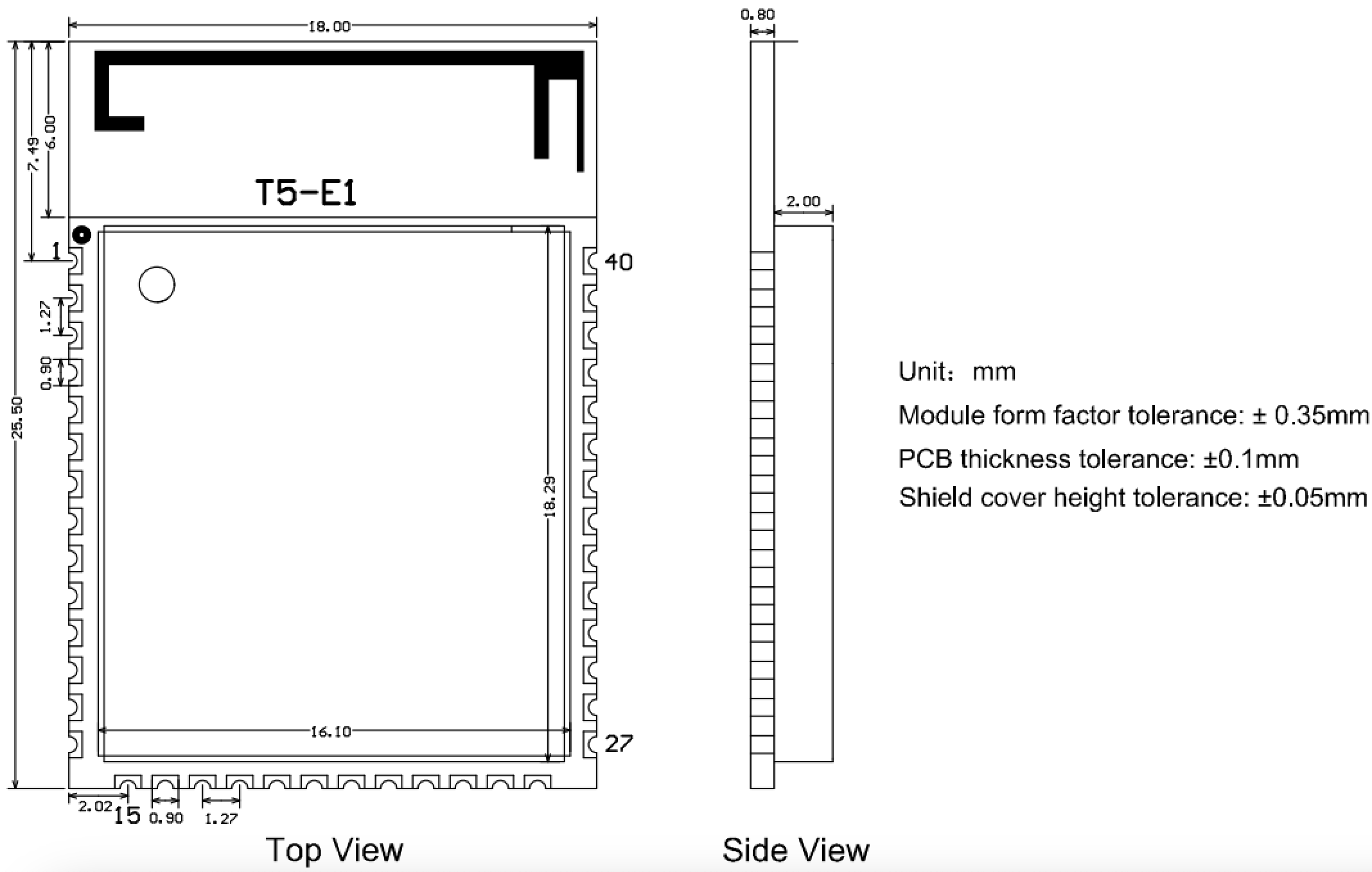
SMT package
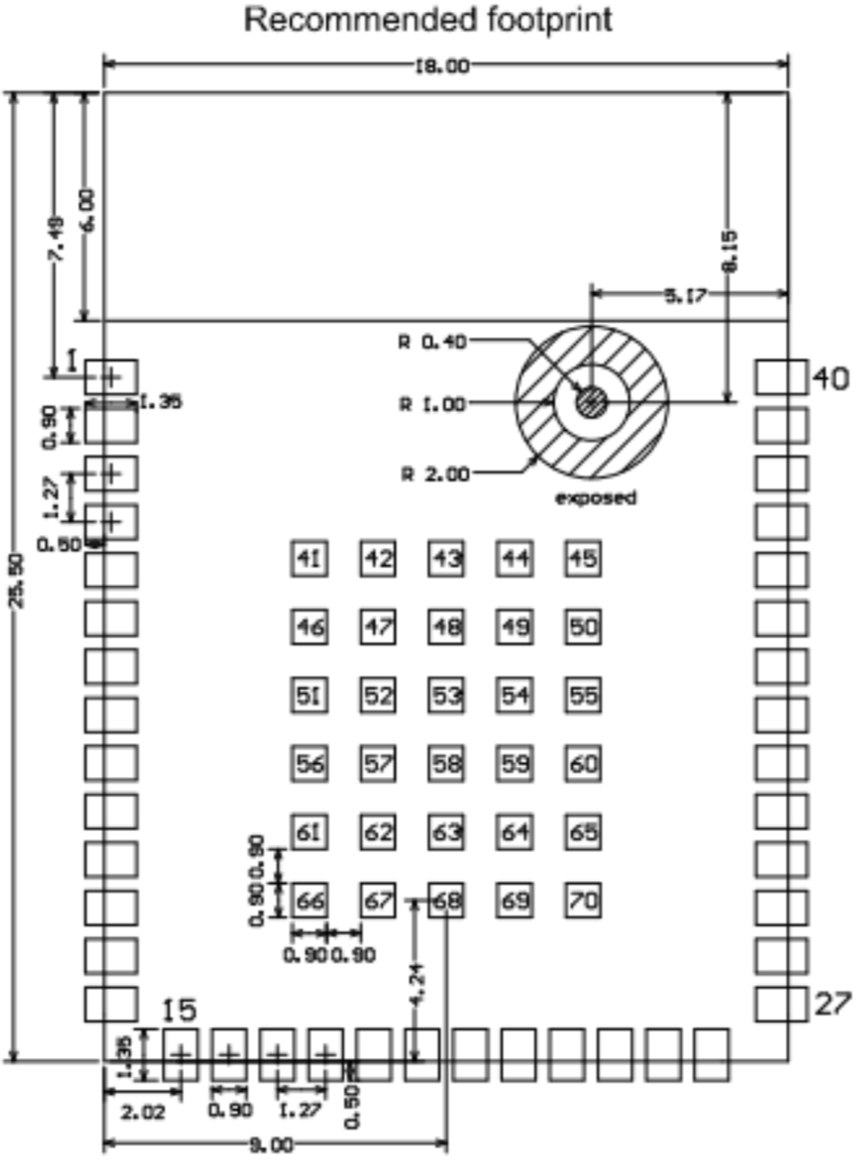
The tolerances for dimensions of length and width, height, and PCB thickness are ±0.35 mm, ±0.15 mm, and ±0.1 mm respectively.
Is this page helpful?
YesFeedbackIs this page helpful?
YesFeedback


