WBx Series Modules
This topic describes information about implementing serial communication between WBx series modules and MCUs.
Overview
WBx series is the Wi-Fi and Bluetooth Low Energy combo module developed by Tuya Smart. It consists of a highly integrated wireless RF chip BK7231T and a few peripheral components, with a built-in Wi-Fi network protocol stack and various library functions. It comes with a low-energy 32-bit MCU and 1T1R (1 transmitter/1 receiver) design. It provides output frequency up to 120 MHz, 256 KB embedded SRAM, 2 MB flash memory, and configurable GPIOs that can function as digital peripherals for various applications.
Serial communication protocol
Serial Communication Protocol
Serial Communication Protocol for Low Power Consumption
Serial Communication Protocol for HomeKit
Serial communication between module and MCU
-
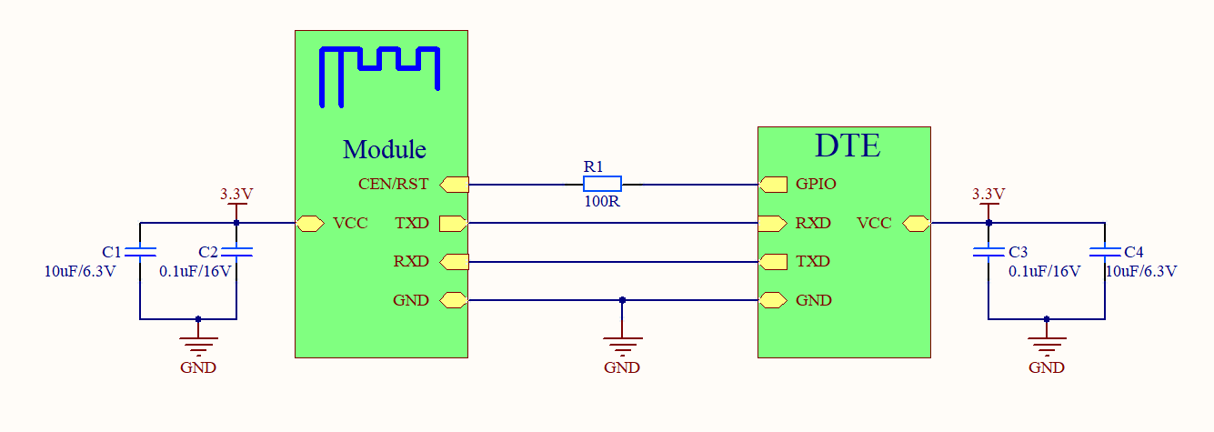
Connection between a module and a 3.3V MCU
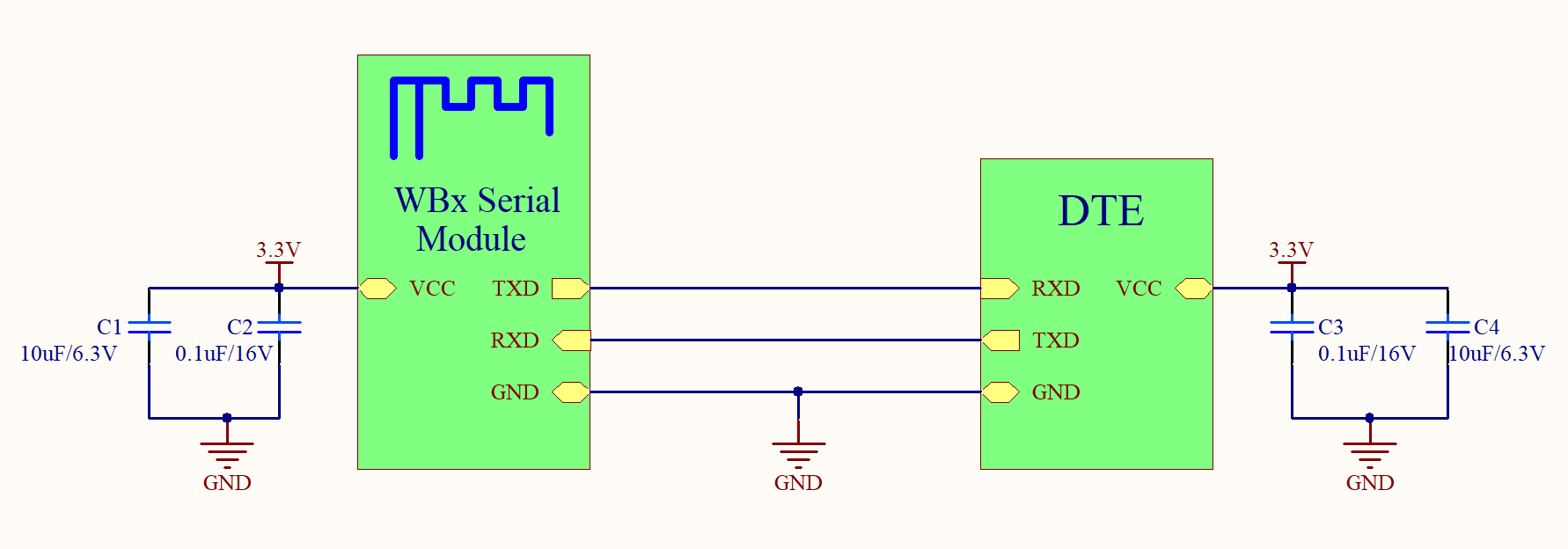
The VCC pin is the power pin of the module. The TXD and RXD pins are used for serial communication. The above schematic diagram does not apply to the WB1S module.
-
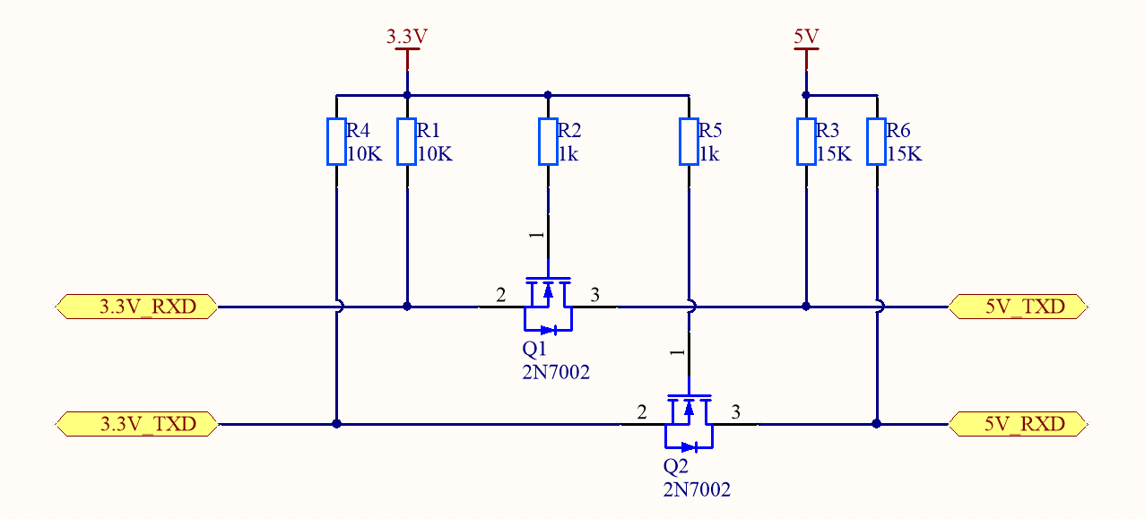
Connection between a module and a 5V MCU
In the following circuit diagram, voltage level translation can be implemented with a bidirectional voltage-level translator, a MOS transistor, or a triode.
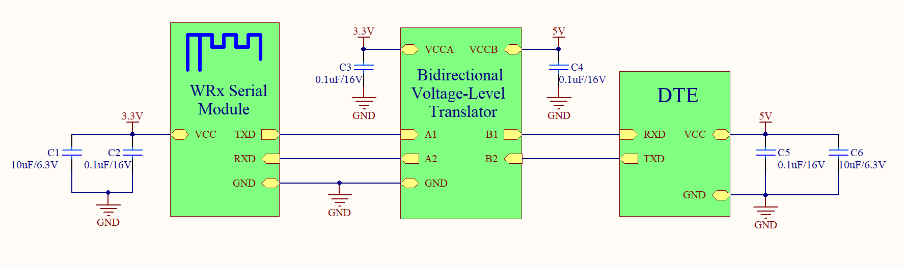
The VCC pin is the power pin of the module. The TXD and RXD pins are used for serial communication. The above schematic diagram does not apply to the WB1S module.
-
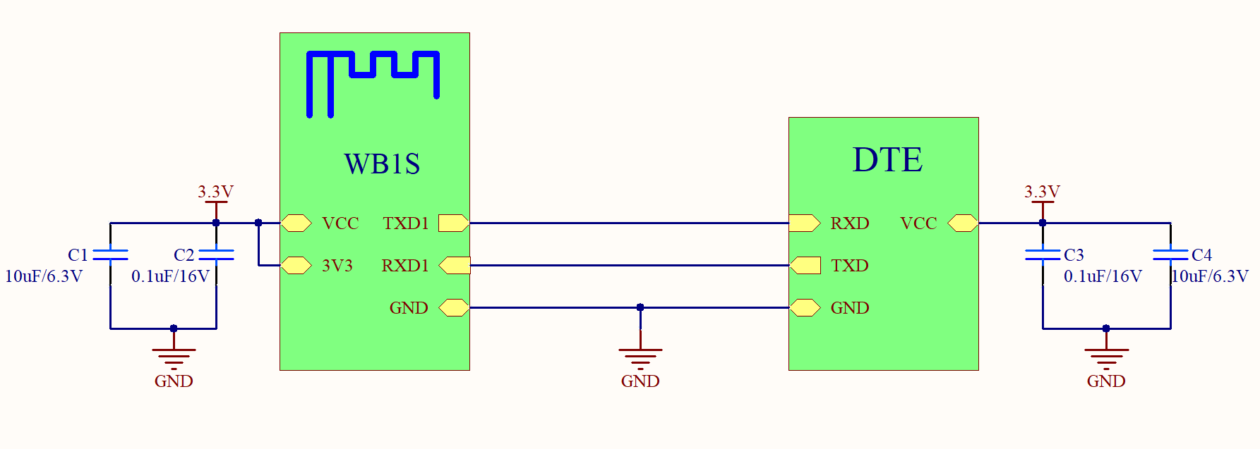
Connection between a WB1S and a 3.3V MCU
-
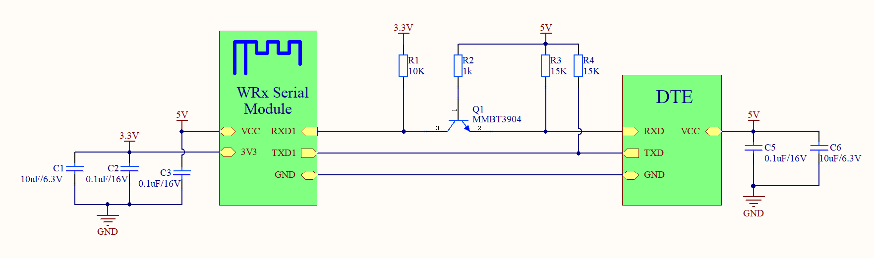
Connection between a WB1S and a 5V MCU
Level translator reference
-
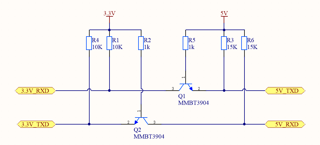
N-channel MOSFET level translator
In the following circuit diagram, an N-channel MOSFET and a built-in body diode are used to implement two-way communication.
-
NPN triode level translator
In the following circuit diagram, an NPN triode is used to implement one-way communication.
Design specification
-
The following table lists the specification and pin information of WRx modules for serial communication with an MCU.
Module model Input voltage (TYP) Input current (MAX) Power pin Power pin on silkscreen TXD pin TXD on silkscreen RXD pin RXD on silkscreen WB1S 3.3V 360 mA 4 3V3 2 TXD1 3 RXD1 WB2S 3.3V 430 mA 1 VBAT 7 TX 5 RX WB3S 3.3V 305 mA 8 VCC 16 TXD1 15 RXD1 WB3S-IPEX 3.3V 365 mA 8 VCC 16 TXD1 15 RXD1 WB3L 3.3V 402 mA 8 VCC 16 TXD1 15 RXD1 WB8P 3.3V 384 mA 1 VCC 9 TXD1 10 RXD1 -
Power supply
- Given that the supply current for 3.3V modules must be greater than the maximum input current, a supply current of at least 500 mA is recommended. The total capacity of the external filter capacitor must not be less than 10 μF.
- Place the filter capacitors C1 and C2 near the power pin of the module.
-
Pins of the module
- The reset pin or enable pin of the module is a hardware reset pin. The module has internal weak pull-up resistors configured. If the pin is not used, it can float. If a module has been paired, this pin cannot be used to clear pairing information.
- When pin initialization is in progress after a system reboot, the user UART is in a high impedance state.
- Other unused pins can float.
- For more information about the pin definition, see the datasheet of each module.
-
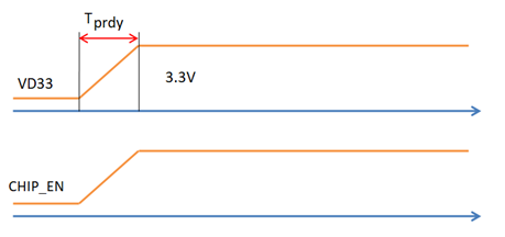
Power-on sequence of the module
-
Every time a module is powered on, the voltage ready time is not greater than 5 ms.
-
-
Auto-baud detection firmware
- To detect the baud rate of the MCU, the program will turn on and off the UART peripheral several times. When UART is turned off, its TX and RX pins will be in a high impedance state. If you plan to use a level translator circuit, make sure the signal lines remain the level in idle state when the TX and RX pins are high impedance.
-
Antenna clearance
-
Do not use metal shells or plastic shells with metallic paint or coating in the direction of the antenna radiation. Do not use metal objects such as screws and rivets near the antenna, which might affect the antenna efficiency.
-
Try to increase the distance from the top shell to the antenna to minimize the impact on antenna performance.
-
Try to increase the distance from the upper and bottom shells to the antenna to minimize the impact on antenna performance.
-
Keep the module away from speakers, power switches, cameras, HDMI, USB, and other high-speed signals to avoid interference.
-
Avoid metal shielding near the antenna. If co-channel interference occurs, you must evaluate the impact on the antenna performance and ensure the isolation from interference.
-
-
Placement
-
Horizontal placement
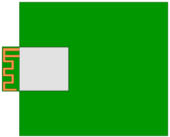
We recommend that you place the module at the edge of the backplane with the antenna facing outward, and flush the module’s GND terminal with the backplane’s GND terminal. Both terminals are fully connected.
-
Embedded placement
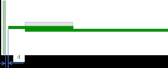
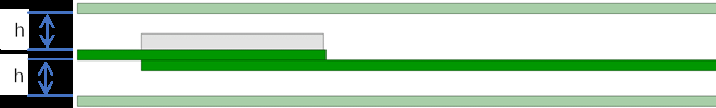
Embed the module into the backplane through a slot that is flushed with or deeper than the module’s GND terminal. The side of the slot must be 15 mm or farther from the module’s board edge.
A wider slot can achieve better performance that is still weaker than that of horizontal placement.
-
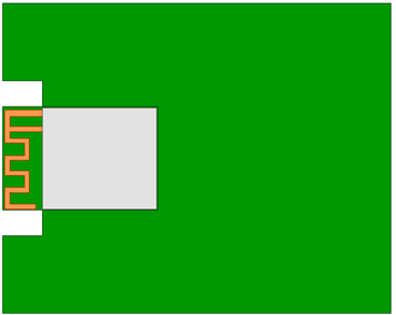
Vertical placement
Insert the module vertically into the backplane slot with the antenna facing upward. The module’s GND terminal and the backplane’s GND terminal must be fully connected. We recommend that you keep a clearance distance of 15 mm or more around the antenna.
-
Low power design considerations
Control the on/off condition of the module to achieve overall low power consumption.
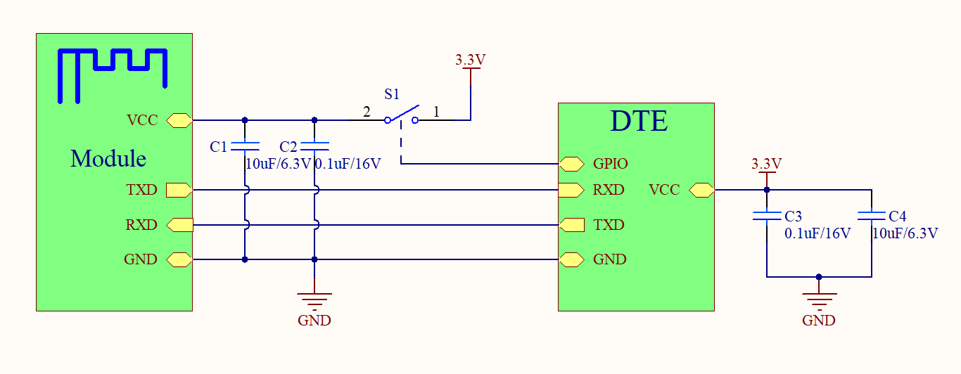
As shown in the circuit diagram, the MCU can control the switch S1 with the GPIO pin to power on/off the module. When the MCU has data to report to the cloud, it turns the S1 on. Then, the module can receive data from the MCU and report data to the cloud and the client. When data reporting is completed, the module will be powered off and consume no power.
Disadvantages
Current sinking occurs. When the switch S1 is turned off, the current from the MCU can flow into the VCC pin of the module through the UART pin because the TXD and RXD pins of the MCU and the module are still connected. The TXD and RXD pins of the module are high so the current sinking will increase the consumption of the module. This might also cause the module to not operate correctly.
Solution 1
Optimize the software of the MCU without hardware modification.
When the MCU detects the data reporting is completed, the program proceeds with the following steps.
-
Set the TXD and RXD pins of the MCU as GPIO pins that are configured as the open-drain or weak pull-down mode.
-
Turn the switch
S1off to power off the module. -
This way, when the MCU has data to report, it turns the
S1on firstly. -
Then, it configures the TXD and RXD pins as the UART to establish communication with the module for data transmission.
This solution does not apply to MCUs whose UART pin cannot be configured as the open-drain or weak pull-up mode. If the UART circuit has a pull-up resistor, one terminal of the resistor must be connected to the VCC pin of the module, or you can directly remove this resistor.
Solution 2
Add a level translator to the circuit without software modification. See the circuit diagram in the sections Level translator reference and Connection between a module and a 3.3V MCU and embed a level translator in the UART circuit.
Pull down the module’s clock enable (CEN) pin or reset (RST) pin to reduce the idle consumption.
As shown in the circuit diagram, the MCU can control the CEN or RST pin with the GPIO pin to power on/off the module. When the MCU has data to report to the cloud, the GPIO outputs high to power on the module. Then, the module can receive data from the MCU and report data to the cloud and the client. When data reporting is completed, the GPIO outputs low and the module runs in reset mode with low power consumption.
Disadvantages
If the CEN or RST pin has an internal pull-up resistor, when the module runs in reset mode, this resistor can consume power.
RF test items and metrics
The antenna is susceptible to the distance from the shell to the surrounding components. We recommend that you test the radio frequency (RF) performance after the final test. The RF test items and metrics are listed in the following table.
| No. | Test item | Test metric |
|---|---|---|
| 1 | Increasing indoor distance | ≥ 25 m |
| 2 | Increasing outdoor distance | ≥ 75m |
| 3 | Total radiated power (TRP) in the signaling mode of end devices (test mode of 11B 1 Mbit/s). | ≥ 10 dBm |
| 4 | Total isotropic sensitivity (TIS) of end devices | ≤ -62 dBm |
- Items 3 and 4 must be tested in a dark chamber of the antenna manufacturers or certified organizations.
- The test items apply to most Wi-Fi products, excluding certain special products.
Is this page helpful?
YesFeedbackIs this page helpful?
YesFeedback


