BK3432 Module Datasheet
Product overview
With the data rate of 2 Mbit/s, the BK3432 chip is a highly integrated Bluetooth 5.0 dual-mode data SoC. It’s integrated with a high-performance RF transceiver, baseband, MCU, rich feature peripherals, and the programmable protocol and profile, to support Bluetooth classic and low energy applications. The flash memory enables BK3432 to work for customized applications.
The BK3432 is designed with the advanced technological process and integrated with a switch DCDC regulator so that it has ultra-low power consumption and ultra-low leakage power. Embedded with the high order interference suppression filter and fast automatic gain control logic, the BK3432 can work well in the environment of high interference.
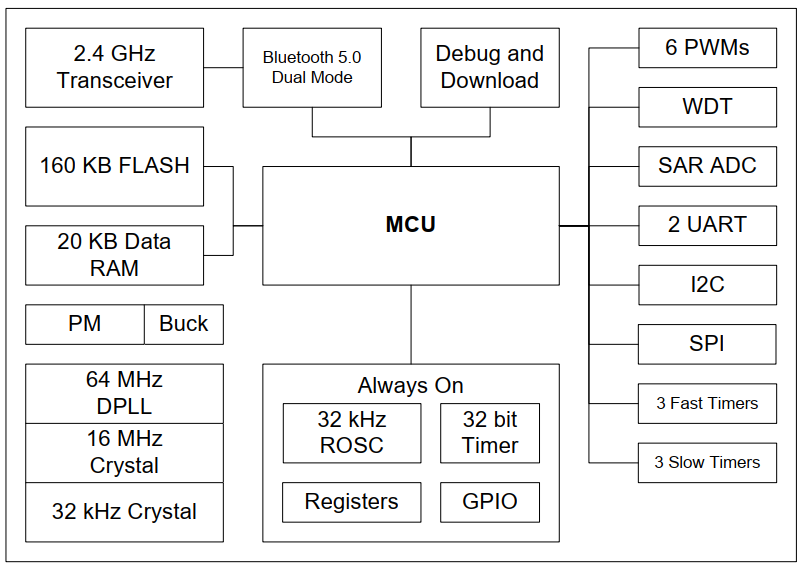
The following figure shows the BK3432 block chip:
Features
- Bluetooth® SIG Bluetooth dual-mode 5.0 compliant
- Low-power 2.4GHz Transceiver
- MCU integrated
- 160 KB programmable flash for programs and 20 KB RAM for data
- Program code read protection
- The voltage is from 0.9 V to 3.6 V
- Clock:
- 16 MHz crystal reference clock
- 64 MHz digital PLL clock
- 32 kHz ring oscillator
- External 32 kHz crystal oscillator
- MCU can run with any clock source with internal frequency divider
- Interface and peripheral units:
- JTAG, I2C, and SPI interfaces
- Two UARTs
- Multi-channel PWM output
- On-chip 10-bit general ADC
- GPIO with multiplexed interface functions
- True random number generator
- Package type:
- 32-pin QFN 4x4
Pin information
QFN32
The following figure shows pins of the BK3432 QFN32.
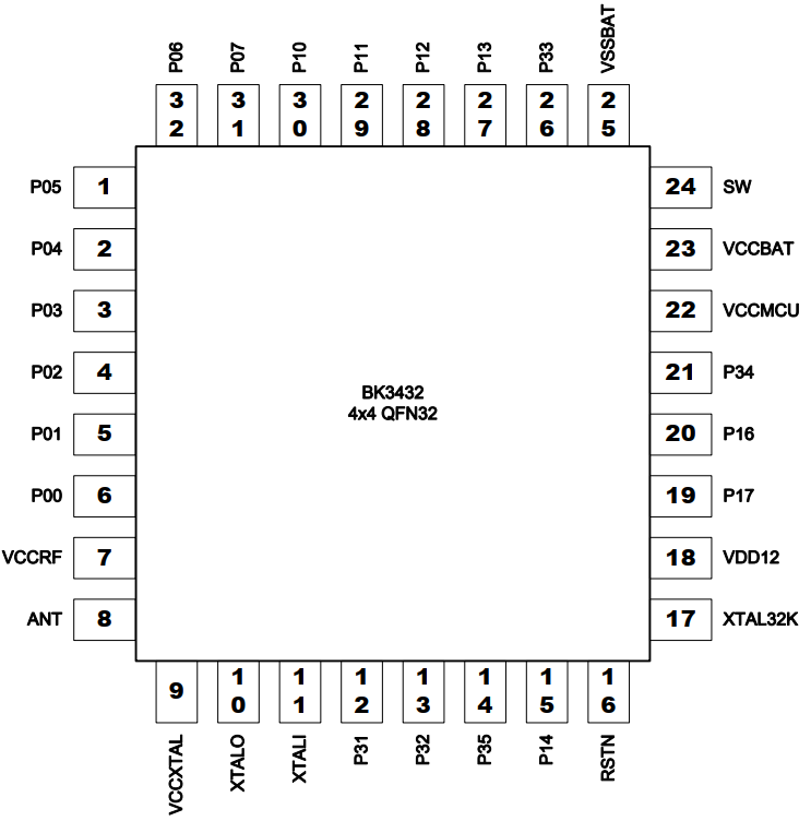
The following table gives detailed information about pins of the BK3432 QFN32.
| Serial number | Pin name | Function | Description |
|---|---|---|---|
| 1 | P05 | Digital I/O | General purpose I/O |
| 2 | P04 | Digital I/O | General purpose I/O |
| 3 | P03 | Digital I/O | General purpose I/O |
| 4 | P02 | Digital I/O | General purpose I/O |
| 5 | P01 | Digital I/O | General purpose I/O |
| 6 | P00 | Digital I/O | General purpose I/O |
| 7 | VCCRF | Power | RF power, 1.5 V |
| 8 | ANT | RF | RF signal port |
| 9 | VCCXTAL | Power | Crystal power, 1.5 V |
| 10 | XTALO | Analog | 16 MHz crystal output |
| 11 | XTALI | Analog | 16 MHz crystal input |
| 12 | P31 | Digital I/O | General purpose I/O |
| 13 | P32 | Digital I/O | General purpose I/O |
| 14 | P35 | Digital I/O | General purpose I/O |
| 15 | P14 | Digital I/O | General purpose I/O |
| 16 | RSTN | Analog | Active low, reset pin |
| 17 | XTAL32K | Analog | 32 kHz Crystal input |
| 18 | VDD12 | Analog | LDO output, 1.5 V |
| 19 | P17 | Digital I/O | General purpose I/O |
| 20 | P16 | Digital I/O | General purpose I/O |
| 21 | P34 | Digital I/O | General purpose I/O |
| 22 | VCCMCU | Power | Power, 1.5 |
| 23 | VCCBAT | Analog | Power, 3 V |
| 24 | SW | Analog | Switch regulator pin in the two battery mode |
| 25 | VSSBAT | Analog | Ground |
| 26 | P33 | Digital I/O | General purpose I/O |
| 27 | P13 | Digital I/O | General purpose I/O |
| 28 | P12 | Digital I/O | General purpose I/O |
| 29 | P11 | Digital I/O | General purpose I/O |
| 30 | P10 | Digital I/O | General purpose I/O |
| 31 | P07 | Digital I/O | General purpose I/O |
| 32 | P06 | Digital I/O | General purpose I/O |
Functional description
GPIO
The BK3432 QFN32 has 20 GPIO pins in total. The pins can be configured to be input or output. There are secondary functions available to GPIO pins and configurable by firmware.
At the startup, which mode (programming mode, JTAG mode or normal mode) the chip enters depends on the received command from the mode selecting pin.
The following table describes the functional mapping of GPIO of BK3432.
| Pin number | Description | I/O type | Program mode | Mode selection pin | JTAG mode |
|---|---|---|---|---|---|
| P00 | UART_TX | O | |||
| P01 | UART_RX | I | |||
| P02 | I2C_SCL | I/O | |||
| P03 | I2C_SDA | I/O | JTAG_NTRST | ||
| P04 | SPI_SCK | I/O | SPI_MOSI | SPI_MOSI | JTAG_TDI |
| P05 | SPI_MOSI | I/O | SPI_MISO | SPI_MISO | JTAG_TDO |
| P06 | SPI_MISO/PWM[4] | I/O | SPI_SCK | SPI_SCK | JTAG_TCK |
| P07 | SPI_NSS/PWM[5] | I/O | SPI_CS | SPI_CS | JTAG_TMS |
| P10 | PWM[0] (20mA) | O | |||
| P11 | PWM[1] (20mA) | O | |||
| P12 | PWM[2] | O | |||
| P13 | PWM[3] | O | |||
| P14 | PWM[4] | ||||
| P16 | UART2_TX | O | |||
| P17 | UART2_RX | O | |||
| P31 | Ch1 | I | |||
| P32 | Ch2 | I | |||
| P33 | Ch3 | ||||
| P34 | Ch4 | I | |||
| P35 | Ch5 | I |
Note: Each GPIO pin can wake up an MCU in the shutdown state. In the shutdown state, any change in voltage and level of the pre-configured GPIO pin will trigger the wake-up procedure.
Timers
-
PWM timers
There are six 16-bit PWM timers. The clock of PWM timers can be 32 KHz or 16 MHz.
There are two modes for a PWM timer: timer mode and PWM mode. In the timer mode, MCU can be interrupted. In the PWM mode, PWM waveforms can be generated and output to GPIO pins to drive external devices such as LED. Six GPIO pins can be used to output PWM waveforms separately.
-
Dog watching timer and RTC timer
The dog watching timer and RTC timer run in the always-on-power domain, whose clock rate is 32 kHz.
The 16-bit dog watching timer runs in the frequency of 4 kHz. Its period can be up to 16 second. After the dog watching timer expires, it will reset the whole chip.
The 32-bit RTC timer in the always-on-power domain runs in the ROSC frequency. Its period can be up to one day. After an RTC timer expires, it will wake up the MCU.
ADC
A 10-bit generic ADC is integrated into BK3432. There are 5 external channels and 1 internal channel selected for transferring of an ADC. The ADC supports both single and continuous modes.
| ADC channel number | ADC source |
|---|---|
| Channel 1 | GPIO 31 |
| Channel 2 | GPIO 32 |
| Channel 3 | GPIO 33 |
| Channel 4 | GPIO 34 |
| Channel 5 | GPIO 35 |
| Channel 7 | VCCBAT-pin |
UART, I2C, and SPI
There are two sets of UARTs, and one set is I2Cs and the other set are SPI interfaces. All of them support both master and slave modes.
The UART baud rate can be up to 3.2 MHz and the SPI clock rate can be up to 4 MHz.
Security
A generator produces a random number to make the system get better security communication.
Content of the flash will be protected (not readable, but erasable) as long as the LSB Bit 3 or 5 of the last 32-bit word of the last address 0x9FFF is set to 0.
Electrical specifications
The following table describes RF characteristics of BK3432:
| Name | Parameter (Condition) | Minimum value | Typical value | Maximum value | Unit | Comment |
|---|---|---|---|---|---|---|
| VCC | Voltage | 0.9 | 3.0 | 3.6 | V | |
| TEMP | Temperature | -40 | +27 | +125 | ºC | |
| VIH | High level | VCC-0.3 | VCC+0.3 | V | ||
| VIL | Low level | VSS | VSS+0.3 | V | ||
| VOH | High level (IOH=-0.25mA) | VCC- 0.3 | VCC | V | ||
| VOL | Low level(IOL=0.25mA) | VSS | VSS+0.3 | V | ||
| IVDD | Deep sleep | 0.5 | uA | |||
| IVDD | Sleep current (RF OFF,32kHz clock,DIG Retention | 1.8 | uA | |||
| IVDD | Active RX (3.3 V) | 5.1 | mA | With DCDC regulator | ||
| IVDD | Active TX @ -1 dBm (3.3V) | 4.8 | mA | With DCDC regulator | ||
| FOP | Operating frequency | 2400 | 2480 | MHz | ||
| FXTAL | Crystal frequency | 16 | MHz | |||
| RFSK | Air data rate | 1 | 2 | Mbps | ||
| PRF | Output power | -20 | -1 | +4 | dBm | |
| PBW | Modulation 20 dB bandwidth | 1 | MHz | |||
| PRF1 | Out of band emission 2 MHz | -20 | dB | |||
| PRF2 | Out of band emission 3 MHz | -58 | dB | |||
| Dev | Transmit FM deviation | 115 | 250 | 300 | kHz | |
| Drift | Transmit drift in any position | 400 | Hz/us | |||
| Max Input | 1 E-3 BER | -10 | dBm | |||
| RXSENS | 1 E-3 BER sensitivity | -96 | -97 | dBm | ||
| Intermo dulation | Pin=-64 dBm; Punwant=- 50 dBm; f0=2f1-f2, f2- f1=3, 4 or 5MHz | -25 | -22 | dBm | ||
| C/ICO | Co-channel C/I | 7 | dB | |||
| C/I1ST | ACS C/I 1MHz | -9 | -6 | dB | ||
| C/I2ND | ACS C/I 2MHz | -44 | dB | |||
| C/I3RD | ACS C/I 3MHz | -50 | dB | |||
| C/I1STI | ACS C/I Image channel | -25 | dB | |||
| C/I2NDI | ACS C/I 1 MHz | -35 | dB | |||
| Block | Block @ 2399 and 2484 | -15 | dBm | |||
| Block | Block @ 2 GHz and 3 GHz | -15 | dBm | |||
| Leakage | Leakage @ < 1GHz | -71 | dBm | |||
| Leakage | Leakage @ >1GHz | -56 | dBm |
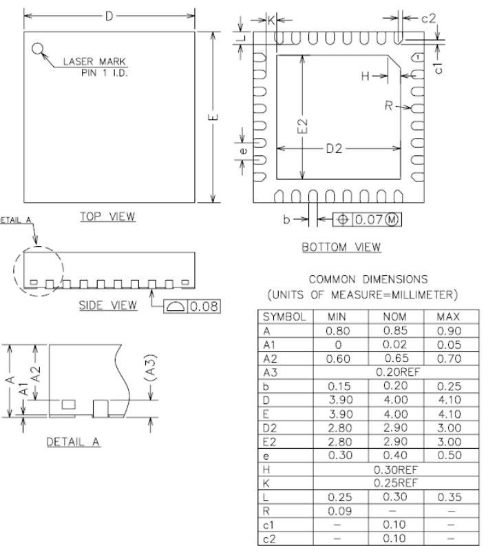
Package information
The BK3432 uses the QFN package of 4 mmx4 mm.
Order information
| Part number | Package | Shipping packing method | Minimum order quantity |
|---|---|---|---|
| BK3432QN32C | QFN 4mmx4mm 32-Pin | Tape Reel | 3000 |
Revision history
| Version | Date | Description |
|---|---|---|
| 0.1 | Mar 12, 2017 | This is the first release. |
| 0.2 | Nov 11, 2018 | Modified the order information. |
Is this page helpful?
YesFeedbackIs this page helpful?
YesFeedback


