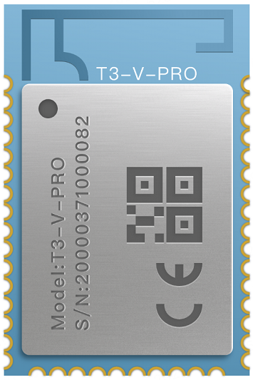
T3-V-PRO Modules
This topic is intended to provide hardware information and serve as a reference when you develop with T3-V-PRO modules. It helps you get an overall understanding of the product specifications and assists in developing products and applications.
Interface description
The T3-V-PRO module features a built-in Wi-Fi and Bluetooth LE wireless chip, a voice chip, one SPK circuit (with built-in power amplifier), one MIC circuit, and one acoustic echo cancellation (AEC) loopback circuit. Support major AI models including Doubao, DeepSeek, Qwen, OpenAI, and Gemini, featuring button wake-up, wake-word activation, and free conversation capabilities. This module delivers vivid and engaging AI voice interaction experiences, making it ideally suited for AI smart toys and similar products.
The module provides three UART interfaces:
-
Flashing UART: used to connect to your MCU. The serial data transmission follows Tuya’s protocol. The baud rate is 115200 bps by default.
-
Logging UART: the logging serial port of the main chip.
-
Voice chip UART: The serial port used for flashing firmware to the voice chip.
Pin No. Signal Functional description 7 TX0 Serial port 0 for sending data. It can be used as a download port or for MCU general integration. 8 RX0 Serial port 0 for receiving data. It can be used as a download port or for MCU general integration. 4 TX1 Serial port 1 for sending data. Logging serial port. 5 RX1 Serial port 1 for receiving data. Logging serial port. 10 CI_TX0 Serial port for sending data, and the flashing port of the voice chip. 11 CI_RX0 Serial port for receiving data, and the flashing port of the voice chip.
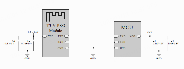
Serial communication between module and MCU
-
Connection between a module and a 3.3V MCU
-
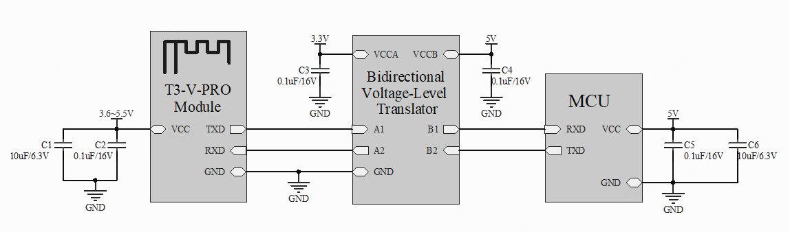
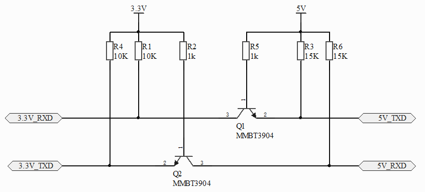
Connection between a module and a 5V MCU In the following circuit diagram, voltage level translation can be implemented with a bidirectional voltage-level translator, a MOS transistor, or a triode.
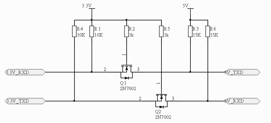
Level translator reference
-
N-channel MOSFET level translator: An N-channel MOSFET and a built-in body diode are used to implement two-way communication.
-
NPN triode level translator: An NPN triode is used to implement one-way communication.
Circuit design
The UART trace should be as short as possible. Add ground vias around the UART and keep away from RF and periodic signal lines.
The T3-V-PRO module has one set of SPI interfaces, and the following table details the pins:
| Pin No. | Signal | Functional description |
|---|---|---|
| 33 | SPI_CSN | GPIO15, SPI chip select signal |
| 34 | SPI_MISO | GPIO17, SPI controller in and agent out |
| 35 | SPI_SCK | GPIO14, SPI clock signal |
| 36 | SPI_MOSI | GPIO16, SPI controller out and agent in |
Electrical specifications and applications
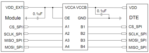
The voltage level of the SPI interface on this module is 3.3V. A level translator should be used if the application is equipped with a 5V UART interface. A level translator for SPI is recommended. The reference circuit is shown in the figure below:
Schematic diagrams
Things to note
Antenna clearance
- Do not use metal shells or plastic shells with metallic painting or coating in the direction of the antenna radiation. Do not use metal objects such as screws and rivets near the antenna, which might affect the antenna efficiency.
- Try to increase the distance from the top shell to the antenna to minimize the impact on antenna performance.
- Try to increase the distance from the upper and bottom shells to the antenna to minimize the impact on antenna performance.
- Keep the module away from speakers, power switches, cameras, HDMI, USB, and other high-speed signals to avoid interference.
- Avoid metal shielding near the antenna. If co-channel interference occurs, you must evaluate the impact on the antenna performance and ensure isolation from interference.
Antenna placement
- Horizontal placement
We recommend that you place the module at the edge of the backplane with the antenna facing outward, and flush the module’s GND terminal with the backplane’s GND terminal. Both terminals are fully connected. - Embedded placement
Embed the module into the backplane through a slot that is flushed with or deeper than the module’s GND terminal. The side of the slot must be 15 mm or farther from the module’s board edge. A wider slot can help achieve better performance, but it is weaker than that of horizontal placement. - Vertical placement
Insert the module vertically into the backplane slot with the antenna facing upward. The module’s GND terminal and the backplane’s GND terminal must be fully connected. We recommend that you keep a clearance distance of 15 mm or more around the antenna.
Selection and design solutions of the microphone and speaker
-
Microphone selection
- Acoustic technical indicators reference:
- Analog microphone: Sensitivity ≥ -38 dBV, SNR ≥ 62 dB, THD ≤ 1%, and AOP ≥ 120 dB SPL.
- Digital microphone: Sensitivity = -26±2 dBFS, SNR ≥ 62 dB, THD ≤ 1%, and AOP ≥ 120 dB SPL.
- Recommend prioritizing MEMS microphones (superior SNR, consistency, and reliability).
- The frequency response of the microphone should be kept as flat as possible within the range of 100 Hz to 8 kHz, with a fluctuation of ≤ 3 dB.
- Phase consistency shall be ≤ 5° within the 100 Hz to 4 kHz frequency range, and ≤ 10° within the 4 kHz to 8 kHz frequency range.
- Acoustic technical indicators reference:
-
Speaker selection
- Total harmonic distortion (THD) of the speaker:
- 100 Hz to 200 Hz: THD < 8%.
- 200 Hz to 400 Hz: THD < 5%.
- 400 Hz to 8 kHz: THD < 3%.
- Total harmonic distortion (THD) of the speaker:
-
Audio loopback and PA design guidelines
- The echo reference signal should be sampled close to the speaker side, specifically at the power amplifier (PA) output. The T3-V-PRO module has a built-in PA and loopback circuit.
- At maximum speaker volume, the echo reference signal input to the microphone must not saturate or distort. PA output THD at maximum volume shall be ≤ 1% within the 100 Hz to 10 kHz range.
- THD of the speaker at maximum volume:
- 100 Hz to 200 Hz: THD < 8%.
- 200 Hz to 400 Hz: THD < 5%.
- 400 Hz to 8 kHz: THD < 3%.
- At maximum volume, the sound pressure level (SPL) at the microphone must not exceed 102 dB @1 kHz.
- During peak playback, the loopback signal level should be between -3 dB and -6 dB.
-
AEC effect verification
- Dump 3 channels of audio (1 channel microphone, AFE loopback, and audio after AEC), then use audio tool software to check whether the audio has saturation, data loss, and other issues.
-
Microphone cavity design
- The inner diameter (ID) of the microphone pickup hole on the housing shall be > 0.8 mm.
- The hole length should be as short as possible, while the diameter should be as large as possible, with an aspect ratio (diameter to depth) ≥ 1:3.
- The microphone must be kept away from interference sources (such as cooling fans) or vibration sources (such as speaker vibrations or structural vibrations). Moreover, the microphone is sealed with a silicone cover and a solid surface to reduce housing vibration and sound transmission.
- Choose the softest possible silicone cover to minimize vibration between the microphone and mold.
- Avoid front cavity designs where both ends are smaller than the middle section to prevent forming resonant chambers.
-
Microphone and speaker layout considerations
- The entire device cavity must maintain proper sealing to ensure microphone recording remains unaffected by internal speaker playback vibrations and echo feedback.
- The speaker must have an independent acoustic chamber, with complete isolation from the microphone chamber. Any structural gaps should be sealed with foam or adhesive.
- The microphone pickup hole and speaker output ports should not face the same plane – ideally oriented at 90° or greater relative to each other.
- Maximize the distance between the speaker output and the microphone input. A minimum 100 mm separation is recommended where possible.
- A silicone cover or foam can be applied between the microphone and device housing to enhance sealing and vibration damping.
PCB layout
- Ensure power traces are short and wide, with minimal loops, and provide at least two 12 mil (inner diameter) vias for main IC power pins.
- For power traces, use copper pours whenever possible and add sufficient ground vias for heat dissipation. Pay attention to the current-carrying capacity of single traces. The T3-V-PRO module is designed for a maximum current of 1A. Trace width reference (1 oz copper, outer layer): 20 mil width corresponds to 1A (without considering temperature rise).
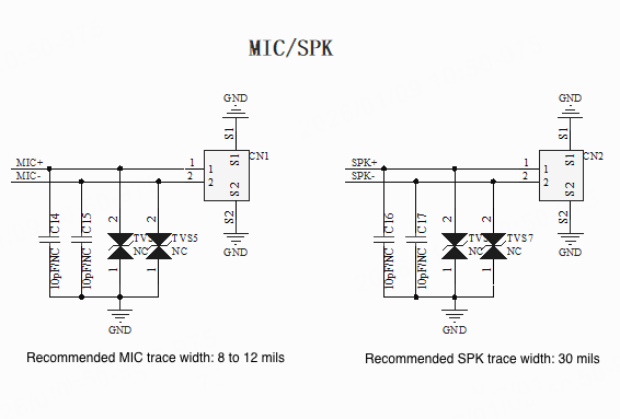
- The module’s audio output signals, SPK+ and SPK-, must be routed as differential pairs and fully ground-guarded. The traces should be as short as possible. Trace width should be calculated based on peak output current, and a minimum of 30 mil is recommended.
- The microphone signals must be routed as differential pairs and fully ground-guarded, with a minimum trace width of 8 mil. The traces should be as short as possible.
Flash firmware
- The microcontroller chip requires connections to VBAT, GND, TX0, RX0, and RST for flashing.
- The voice chip requires connections to VBAT, GND, CI_TX0, CI_RX0, and CI_PWR (3.3V) for flashing.
Reference
For more information, see T3-V-PRO module datasheet.
Is this page helpful?
YesFeedbackIs this page helpful?
YesFeedback


