NM1-GL Module Datasheet
Developed by Tuya, NM1-GL is a low-power embedded LPWA module in the NB-IoT series. It supports the NB-IoT radio communication protocol (3GPP Rel.13, Rel.14). NM1-GL contains a highly integrated SoC MT2625 that consists of an application processor, a low-power multi-band NB-IoT transceiver, and a power management unit (PMU)) and a few peripherals.
Overview
NM1-GL further contains an embedded low-power 32-bit central processing unit (CPU), is integrated with 32-Mb pseudo static random access memory (PSRAM), and 32-Mb flash memory and supports interfaces including UART, I2C, SPI, PWM, ADC, USB, keyboard, and USIM.
Features
- Embedded low-power 32-bit ARM Cortex-M4 processor
- CPU operation frequency: 156MHz
- Power supply voltage
- Working voltage: 2.1 to 3.63V
- Typical working voltage: 3.3V
- Peripherals: 26 GPIOs, 3 universal asynchronous receiver/transmitters (UART), 4 pulse width modulations (PWM), 1 analog-to-digital converter (ADC), 1 serial peripheral interface (SPI), and 1 inter-integrated circuit (I2C)
- SIM: 1.8V SIM card
- USB interface: USB 1.1
- NB-IoT network
- Cat NB 1/Cat NB2
- Frequency band: B1/B2/B3/B4/B5/B8/B12/B13/B14/B17/B18/B19/B20/B25/B26/B28/B66/B70/B85
- Maximum transmit power: 23 dBm±2 dB
- Receiving sensitivity <-123 dBm/15 kHz (not retransmission)
- 50Ω characteristic impedance, an antenna provided by the third party
- Data rate
- R13:
- Single-tone: 25.5 kbps (downlink) and 16.7 kbps (uplink)
- Multi-tone: 25.5 kbps (downlink) and 62.5 kbps (uplink)
- R14: Multi-tone: 102 kbps (downlink) and 157 kbps (uplink)
- R13:
- Network protocol features: UDP/TCP/CoAP/LwM2M/DTLS/ HTTP
- Working temperature
- Normal working temperature: -35°C to +75°C1
- Extended working temperature: -40°C to +85℃2
- Upgrade through the main serial interface OTA
Note:
*1 * indicates that when the module works in this temperature range, the relevant performance of the module meets the requirements of 3GPP standard.
*2 * indicates that when the module works in this temperature range, the module can still work normally, and only a few RF indicators may slightly exceed the requirements of 3GPP specification.
Applications
- Public utilities: meter reading (water, gas, and electricity), intelligent water affairs (pipe network, leakage and quality inspection), smart fire extinguisher, fire hydrant, etc.
- Smart health: drug traceability, remote medical monitoring, blood pressure meter, blood glucose meter, heart armor monitoring, baby monitor, etc.
- Smart city: smart street lights, smart parking, urban trash can management, public safety alarms, urban environment monitoring (water pollution, noise, air quality PM2.5, etc.)
- Consumers: wearable devices, bicycles, mopeds anti-theft, smart luggage, VIP tracking (children, elderly, pets and vehicle rental), and payment/POS machines
- Agricultural environment: precision planting (environment parameters: water, temperature, sunshine, biocide, and fertilizer), animal husbandry (health and tracking), aquaculture and food safety traceability
- Logistics warehousing: asset, container tracking, warehouse management, fleet management tracking, and logistics status tracking
- Smart building: access control, smart HVAC, smoke detection, fire detection, and elevator failure/repair
- Manufacturing industry: production, equipment status monitoring, energy facilities, oil and gas monitoring, chemical park monitoring, large-scale rental equipment, and predictive maintenance (home appliances, machinery, etc.)
Change history
| Date | Updated content | Version after update |
|---|---|---|
| 10/10/2020 | The first release | V1.0.0 |
Module interfaces
Pin distribution
NM1-GL has 66 pins in total. Among them, there are 52 LCC pins and 14 LGA pins.
This part illustrates module interfaces and their definitions in detail.
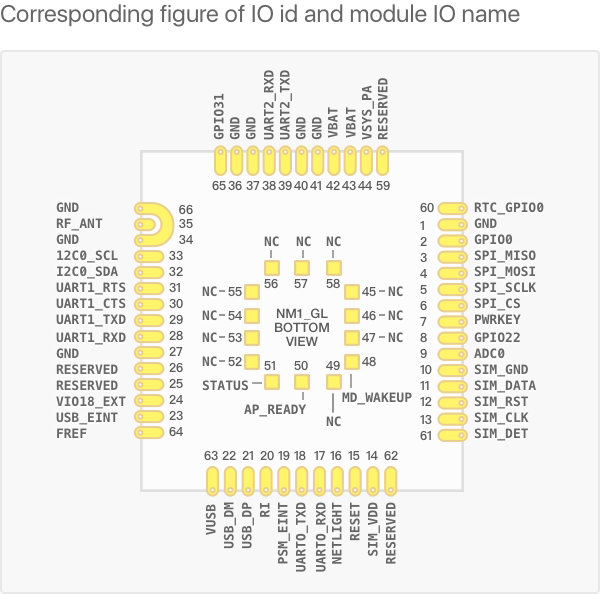
Pin definition
| Pin number | Symbol | I/O type | Functions | Remarks |
|---|---|---|---|---|
| 1 | GND | - | - | - |
| 2 | GPIO0 | I/O | GPIO0 | 1.8V, GPIO0 needs to be pulled down to the low level in the USB download mode,do not pull down before power on, otherwise it will not start |
| 3 | SPI_MISO | I | Master input slave output/GPIO14 | 1.8V, master mode |
| 4 | SPI_MOSI | O | Master output slave input/GPIO13 | 1.8V, master mode |
| 5 | SPI_SCLK | O | Serial clock signal/GPIO15 | 1.8V, master mode |
| 6 | SPI_CS | O | Chip selection signal/GPIO12 | 1.8V, master mode |
| 7 | PWRKEY | I | Pull down PWRKEY to start the module | VIL max=0.3 * VBAT and VIH min=0.7 * VBAT |
| 8 | GPIO22 | I/O | GPIO22 | A common GPIO interface |
| 9 | ADC0 | I | A universal analog-to-digital converter | 0 to 1.4V (by default, the firmware does not support ADC0) |
| 10 | SIM_GND | - | SIM card dedicated ground | - |
| 11 | SIM_DATA | - | SIM card data signal | |
| 12 | SIM_RST | - | SIM card reset signal | VOL max=0.15 * SIM_VDD, VOH min=0.85 * SIM_VDD |
| 13 | SIM_CLK | - | SIM card clock signal | VOL max=0.15 * SIM_VDD, VOH min=0.85 * SIM_VDD |
| 14 | SIM_VDD | - | SIM card power supply | - |
| 15 | RESET | I | Reset module | 3.3V, active low |
| 16 | NETLIGHT | O | Network indication | A common GPIO interface. If you need the network indication function, the pin is recommended. |
| 17 | UART0_RXD | I | A main serial interface, which is used for receiving data | 1.8V Please pay attention to reference level conversion |
| 18 | UART0_TXD | O | A main serial interface, which is used for transmitting data | 1.8V Please pay attention to reference level conversion |
| 19 | PSM_EINT | I | An external interrupt pin, which can wake up the module in PSM mode | 3.3V, active low |
| 20 | RI* | O | Ring output prompt | By default, the pin is at a low level. When receiving a short message or certain URC, RI remains to be a high level for 120ms and then gets to be at a low level. |
| 21 | USB_DP | I/O | USB data positive signal | When using the USB function, PIN 63 needs the voltage of 3.3V |
| 22 | USB_DM | I/O | USB data minus signal | When using the USB function, PIN 63 needs the voltage of 3.3V |
| 23 | USB_EINT | - | USB_EINT | The internal part of the module has been short-circuited, and the external part can be NC |
| 24 | VIO18_EXT | O | 1.8V output power supply (no output in PSM mode) | Vmin=1.53V,Vnorm=1.8V |
| 25,26 | RESERVED | – | RESERVED | – |
| 27 | GND | - | GND | - |
| 28 | UART1_RXD | I | A default universal docking user serial interface, which is used for receiving data | 1.8V Please pay attention to reference level conversion |
| 29 | UART1_TXD | O | A default universal docking user serial interface, which is used for transmitting data | 1.8V Please pay attention to reference level conversion |
| 30 | UART1_CTS | - | Whether to receive data | 1.8V Please pay attention to reference level conversion |
| 31 | UART1_RTS | - | Whether to transmit data | 1.8V Please pay attention to reference level conversion |
| 32 | I2C0_SDA | I/O | I2C0_data/GPIO7 | A default I2C interface |
| 33 | I2C0_SCL | O | I2C0_clock/GPIO6 | A default I2C interface |
| 34 | GND | - | GND | - |
| 35 | RF_ANT | - | RF_antenna | 50Ω characteristic impedance |
| 36, 37 | GND | - | GND | - |
| 38 | UART2_RXD | I | Receive data | By default, it is a log serial interface. 1.8 V Please pay attention to the reference level conversion |
| 39 | UART2_TXD | O | Transmit data | By default, it is a log serial interface. 1.8 V Please pay attention to the reference level conversion |
| 40, 41 | GND | - | GND | - |
| 42,43 | VBAT | I | Input Baseband power supply | V=2.1V~3.63V, Vnorm=3.3V |
| 44 | VSYS_PA | O | Input RF power supply | V=2.1 to 3.63V, Vnorm=3.3V. Internal short circuit with Vbat |
| 45-47 | NC | – | NC | – |
| 48 | MD_WAKEUP* | - | Module wakes MCU | It can be used as general GPIO |
| 49 | NC | – | NC | – |
| 50 | AP_READY* | - | MCU sleep state detection | It can be used as general GPIO |
| 51 | STATUS* | - | Indicates the working status of the module | It can be used as general GPIO |
| 52-59 | NC | – | NC | – |
| 60 | RTC_GPIO0 | - | DCDC ENABLE | Not recommended for external use |
| 61 | SIM_DET* | - | SIM card insertion detection | It can be used as general GPIO |
| 62 | RESERVED | – | RESERVED | – |
| 63 | VUSB | I | Module USB power supply | The voltage of 3.3V |
| 64 | FREF | - | Reference frequency | - |
| 65 | GPIO31 | - | GPIO31 | General GPIO |
| 66 | GND | - | GND | - |
Note: the asterisk (*) indicates that the function is not supported at present.
Electrical parameters
Absolute electrical parameters
| Parameter | Description | Minimum value | Maximum value | Unit |
|---|---|---|---|---|
| Ts | Storage temperature | -40 | 90 | ℃ |
| VCC | Power supply voltage | 2.1 | 3.63 | V |
| Contact discharge | VBAT, GND | -5 | +5 | kV |
| Contact discharge | Antenna interface | -5 | +5 | kV |
| Contact discharge | Other interfaces | -0.5 | +0.5 | kV |
| Air discharge | VBAT, GND | -10 | +10 | kV |
| Air discharge | Antenna interface | -10 | +10 | kV |
| Air discharge | Other interfaces | -1 | +1 | KV |
Normal working conditions
| Parameter | Description | Minimum value | Typical value | Maximum value | Unit |
|---|---|---|---|---|---|
| Ta | Working temperature | -40 | 25 | 85 | ℃ |
| VBAT | Power supply voltage | 2.1 | 3.3 | 3.63 | V |
| VCC | IO voltage | - | 1.8 | - | V |
| VIL | IO low-level intput | -0.3 | - | VCC*0.25 | V |
| VIH | IO high-level input | VCC*0.75 | - | VCC | V |
| VOL | IO low-level output | - | - | VCC*0.1 | V |
| VOH | IO high-level output | VCC*0.8 | - | VCC | V |
| Imax | IO drive current | - | - | 12 | mA |
TX and RX Power consumption
| Working mode | Description | Average value | Peak value (Typical value) | Unit |
|---|---|---|---|---|
| PSM | Deep Sleep | 3 | - | μA |
| Idle | eDRX=81.92S, PTW=40.96S | 287 | - | μA |
| Idle | @DRX=1.28S | 540 | - | μA |
| Idle | @DRX=2.56S | 436 | - | μA |
| Single-tone carrier frequency of 3.75kHz | B1@23 dBm | 205 | 290 | mA |
| Single-tone carrier frequency of 3.75kHz | B2@23 dBm | 195 | 272 | mA |
| Single-tone carrier frequency of 3.75kHz | B3@23 dBm | 185 | 258 | mA |
| Single-tone carrier frequency of 3.75kHz | B4@23 dBm | 185 | 258 | mA |
| Single-tone carrier frequency of 3.75kHz | B5@23 dBm | 199 | 289 | mA |
| Single-tone carrier frequency of 3.75kHz | B8@23 dBm | 201 | 288 | mA |
| Single-tone carrier frequency of 3.75kHz | B20@23 dBm | 199 | 287 | mA |
| Single-tone carrier frequency of 3.75kHz | B28@23 dBm | 221 | 317 | mA |
RF parameters
Basic RF features
| Parameter | Description |
|---|---|
| Working frequency | |
| B1 | Uplink: 1920 to 1980 MHz; Downlink: 2110 to 2170 MHz |
| B2 | Uplink: 1850 to 1910 MHz; Downlink: 1930 to 1990 MHz |
| B3 | Uplink: 1710 to 1785 MHz; Downlink: 1805 to 1880 MHz |
| B4 | Uplink: 1710 to 1755 MHz; Downlink: 2110 to 2155 MHz |
| B5 | Uplink: 824 to 849 MHz; Downlink: 869 to 894 MHz |
| B8 | Uplink: 880 to 915 MHz; Downlink: 925 to 960 MHz |
| B20 | Uplink: 832 to 845 MHz; Downlink: 875 to 890 MHz |
| B28 | Uplink: 703 to 748 MHz; Downlink: 758 to 803 MHz |
| NB-IoT standards | 3GPP 36.521 |
| 6.2.2F | UE maximum output power for category NB2 |
| 6.2.3F | Maximum power reduction (MPR) for category NB2 |
| 6.2.5F | Configured UE transmitted output power for UE category NB2 |
| 6.3.2F | Minimum output power for category NB2 |
| 6.3.3F | Transmit off power for category NB2 |
| 6.3.4 F1 | ON/OFF time mask for category NB2 |
| 6.3.4.F2 | NPRACH time mask for category NB2 |
| 6.3.5F.2 | Power control relative power tolerance for category NB2 |
| 6.3.5F.1 | Power control absolute power tolerance for category NB2 |
| 6.5.1F | Frequency error for category NB2 |
| 6.5.2.1F.1 | Error vector magnitude (EVM) for category NB2 |
| 6.5.2.2F | Carrier leakage for category NB2 |
| 6.5.2.3F | In-band emissions for non-allocated RB for category NB2 |
| 6.6.1F | Occupied bandwidth for category NB2 |
| 6.6.2.1F | Spectrum emission mask for category NB2 |
| 6.6.2.3F | Adjacent channel leakage power ratio for category NB2 |
| 7.3F.1 | Reference sensitivity level without repetitions for category NB2 |
| 7.4F | Maximum input level for category NB2 |
| Data transmission rate | R13: Single-tone: 25.5 kbps (downlink), 16.7 kbps (uplink) Multi-tone: 25.5 kbps (downlink), 62.5kbps (uplink) |
| Data transmission rate | R14: Multi-tone: 102 kbps (downlink) and 157 kbps (uplink) |
| Antenna type | Antenna provided by the third party (external antenna, FPC antenna, etc.) |
TX performance
| Frequency band | Minimum value | Maximum value | Unit |
|---|---|---|---|
| B1 | <-39 | 23 dBm±2 dB | dBm |
| B2 | <-39 | 23 dBm±2 dB | dBm |
| B3 | <-39 | 23 dBm±2 dB | dBm |
| B4 | <-39 | 23 dBm±2 dB | dBm |
| B5 | <-39 | 23 dBm±2 dB | dBm |
| B8 | <-39 | 23 dBm±2 dB | dBm |
| B20 | <-39 | 23 dBm±2 dB | dBm |
| B28 | <-39 | 23 dBm±2 dB | dBm |
RX performance
| Frequency band | Typical value | Unit |
|---|---|---|
| Band 1 | -125 dBm/15 kHz | dBm |
| Band 2 | -125 dBm/15 kHz | dBm |
| Band 3 | -125 dBm/15 kHz | dBm |
| Band 4 | -125 dBm/15 kHz | dBm |
| Band 5 | -125 dBm/15 kHz | dBm |
| Band 8 | -125 dBm/15 kHz | dBm |
| Band 20 | -125 dBm/15 kHz | dBm |
| Band 28 | -125 dBm/15 kHz | dBm |
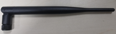
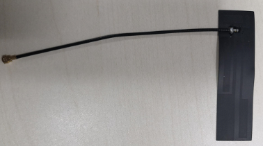
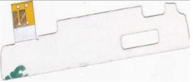
Antenna
Antenna type
The module does not have its onboard PCB antenna, and the third party needs to provide an antenna.
The antenna can be an external rod antenna, a spring antenna, an IPEX-FPC antenna, a PCB board antenna, etc. The antenna forms include monopole antenna, PIFA antenna, IFA antenna, loop antenna, etc.
Antenna interference reduction
To ensure optimal NB-IoT performance, it is recommended that the antenna be at least 10 mm away from other metal parts.
Packaging and production instructions
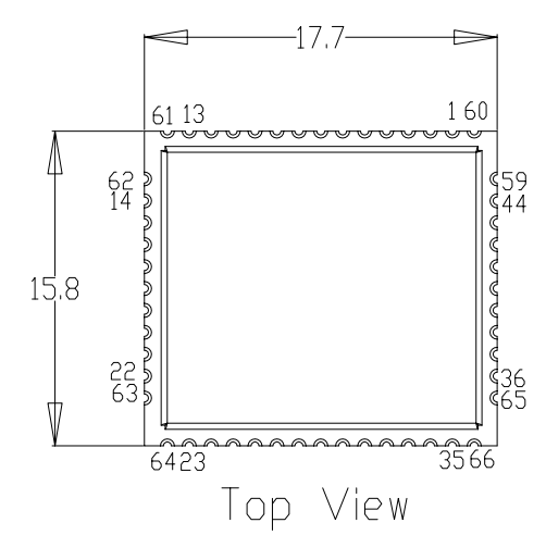
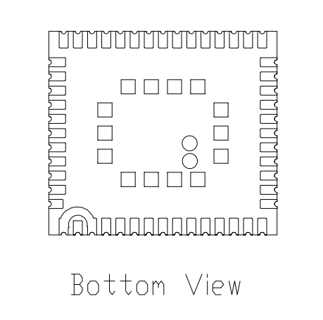
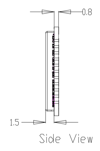
Mechanical dimensions
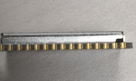
NM1-GL has 66 pins in total. 52 pins are LCC package, and 14 pins are LGA package.
The NM1-GL dimensions are 17.7±0.35mm (L)×15.8±0.35mm (W) ×2.3±0.15mm (H), which are shown as belows:
The PCB thickness tolerance is ±0.1mm.
Top and bottom view
Side view
Schematic diagram of packaging
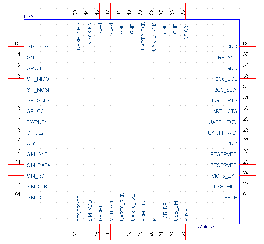
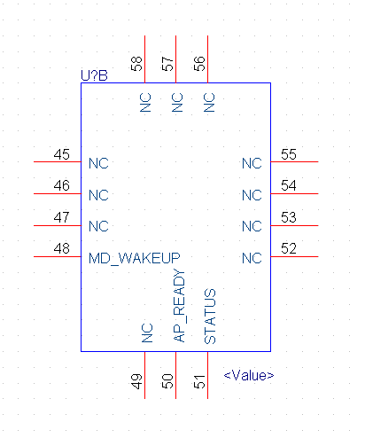
Diagram of PCB packaging-SMT
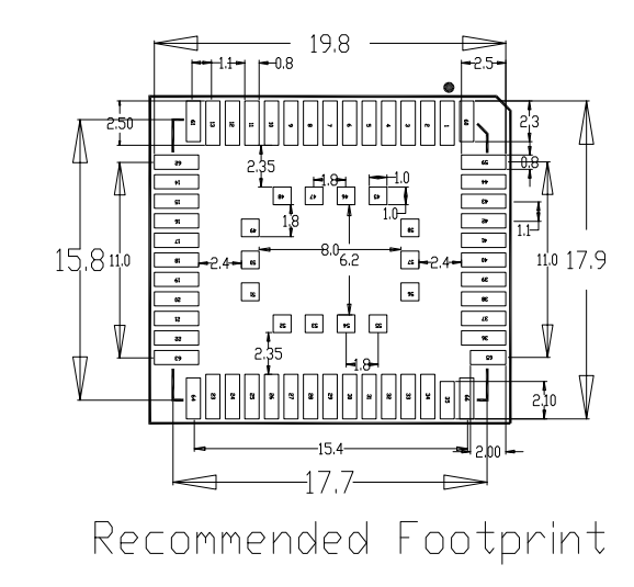
Top/Bottom/Side view of the module
Production instructions
-
The stamp-hole module must be mounted by the SMT machine. After being unpacked, it must be soldered within 24 hours. Otherwise, it must be put into the drying cupboard where the RH is not greater than 10%, or it needs to be packaged under vacuum again and the exposure time needs to be recorded (the total exposure time cannot exceed 168 hours).
- SMT equipment:
- Mounter
- SPI
- Reflow soldering machine
- Oven temperature tester
- Automated optical inspection (AOI) equipment
- Baking equipment:
- Cabinet oven
- Anti-static heat-resistant pallets
- Anti-static heat-resistant gloves
- SMT equipment:
-
Storage conditions for a delivered module are as follows:
- The moisture-proof bag must be placed in an environment where the temperature is below 40°C and the relative humidity is lower than 90%.
- The shelf life of a dry-packaged product is 12 months from the date when the product is packaged and sealed.
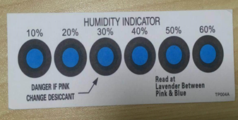
- The package contains a humidity indicator card (HIC).
-
The module needs to be baked in the following cases:
- Vacuum packing bag was found to be damaged before being unpacked.
- There is no humidity indicator card (HIC) in the vacuum packing bag.
- After being unpacked, 10% and above circles on the HIC become pink.
- The total exposure time has been more than 168 hours since unpacking.
- More than 12 months have passed since the sealing date of the bag.
-
Baking settings:
- Temperature: 60°C and ≤ 5%RH for reelizing and 125°C and ≤5%RH for palletizing (please use heat-resistant pallet rather than plastic pallet)
- Time: 48 hours for reelizing and 12 hours for palletizing
- Alarm temperature: 65°C for reelizing and 135°C for palletizing
- Production ready temperature after natural cooling: < 36°C
- The number of drying times: 1
- Re-baking condition: If a module remains unused for 168 hours after being unpacked, it must be baked again.
Important: If this batch of modules is not baked within 168 hours, do not use the wave soldering to solder them. Because these modules are 3-level moisture-sensitive components, they are very likely to get damp when exposed outside. In this case, if they are soldered at high temperatures, it may result in component failure or poor soldering.
-
In the whole production process, take electrostatic discharge (ESD) protective measures.
-
To guarantee the passing rate, it is recommended that you use the SPI and AOI to monitor the quality of solder paste printing and mounting.
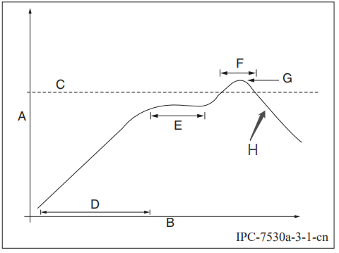
Recommended oven temperature curve
Perform mounting with the SMT based on the following reflow oven temperature curve. The highest temperature is 245°C. The reflow temperature curve is as below:
-
A: Temperature axis
-
B: Time axis
-
C: Liquidus temperature: 217 to 220°C
-
D: Ramp-up slope: 1 to 3°C/s
-
E: Duration of constant temperature: 60 to 120s; the range of constant temperature: 150 to 200°C
-
F: Duration above the liquidus: 50 to 70s
-
G: Peak temperature: 235 to 245°C
-
H: Ramp-down slope: 1 to 4°C/s
Note: The above curve is just an example of the solder paste SAC305. For more details about other solder pastes, please refer to Recommended oven temperature curve in the solder paste specifications.
Storage conditions

MOQ and packaging information
| Product number | MOQ | Shipping packaging method | Number of modules per reel | Number of reels per carton |
|---|---|---|---|---|
| NM1-GL | 5600 | Tape reel | 1400 | 4 |
Is this page helpful?
YesFeedbackIs this page helpful?
YesFeedback


