BDU Module Datasheet
BDU module is a Bluetooth Low Energy (LE) module developed by Tuya Smart. It consists of a highly integrated Bluetooth chip CC2340R5 and a few peripheral circuits. It has built-in Bluetooth protocol stacks and a rich set of library functions.
Overview
The BDU module is built around a 32-bit MCU with 512 KB flash memory and 36 KB SRAM. It has 16 GPIOs. The embedded 2.4 GHz transceiver supports Bluetooth 5.4 low energy.
Features
- Built-in low-power 32-bit MCU that also acts as an application processor
- Clock rate of 48 MHz
- Operating voltage range: 1.71V to 3.8V
- Peripherals: 5 pulse-width modulator (PWM) pins
- Bluetooth LE radio frequency (RF) features
- Bluetooth LE 5.4
- Support data rates 125 Kbit/s, 500 Kbit/s, 1 Mbit/s, and 2 Mbit/s
- Transmitter (TX) power: +8 dBm
- Receiver (RX) sensitivity: -95 dBm@Bluetooth LE 1 Mbit/s
- Embedded hardware Advanced Encryption Standard (AES) encryption
- Onboard PCB antenna with a gain of 1.44 dBi
- Operating temperature range: -40°C to +85°C
Scope of applications
- Smart water detector
- Smart home
- Smart low power sensor
Module interfaces
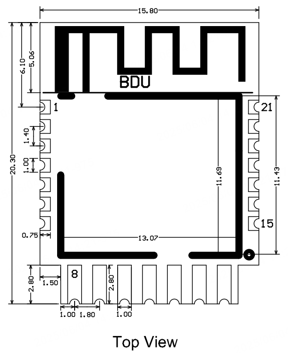
Dimensions and footprint
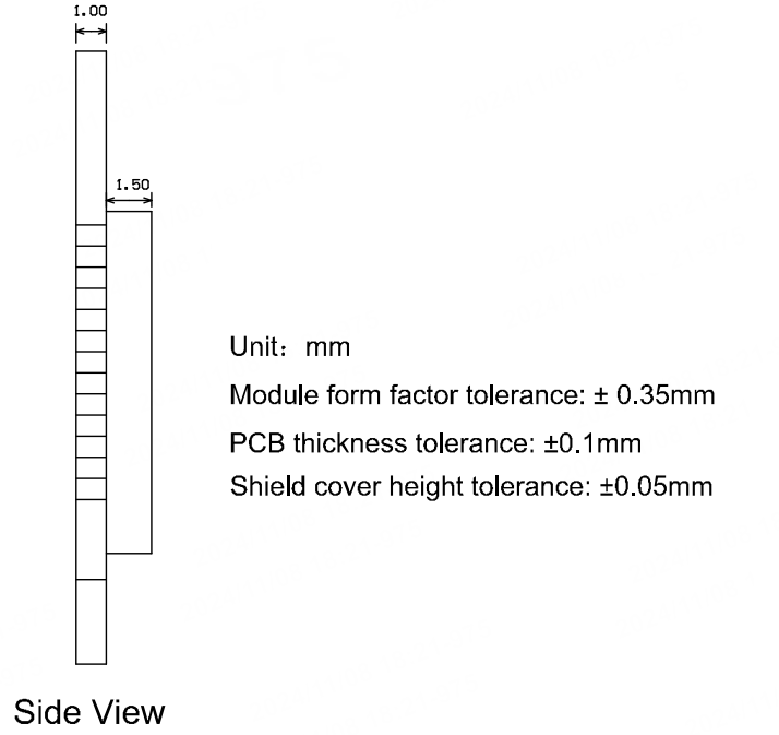
The BDU module has a total of 21 pins in 3 rows. The pin spacing is 1.4±0.1 mm on both sides and 1.8±0.1 mm at the bottom.
The dimensions are 20.3±0.35 mm (L) × 15.8±0.35 mm (W) × 2.5±0.15 mm (H). The PCB thickness is 1.0±0.1 mm. The footprint is shown in the figure:
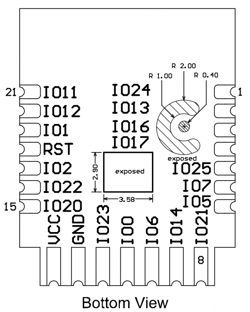
Pin definition
The following table lists the pin definitions.
| No. | Symbol | I/O type | Feature |
|---|---|---|---|
| 1 | IO24 | I/O | GPIO pin, can be reused as SPI_SCLK, corresponding to DIO24 on the IC. |
| 2 | IO13 | I/O | GPIO pin, can be reused as SPI_MOSI, corresponding to DIO13 on the IC. |
| 3 | IO16 | I/O | GPIO pin, corresponding to DIO16 on the IC. |
| 4 | IO17 | I/O | GPIO pin, corresponding to DIO17 on the IC. |
| 5 | IO25 | I/O | GPIO pin, can be reused as ADC, corresponding to DIO25 on the IC. |
| 6 | IO7 | I/O | Before powering on, pull down to enter flashing mode, corresponding to DIO7 on the IC. It is generally not recommended to use it as a GPIO pin. |
| 7 | IO5 | I/O | GPIO pin, corresponding to DIO5 on the IC. |
| 8 | IO21 | I/O | PWM0, corresponding to DIO21 on the IC. |
| 9 | IO14 | I/O | PWM3, corresponding to DIO14 on the IC. |
| 10 | IO6 | I/O | PWM1, corresponding to DIO6 on the IC. |
| 11 | IO0 | I/O | PWM3, corresponding to DIO0 on the IC. |
| 12 | IO23 | I/O | PWM2, corresponding to DIO23 on the IC. |
| 13 | GND | P | The GND pin of the module. |
| 14 | VCC | P | VCC pin of power supply. |
| 15 | IO20 | I/O | Serial TX, corresponding to DIO5 on the IC. |
| 16 | IO22 | I/O | Serial RX, corresponding to DIO20 on the IC. |
| 17 | IO2 | I/O | GPIO pin, can be reused as flow control CTS, corresponding to DIO2 on the IC. |
| 18 | RST | I/O | Reset pin. |
| 19 | IO1 | I/O | GPIO pin, can be reused as flow control RTS, corresponding to DIO1 on the IC. |
| 20 | IO12 | I/O | GPIO pin, can be reused as SPI_MISO, corresponding to DIO12 on the IC. |
| 21 | IO11 | I/O | GPIO pin, can be reused as SPI_CSN, corresponding to DIO11 on the IC. |
Pindicates the power pin,I/Oindicates the input and output pin, andAIindicates the analog input signal.- If you have requirements for the color of PWM output control, please contact Tuya’s business personnel.
Electrical parameters
Absolute electrical parameters
| Parameter | Description | Min value | Max value | Unit |
|---|---|---|---|---|
| Ts | Storage temperature | -40 | 150 | °C |
| VCC | Supply voltage | -0.3 | 4.1 | V |
| Electrostatic discharge voltage (human body model) | TAMB-25°C | - | 1 | kV |
| Electrostatic discharge voltage (machine model) | TAMB-25°C | - | 0.5 | kV |
Operating conditions
| Parameter | Description | Min value | Typical value | Max value | Unit |
|---|---|---|---|---|---|
| Ta | Operating temperature | -40 | - | 85 | °C |
| VCC | Operating voltage | 1.71 | 3.3 | 3.8 | V |
| VIL | I/O low-level input | - | - | 0.2 × VDDS | V |
| VIH | I/O high-level input | 0.8 × VDDS | - | - | V |
Power consumption in working mode
| Symbol | Condition | Max (Typical) value | Unit |
|---|---|---|---|
| Itx | Continuous transmission, with an output power of 8 dBm | 16 | mA |
| Irx | Continuous reception | 6.8 | mA |
| IDC | Average value when connected over Bluetooth mesh | 6.7 | mA |
| IDC | Peak value when connected over Bluetooth mesh | 24.9 | mA |
| Ideepsleep1 | Deep sleep mode (16 KB RAM reserved) | 1.2 | μA |
| Ideepsleep2 | Deep sleep mode (RAM not reserved) | 0.4 | μA |
Radio frequency (RF) parameters
Basic RF features
| Parameter | Description |
|---|---|
| Operating frequency | 2.4 GHz ISM band |
| Wireless standard | Bluetooth LE 5.4 |
| Data transmission rate | 125 Kbit/s, 500 Kbit/s, 1 Mbit/s, and 2 Mbit/s |
| Antenna type | Onboard PCB antenna |
RF output power
| Parameter | Min value | Typical value | Max value | Unit |
|---|---|---|---|---|
| RF average output power | -15 | 8 | 8 | dBm |
| Bandwidth of 20 dB modulation signal (1 Mbit/s) | - | 2500 | - | KHz |
| Bandwidth of 20 dB modulation signal (2 Mbit/s) | - | 1400 | - | KHz |
RF receiver (RX) sensitivity
| Parameter | Min value | Typical value | Max value | Unit |
|---|---|---|---|---|
| RX sensitivity at 125 Kbit/s | - | -101 | - | dBm |
| RX sensitivity at 1 Mbit/s | - | -96 | - | dBm |
| Frequency offset error at 1 Mbit/s | -250 | - | +300 | KHz |
| Frequency offset error at 2 Mbit/s | -300 | - | +200 | KHz |
| Co-channel interference suppression | - | -10 | - | dB |
Antenna information
Antenna type
Onboard PCB antenna with a gain of 1.44 dBi.
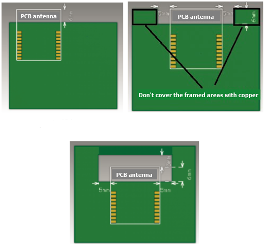
Antenna interference reduction
The distance between the antenna and other metal components should be at least 15 mm to provide the best radio performance. If metal materials wrap the surrounding of the antenna, the wireless signal will be greatly attenuated, thereby deteriorating the RF performance. Allow enough space to support the RF layout when designing your product.
Footprint and production instructions
Mechanical dimensions and backside pad dimensions
Recommended PCB footprint
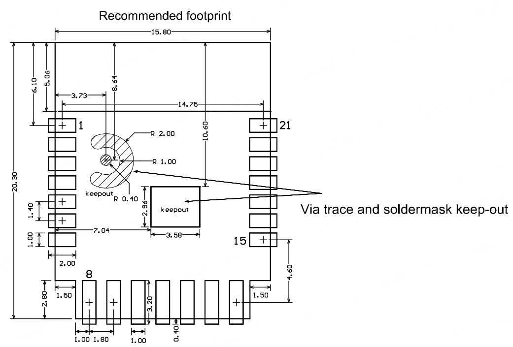
The default tolerance of the external dimensions of the module is ±0.35 mm, and the tolerance of key dimensions is ±0.1 mm. If you have special requirements for key dimensions, specify them in the datasheet after consultations. The area indicated as keep-out in the diagram above does not require tinning and should not have any traces routed through it.
Production instructions
-
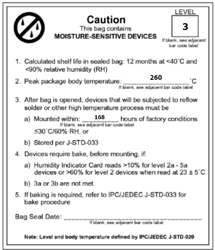
For the modules that can be packaged with the surface-mount technology (SMT) or in in-line form, you can select either of them according to the PCB design solutions of customers. If a PCB is designed to be SMT-packaged, package the module with the SMT. If a PCB is designed to use an in-line package, use wave soldering. Complete soldering within 24 hours after the module is unpacked. Otherwise, place the module in a drying cupboard with a relative humidity level below 10%, or pack the module in vacuum again. Then, record the packing time and duration of exposure. The total exposure time cannot exceed 168 hours.
- Instruments or devices required for the SMT process:
- Surface mount system
- SPI
- Reflow soldering machine
- Thermal profiler
- Automated optical inspection (AOI) equipment
- Instruments or devices required for the wave soldering process:
- Wave soldering device
- Wave soldering fixture
- Constant-temperature soldering iron
- Tin bar, tin wire, and flux
- Thermal profiler
- Instruments or devices required for the baking process:
- Cabinet oven
- Electrostatic discharge (ESD) protection and heat-resistant trays
- ESD protection and heat-resistant gloves
- Instruments or devices required for the SMT process:
-
A delivered module must meet the following storage requirements:
-
The moisture-proof bag must be placed in an environment where the temperature is below 40°C and the relative humidity is lower than 90%.
-
The shelf life of a dry-packaged product is 12 months from the date when the product is packaged and sealed.
-
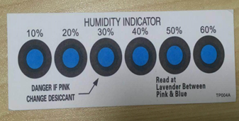
A humidity indicator card (HIC) is put in the sealed package.
-
-
The module needs to be baked in the following cases:
- The vacuum packaging bag is damaged before unpacking.
- After unpacking, no HIC is found in the packaging bag.
- After unpacking, the HIC indicates a humidity level of 10% or higher. In this case, the circle turns pink on the HIC.
- The total exposure time has lasted for over 168 hours since unpacking.
- More than 12 months have passed since the first sealing of the bag.
-
The baking parameter settings are described below:
- Baking temperature: 40°C for reel packaging with relative humidity ≤ 5%. And 125°C for tray packaging with relative humidity ≤ 5% (use the heat-resistant tray, rather than plastic containers).
- Baking time: 168 hours for reel packaging and 12 hours for tray packaging.
- Temperature for triggering an alert: 50°C for reel packaging and 135°C for tray packaging.
- Production can begin after a module has cooled down to below 36°C under natural conditions.
- If a module remains unused for over 168 hours after being baked, it needs to be baked again.
- If a batch of modules is not baked after exposure for more than 168 hours, do not use reflow soldering or wave soldering to solder them. Because these modules are level-3 moisture-sensitive devices, they are very likely to get damp when exposed beyond the allowable time. In this case, if they are soldered at high temperatures, device failure or poor soldering performance might occur.
-
In the whole production process, take electrostatic discharge (ESD) protective measures.
-
To guarantee the pass rate, we recommend that you use the SPI and AOI to monitor the quality of solder paste printing and mounting.
Recommended oven temperature curve
Select a proper soldering technique according to the process. For more information, refer to the recommended oven temperature curve of either reflow soldering or wave soldering. The set temperatures might deviate from the actual temperature measurements. All temperatures shown in this module datasheet are obtained through actual measurements.
Technique 1: SMT process (recommended oven temperature curve of reflow soldering)
Set the oven temperatures according to the following curve.
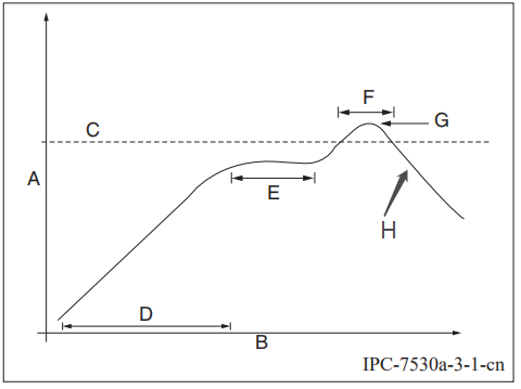
- A: temperature axis
- B: time axis
- C: alloy liquidus temperature from 217°C to 220°C
- D: ramp-up slope from 1°C/s to 3°C/s
- E: keep a constant temperature from 150°C to 200°C for a time period of 60s to 120s
- F: temperature above liquidus temperature for 50s to 70s
- G: peak temperature from 235°C to 245°C
- H: ramp-down slope from 1°C/s to 4°C/s
The curve above is based on solder paste SAC305. For more information about other solder pastes, see the recommended oven temperature curve in the specified solder paste specifications.
Technique 2: Wave soldering process (oven temperature curve of wave soldering)
Set the oven temperatures according to the following temperature curve of wave soldering. The peak temperature is 260°C±5°C.
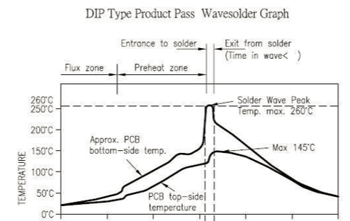
| Suggestions on wave soldering | Suggestions on manual repair soldering | ||
|---|---|---|---|
| Preheat temperature | 80°C to 130°C | Soldering temperature | 360°C ± 20°C |
| Preheat duration | 75s to 100s | Soldering duration | Less than 3s/point |
| Contact duration at the peak | 3s to 5s | N/A | N/A |
| Solder tank temperature | 260°C ± 5°C | N/A | N/A |
| Ramp-up slope | ≤ 2°C/s | N/A | N/A |
| Ramp-down slope | ≤ 6°C/s | N/A | N/A |
Storage conditions
MOQ and packaging information
| Product model | MOQ (pcs) | Shipping packaging | Modules per reel | Reels per carton |
|---|---|---|---|---|
| BDU | 4,400 | Tape and reel | 1,100 | 4 |
Appendix: Statement
FCC Caution: Any changes or modifications not expressly approved by the party responsible for compliance could void the user’s authority to operate this device.
This device complies with Part 15 of the FCC Rules. Operation is subject to the following two conditions: (1) This device may not cause harmful interference, and (2) this device must accept any interference received, including interference that may cause undesired operation.
2.2 List of applicable FCC rules
This module has been tested and found to comply with Part 15C, Section 15.247 requirements for Modular Approval.
2.3 Specific Operational Use Conditions- Antenna Placement Within the Host Platform
The module is tested for standalone mobile RF exposure use condition.
- The antenna must be installed such that 20cm is maintained between the antenna and users,
- The transmitter module may not be co-ocated with any other transmitter or antenna.
In the event that these conditions can‘t be met (for example Certain laptop configurations or co-location with another transmitter), then the FCC authorization is no longer considered valid and the FCC ID can't be used on the final product. In these circumstances, the integrator will be responsible for reevaluating the end product (including the transmitter) and obtaining a separate FCC authorization.
2.4 Limited Module Procedures
Not applicable
2.5 Trace Antenna Designs
Not applicable
2.6 RF Exposure Considerations
This device complies with fcc radiation exposure limits set forth for an uncontrolled environment. This equipment should be installed and operated with minimum distance 20cm between the radiator & your body.
2.7 Antenna Type and Gain
The following antennas have been certified for use with this module. Only antennas of the same type with equal or lower gain may also be used with this module. Other types of antennas and/or higher gain antennas may require the additional authorization for operation.
Antenna Specification list below:
| Antenna Type | Antenna Model No. | Maximum Antenna Gain (dBi) | Frequency Range |
|---|---|---|---|
| PCB Antenna | BDU Antenna | 1.44 dBi | 2402~2480 MHz |
2.8 End Product Labeling:
This transmitter module is authorized only for use in device. The final end product must be labeled in a visible area with the following: "Contains Transmitter Module FCC ID: 2ANDL-BDU" Or "Contains FCC ID: 2ANDL-BDU". The grantee's FCC ID can be used only when all FCC compliance requirements are met. The end product shall bear the following 15.19 statement: This device complies with part 15 of the FCC Rules. Operation is subject to the following two conditions:
(1) This device may not cause harmful interference, and
(2) This device must accept any interference received, including interference that may cause undesired operation.
2.9 Information on Test Modes and Additional Testing Requirements
The module is tested for standalone mobile RF exposure use condition. Any other usage conditions such as co-location with other transmitter(s) or being used in a portable condition will need a separate reassessment through a class Il permissive change application or new certification.
Host manufacturer installed this modular with single modular approval should perform the test of radiated emission and spurious emission according to FCC part 15C, 15.209, 15.207 requirement, only if the test result comply with FCC part 15C 15.209,15.207 requirement, then the host can be sold legally.
2.10 Additional testing, Part 15 Subpart B Disclaimer
This transmitter modular us tested as a subsystem and its certification does not cover the FCC Part 15 Subpart B rules requirement applicable to the final host. The final host will still need to be reassessed for compliance to this portion of rules requirements if applicable.
As long as all conditions above are met, further transmitter test will not be required. However, the OEM integrator is still responsible for testing their end-product for any additional compliance requirements required with this modular installed.
2.11 Manual Information to the End User:
The OEM integrator has to be aware not to provide information to the end user regarding how to install or remove this RF module in the User Manual of the end product which integrates this module. The end user manual shall include all required regulatory information/warning as show in this manual.
The host integrator must follow the integration instructions provided in this document and ensure that the composite-system end product complies with the requirements by a technical assessment or evaluation to the rules and to KDB Publication 996369.
The host integrator installing this module into their product must ensure that the final composite product complies with the requirements by a technical assessment or evaluation to the rules, including the transmitter operation and should refer to guidance in KDB 996369.
OEM/Host Manufacturer Responsibilities:
Manufacturers are ultimately responsible for the compliance of the Host and Module. The final product must be reassessed against all the essential requirements of the FCC rule such as FCC Part 15 Subpart B before it can be placed on the US market. This includes reassessing the transmitter module for compliance with the Radio and EMF essential requirements of the FCC rules. The module must not be incorporated into any other device or system without retesting for compliance as multi-radio and combined equipment.
2.12 How to Mike Changes-Important Note:
In the event that these conditions can‘t be met (for example Certain laptop configurations or co-location with another transmitter), then the FCC authorization is no longer considered valid and the FCC ID can't be used on the final product. In these circumstances, the integrator will be responsible for reevaluating the end product (including the transmitter) and obtaining a separate FCC authorization.
Declaration of Conformity European Notice

Hereby, Hangzhou Tuya Information Technology Co., Ltd declares that this module product is in compliance with essential requirements and other relevant provisions of Directive 2014/53/EU,2011/65/EU. A copy of the Declaration of conformity can be found at https://www.tuya.com.

This product must not be disposed of as normal household waste, in accordance with the EU directive for waste electrical and electronic equipment (WEEE-2012/19/EU). Instead, it should be disposed of by returning it to the point of sale, or to a municipal recycling collection point.
The device could be used with a separation distance of 20cm to the human body.
ISED Statement
This device complies with Innovation, Science and Economic Development Canada's licence-exempt RSSs. Operation is subject to the following two conditions:
(1) This device may not cause interference.
(2) This device must accept any interference, including interference that may cause undesired operation of the device.
Le présent appareil est conforme aux CNR d’Innovation, Sciences et Développement économique Canada applicables aux appareils radio exempts de licence. L’exploitation est autorisée aux deux conditions suivantes:
(1) l’appareil ne doit pas produire de brouillage.
(2) l’utilisateur de l’appareil doit accepter tout brouillage radioélectrique sub i, même si le brouillage est susceptible d’en compromettre le fonctionnement.
Radiation Exposure Statement
This equipment complies with IC radiation exposure limits set forth for an uncontrolled environment. This equipment should be installed and operated with minimum distance 20 cm between the radiator & your body.
Déclaration d’exposition aux radiations:
Cet équipement est conforme aux limites d’exposition aux rayonnements ISED établies pour un environnement non contrôlé. Cet équipement doit être installé et utilisé avec un minimum de 20 cm de distance entre la source de rayonnement et votre corps.
L’appareil peut interrompre automatiquement la transmission en cas d’absence d’informations à transmettre ou de panne opé rationnelle. Notez que ceci n’est pas destiné à interdire la transmission d’informations de contrôle ou de signalisation ou l’utilisation de codes répétitifs lorsque cela est requis par la technologie.
This device is intended only for OEM integrators under the following conditions:
(1) The antenna must be installed such that 20 cm is maintained between the antenna and users.
(2) The transmitter module may not be co-located with any other transmitter or antenna. As long as 2 conditions above are met, further transmitter test will not be required.
However, the OEM integrator is still responsible for testing their end-product for any additional compliance requirements required with this module installed.
Cet appareil est conçu uniquement pour les intégrateurs OEM dans les conditions
suivantes: (Pour utilisation de dispositif module)
(1) L’antenne doit être installée de telle sorte qu’une distance de 20 cm est respectée entre l’antenne et les utilisateurs.
(2) Le module émetteur peut ne pas être coïmplanté avec un autre é metteur ou antenne.
Tant que les 2 conditions ci-dessus sont remplies, des essais supplé mentaires sur l’émetteur neseront pas nécessaires. Toutefois, l’intégrateur OEM est toujours responsable des essais sur son produit final pour toutes exigences de conformité supplémentaires requis pour ce module installé.
IMPORTANT NOTE:
In the event that these conditions can not be met (for example certain laptop configurations or colocation with another transmitter), then the Canada authorization is no longer considered valid and the IC ID can not be used on the final product. In these circumstances, the OEM integrator will be responsible for re-evaluating the end product (including the transmitter) and obtaining a separate Canada authorization.
NOTE IMPORTANTE:
Dans le cas où ces conditions ne peuvent être satisfaites (par exemple pour certaines configurations d’ordinateur mobile ou de certaines co-localisation avec un autre émetteur), l’autorisation du Canada n’est plus considéré comme valide et l’ID IC ne peut pas être utilisé sur le produit final. Dans ces circonstances, l’intégrateur OEM sera chargé de réévaluer le produit final (y compris l’émetteur) et l’obtention d’une autorisation distincte au Canada.
End Product Labeling
This transmitter module is authorized only for use in device where the antenna may be installed such that 20 cm may be maintained between the antenna and users. The final end product must be labeled in a visible area with the following: "Contains IC:23243-BDU" .
Plaque signalétique du produit final
Ce module émetteur est autorisé uniquement pour une utilisation dans un dispositif où l’antenne peut être installée de telle sorte qu’une distance de 20cm peut être maintenue entre l’antenne et les utilisateurs. Le produit final doit être étiqueté dans un endroit visible avec l’inscription suivante: "Contient des IC:23243-BDU".
Manual Information To the End User
The OEM integrator has to be aware not to provide information to the end user regarding how to install or remove this RF module in the user’s manual of the end product which integrates this module.
The end user manual shall include all required regulatory information/warning as show in this manual.
Manuel d’information à l’utilisateur final
L’intégrateur OEM doit être conscient de ne pas fournir des informations à l’utilisateur final quant à la façon d’installer ou de supprimer ce module RF dans le manuel de l’utilisateur du produit final qui intègre ce module.
Le manuel de l’utilisateur final doit inclure toutes les informations réglementaires requises et avertissements comme indiqué dans ce manuel.
Is this page helpful?
YesFeedbackIs this page helpful?
YesFeedback


