S130N-ISI Module Datasheet
Overview
The S130N-ISI module is a fully integrated power line communication (PLC) module based on Unicomsemi VC6330 chip design. It incorporates a 32-bit ARM Cortex-M4 MCU, 32-bit DSP, embedded flash memory, 1 MB SRAM, and abundant communication interfaces.
The module adopts an LCC package design, featuring ultra-compact dimensions and a highly integrated structure. With built-in line drivers, it delivers low power consumption and excellent noise immunity. This solution is ideally suited for various PLC real-time communication applications, including smart street lighting, smart home systems, central air conditioning, and ubiquitous electrical IoT edge devices.
Description
| Parameter | Description |
|---|---|
| Module model | S130N-ISI |
| Main IC | VC6330 |
| Dimensions | L × W × H: 20.6 (±0.25) mm × 12.6 (±0.2) mm × 2.5 (±0.25) mm |
| Interfaces | UART, PWM, EPWM, GPIO, ADC, SPI, and I2C |
| Communication methods | The power line carrier communication supports both AC power grids (220V/110V) and low-voltage DC power grids. |
| Operating temperature | FGS130NISI-YWX-K0: -40°C to +85°C FGS130NISI-YWX-K1: -40°C to +105°C |
| Storage temperature | -40°C to +125°C |
| Power input | 3.3V ± 100mV |
Certain models support operation at 105°C. For more information, refer to the Ordering information.
Features
-
CPU and storage:
- 32-bit ARM Cortex-M4 MCU with 32-bit DSP
- 2 MB on-chip flash memory
- 1 MB on-chip SRAM
-
PLC PHY
- Support 0 to 12 MHz bandwidth (SGCC standard) with multiple available sub-bands
- Comply with China SGCC Q/GDW 11612 protocol
- Comply with IEEE 1901.1 protocol
- Support modulation schemes: BPSK, QPSK, and 16QAM
-
Peripheral interfaces
- UART interface, GPIO interface, PWM/EPWM output, ADC input, SPI interface, and I2C interface
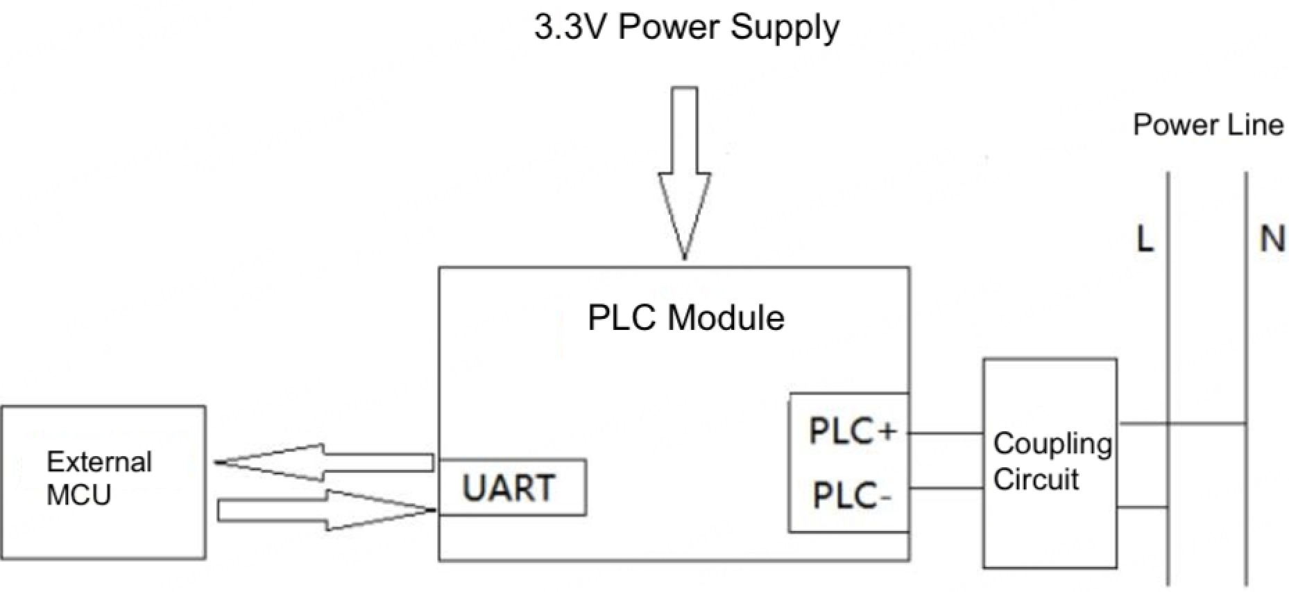
Block diagram
The following figure shows a typical application circuit:
Pin definition
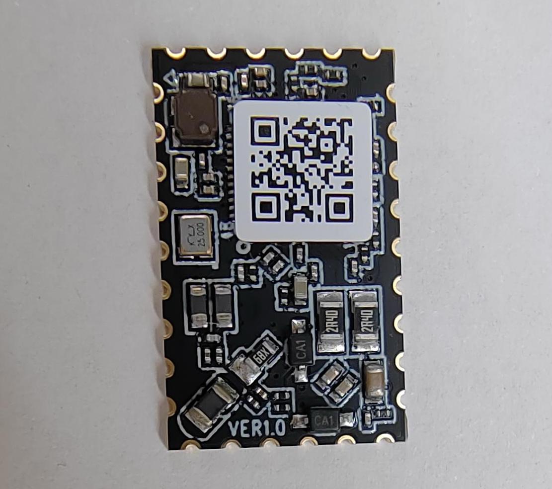
Module appearance
Pinout
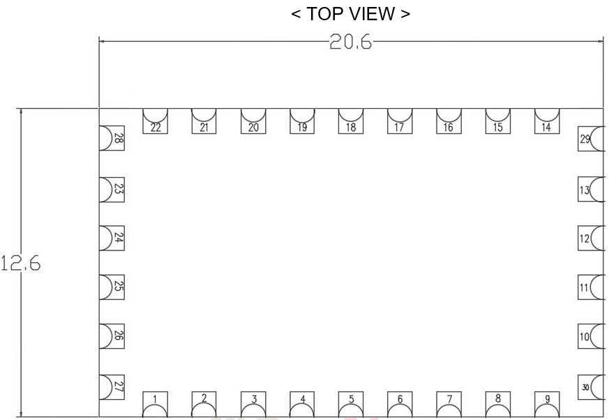
Pin features
| Pin No. | Definition | Description |
|---|---|---|
| 1 | IOB10/I2C_SCL/SPI_CLK | Defaults to GPIOB10 for general-purpose input/output.
|
| 2 | IOB12/SPI_MOSI | Defaults to GPIOB12 for general-purpose input/output. Alternative signal 1: SPI master output/slave input. When in use, connect a 56Ω damping resistor in series. |
| 3 | IOB11/I2C_SDA/SPI_MISO | Defaults to GPIOB11 for general-purpose input/output.
|
| 4 | IOA0/ADC_VIN6 | Defaults to GPIOA0 for general-purpose input/output. Alternative signal 1: ADC_VIN6, ADC input, sampling voltage range 0 to 3.3V, sampling accuracy 12 bits. When used as a GPIO pin, connect a 56Ω damping resistor in series. |
| 5 | IOB9/SPI_CS | Defaults to GPIOB9 for general-purpose input/output. Alternative signal 1: SPI chip select. When in use, connect a 56Ω damping resistor in series. |
| 6 | When in use, connect a 56Ω damping resistor in series. | Defaults to GPIOB13 for general-purpose input/output.
|
| 7 | IOE2/EPWM4_A | Defaults to GPIOE2 for general-purpose input/output. Alternative signal 1: EPWM4 Channel A. When in use, connect a 56Ω damping resistor in series. This pin must not be pulled up, otherwise, the module will fail to start properly. |
| 8 | IOA6_EPWM0_A | Defaults to GPIOA6 for general-purpose input/output. Alternative signal 1: EPWM0 Channel A. When in use, connect a 56Ω damping resistor in series. |
| 9 | IOA1/ADC_VIN5 | Defaults to GPIOA1 for general-purpose input/output. Alternative signal 1: ADC_VIN5, ADC input, sampling voltage range 0 to 3.3V, sampling accuracy 12 bits. When used as a GPIO pin, connect a 56Ω damping resistor in series. |
| 10 | PLC- | Protective and coupling circuits must be implemented to isolate AC power lines. Standard protection rating is ±4kV in differential mode and common mode. |
| 11 | PLC+ | Protective and coupling circuits must be implemented to isolate AC power lines. Standard protection rating is ±4kV in differential mode and common mode. |
| 12 | GND | Ground. |
| 13 | 3V3 | 3.3V power input pin. |
| 14 | RESETN | Reset pin. Active low. |
| 15 | IOA5 | Defaults to GPIOA5 for general-purpose input/output. When in use, connect a 56Ω damping resistor in series. |
| 16 | NC | It is not connected by default, with limited availability when I/O resources are insufficient. For specific applications, contact the technical support. |
| 17 | IOB1/U5_RX/EPWM2_A | Defaults to UART5_RX to receive serial data and communicate with an external MCU. Use UART5 when an external RS-485 transceiver is required. The module has an internal 10 kΩ pull-up resistor.
|
| 18 | IOB7/U5_TX/EPWM2_B | Defaults to UART5_TX to transmit serial data and communicate with an external MCU. Use UART5 when an external RS-485 transceiver is required. Alternative signal 1: GPIOB7 for general-purpose input/output. Alternative signal 2: EPWM2 Channel B. |
| 19 | ADC_VIN1 | ADC input, sampling voltage range 0 to 3.3V, and sampling accuracy 12 bits. It cannot be used as a GPIO pin. When in use, connect a 56Ω damping resistor in series. |
| 20 | IOC14/EPWM3_B | Defaults to GPIOC14 for general-purpose input/output. Alternative signal 1: EPWM3 Channel B. When in use, connect a 56Ω damping resistor in series. |
| 21 | IOB15/EPWM5_B | Defaults to GPIOB15 for general-purpose input/output. Alternative signal 1: EPWM5 Channel B. When in use, connect a 56Ω damping resistor in series. |
| 22 | IOB6/PWM1/EPWM1_B | Defaults to GPIOB6 for general-purpose input/output.
|
| 23 | IOC13/EPWM3_A | Defaults to GPIOC13 for general-purpose input/output. Alternative signal 1: EPWM3 Channel A. When in use, connect a 56Ω damping resistor in series. |
| 24 | UART0_RXD | Defaults to UART0_RX for firmware flashing and log printing. The module has an internal 10 kΩ pull-up resistor. |
| 25 | UART0_TXD | Defaults to UART0_TX for firmware flashing and log printing. |
| 26 | IOA7/EPWM0_B | Defaults to GPIOA7 for general-purpose input/output. Alternative signal 1: EPWM0 Channel B. When in use, connect a 56Ω damping resistor in series. |
| 27 | IOA8 | Defaults to GPIOA8 for general-purpose input/output. When in use, connect a 56Ω damping resistor in series. |
| 28 | GND | Ground. |
| 29 | NC | Leave it floating. |
| 30 | GND | Ground. |
Hardware design
Input power requirements
| Input voltage | Minimum | Typical | Maximum | Unit |
|---|---|---|---|---|
| 3V3 | 3.0 | 3.3 | 3.6 | V |
- The maximum value in the table represents the module’s maximum tolerance limit. Exceeding this value might damage the module.
- Put at least one 10 μF ground storage capacitor and one 0.1 μF decoupling capacitor near the module’s 3.3V pin. This way, reduce the power supply ripple voltage, and keep peak-to-peak ripple within 100 mV.
- Provide an independent 3.3V power supply for the module whenever possible. When sharing a 3.3V power supply with other modules on the motherboard, please use 600R/100MHz magnetic beads with a current resistance of 1A or above for isolation.
- The 3.3V power supply should ensure a current of at least 300 mA.
- Ensure proper ground return path design in PCB layout.
Suggestions on I/O design
- For interfaces such as GPIO, PWM, EPWM, and ADC, connect a 56Ω damping resistor in series and place it close to the module. For I/O pull-up and pull-down requirements, refer to the pin definition. If it is unused, leave it floating.
- EPWM1_A and EPWM1_B form a complementary ePWM pair with synchronized frequency. The same applies to EPWM2_A and EPWM2_B, EPWM3_A and EPWM3_B, as well as EPWM5_A and EPWM5_B. When different EPWM frequencies are required, only one signal (either A or B) from each complementary pair can be used.
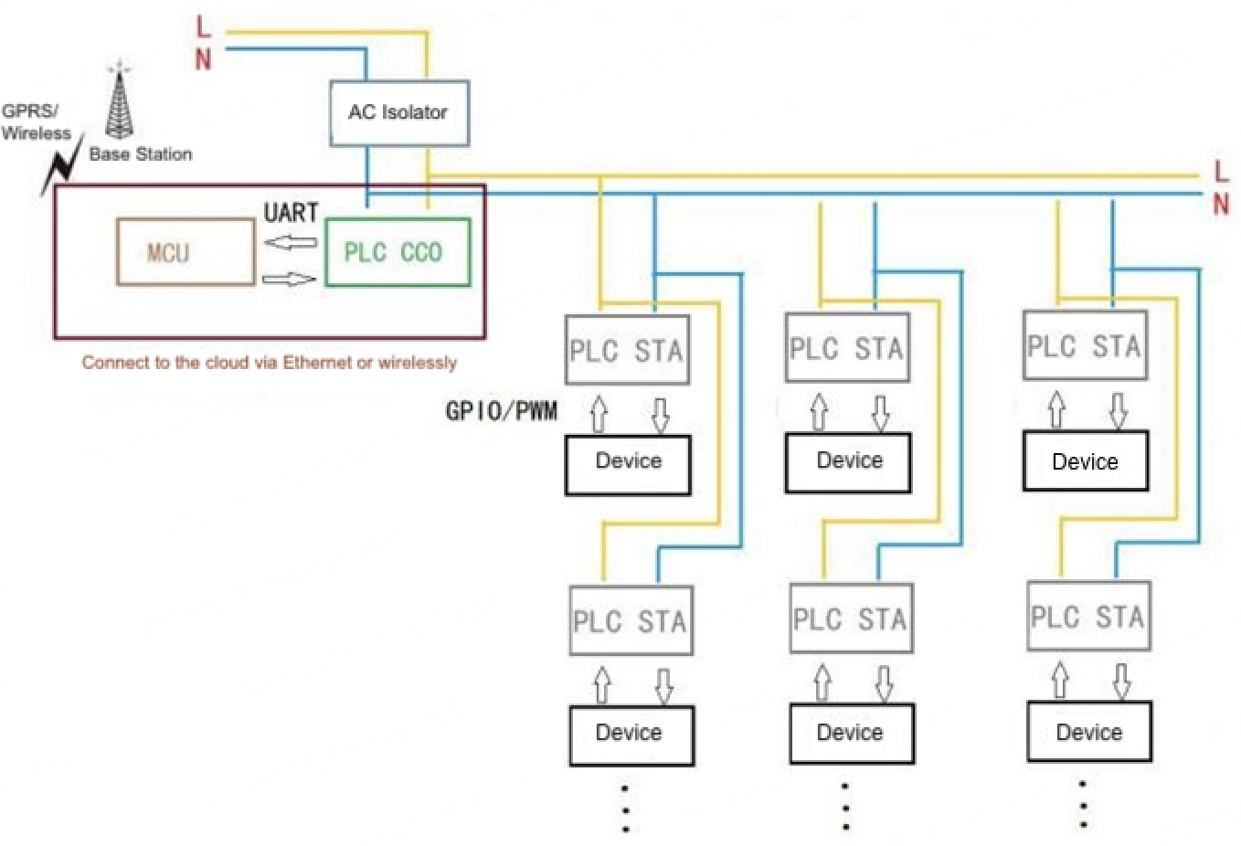
Typical networking diagram of CCO and STA
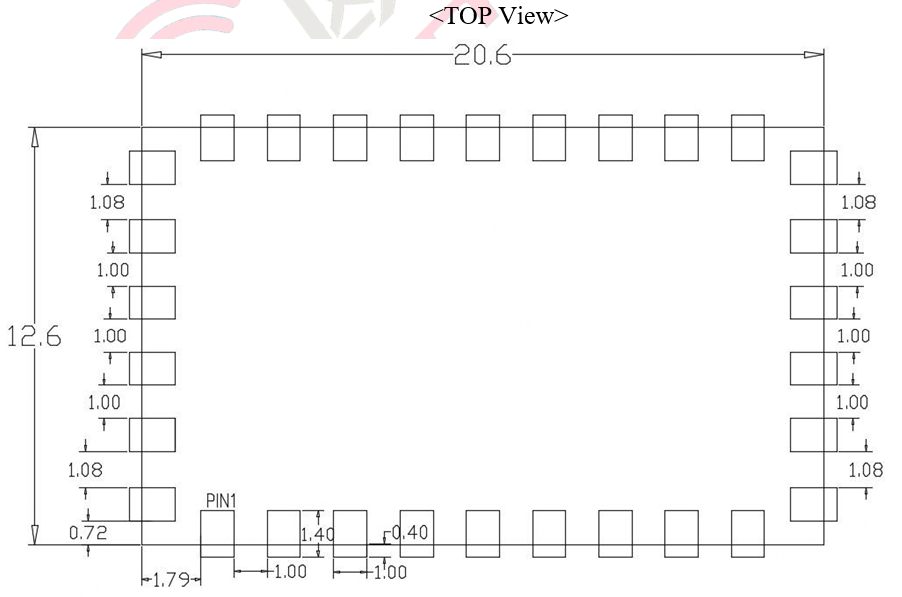
Reference dimensions
Package dimensions
Unit: mm.
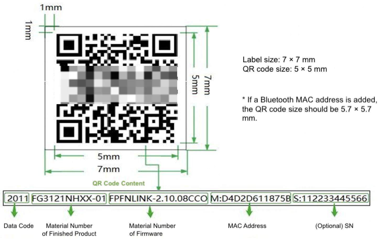
Module label
The shipped module comes with a QR code label containing the following information:
Critical materials
| Material | Specification | Manufacturer |
|---|---|---|
| Main IC | VC6330, 6 × 6 mm, 48L-QFN | Unicomsemi |
| PCB | Matte black, FR4, 4-layer through-hole, TG150, 20.6 × 12.6 × 1.2 mm | Xiangyu, Zhongluo, and Sunlord |
| Crystal oscillator | 2016, 25 MHz, 10 pF ±10 ppm | Jingweite, Dongjing, TKD, Faith Long, and UTECH |
Ordering information
| Part No. | Description |
|---|---|
| FGS130NISI-YWX-K0 | VC6330, PLC module, UART, 30-pin LCC package, 20.6 × 12.6 mm, FCYWXD01, STA, -40 to 85°C |
| FGS130NISI-YWX-K1 | VC6330, PLC module, UART, 30-pin LCC package, 20.6 × 12.6 mm, FCYWXD01, STA, -40 to 105°C |
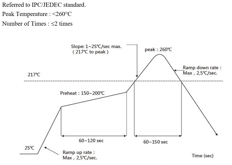
Recommended oven temperature curve
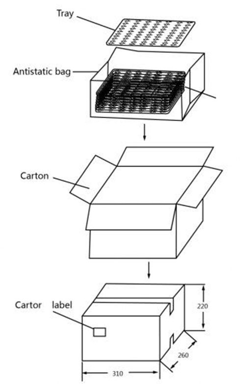
Packaging
Blister packaging
Moisture sensitivity
According to IPC/JEDEC J-STD-020 standards, the module is classified as a Moisture Sensitivity Level 3 (MSL 3) device. Please observe all relevant handling requirements and exercise caution during use.
Additionally, you must pay attention to the following points:
- Shelf life in sealed bag: 12 months at <40°C and <90% relative humidity (RH).
- Production environment conditions: ≤30°C/60% RH as per IPC/JEDEC J-STD-033A Section 5. Baking is required if conditions are unmet.
- Maximum exposure time: <168 hours between sealed bag opening and reflow process. Baking is required if conditions are unmet.
- Compliance: Adhere to IPC/JEDEC J-STD-033A Section 5.2.
- Humidity indicator: Baking is required if the humidity indicator in the bag shows ≥10% RH.
Is this page helpful?
YesFeedbackIs this page helpful?
YesFeedback


