ZTx Series Modules
This topic describes information about implementing serial communication between ZTx series modules and MCUs.
Overview
ZTx series is the Zigbee module developed by Tuya.
This topic applies to the following Zigbee models.
| Module model | Input voltage (TYP) | Average current in continuous TX (250 kbps/+10 dBm) | Average current in continuous RX (250 kbps) | Average current in deep sleep mode |
|---|---|---|---|---|
| ZT3L | 3.3V | 9.15 mA | 7.35 mA | 2.8 μA |
| ZTU-IPEX | 3.3V | 8.9 mA | 6.9 mA | 2.8 μA |
| ZTU | 3.3V | 8.9 mA | 6.9 mA | 2.8 μA |
| ZT5 | 3.3V | 9.1 mA | 6.6 mA | 2.8 μA |
| ZT2S | 3.3V | 9.25 mA | 7.35 mA | 2.8 μA |
| ZTLC5 | 3.3V | 8.66 mA | 6.54 mA | 2.8 μA |
| ZTC | 3.3V | 8.66 mA | 6.54 mA | 2.8 μA |
For more information, see the module datasheet.
- ZT3L Datasheet
- ZTU-IPEX Datasheet
- ZTU Datasheet
- ZT5 Datasheet
- ZT2S Datasheet
- ZTLC5 Datasheet
- ZTC Datasheet
Serial communication protocol
See serial communication protocol for Zigbee protocol.
Serial communication between a module and an MCU
-
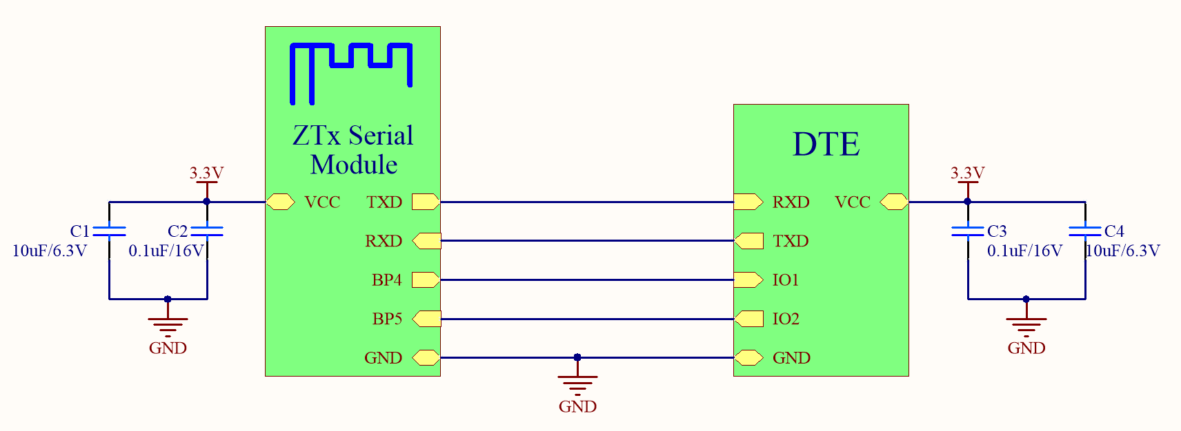
Connection between a module and a 3.3V MCU
-
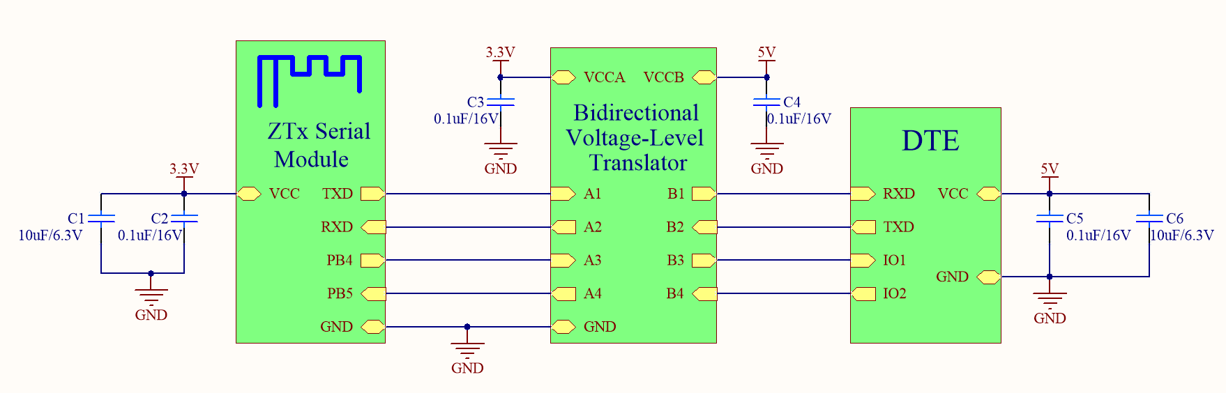
Connection between a module and a 5V MCU
In the following circuit diagram, voltage level translation can be implemented with a bidirectional voltage-level translator, a MOS transistor, or a triode.
Things to note
For low-power devices with sleep mode, two reserved GPIOs (PB4 and PB5) are used for a handshake to make a connection between the MCU and the module. PB4 is used for the Zigbee module to wake up the MCU. PB5 is used for the MCU to wake up the Zigbee module. These two GPIOs default to a high level and need to be pulled low for at least 10 ms to be active.
For battery-powered devices with sleep mode, a handshake is required each time before a party sends a command.
For mains-powered devices without sleep mode, the serial port keeps listening for any connection attempts, so the PB4 and PB5 connection is not necessary.
Level translator reference
-
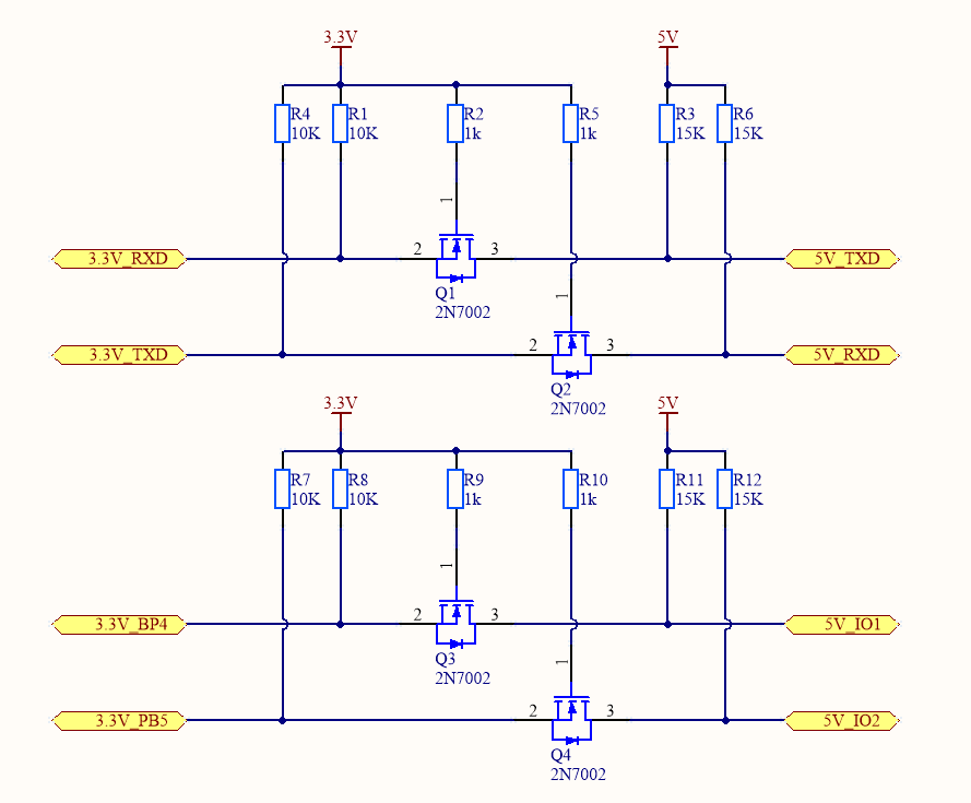
N-channel MOSFET level translator
In the following circuit diagram, an N-channel MOSFET and a built-in body diode are used to implement two-way communication.
-
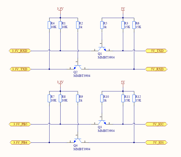
NPN triode level translator
In the following circuit diagram, an NPN triode is used to implement one-way communication.
Design specification
Serial port pin
The following table lists the specification and pin information of ZTx modules for serial communication with an MCU.
| Module model | Peak current in RX (250 kbps/+10 dBm) | TX pin No. | TX silk screen | RX pin No. | RX silk screen | PB4 pin No. | PB4 silk screen | PB5 pin No. | PB5 silk screen |
|---|---|---|---|---|---|---|---|---|---|
| ZT3L | 38.78 mA | 16 | TXD | 15 | RXD | 13 | B4 | 14 | B5 |
| ZTU-IPEX | 38.78 mA | 15 | B1 | 16 | B7 | 11 | B4 | 12 | B5 |
| ZTU | 38.78 mA | 15 | B1 | 16 | B7 | 11 | B4 | 12 | B5 |
| ZT5 | 44 mA | 3 | C2 | 4 | C3 | 1 | B4 | 00 | B5 |
| ZT2S | 38.78 mA | 7 | TX | 5 | RX | 9 | B4 | 11 | B5 |
| ZTLC5 | 38.78 mA | 7 | TX | 5 | RX | - | - | - | - |
| ZTC | 38.7 mA | 3 | TX | 2 | RX | 7 | B4 | 8 | B5 |
The ZTLC5 module does not support serial communication applications applied to low power devices with sleep mode.
Power supply
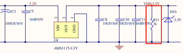
- The supply current for 3.3V modules must be greater than the maximum input current. The total capacity of the external filter capacitor should be greater than 10 μF.
- Place the filter capacitors C1 and C2 near the power pin of the module.
- Given the serial connection between the module and the MCU, if you only shut down the module, the current from the MCU might flow into the power management system of the module, which causes the module to be stuck.
Pins of the module
- The reset pin or enable pin of the module is a hardware reset pin. The module has internal weak pull-up resistors configured. If the pin is not used, it can float. If a module has been paired, this pin cannot be used to clear pairing information.
- The SWS pin of the module is used for firmware flashing. It is not recommended to use it as GPIO. You can leave it floating or add a pull-up resistor.
- Other unused pins can float.
- For more information about pin configuration, see module datasheet.
Power-on sequence of the module
-
Every time a module is powered on, its power pin must be started with 0V.
-
If the voltage of the power pin does not drop to zero after the last power-off, the module will be stuck when it is powered on again.
-
If a capacitor of large capacity connected in the power circuit leads to a slow discharge after power-off, you can connect a 1K dummy load on the 3.3V output to speed up discharge.
Antenna clearance
-
Do not use metal shells or plastic shells with metallic paint or coating in the direction of the antenna radiation. Do not use metal objects such as screws and rivets near the antenna, which might affect the antenna efficiency.
-
Try to increase the distance from the top shell to the antenna to minimize the impact on antenna performance.
-
Try to increase the distance from the upper and bottom shells to the antenna to minimize the impact on antenna performance.
-
Keep the module away from speakers, power switches, cameras, HDMI, USB, and other high-speed signals to avoid interference.
-
Avoid metal shielding near the antenna. If co-channel interference occurs, you must evaluate the impact on the antenna performance and ensure isolation from interference.
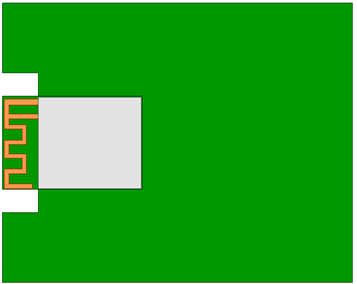
Placement
-
Horizontal placement
We recommend that you place the module at the edge of the backplane with the antenna facing outward, and flush the module’s GND terminal with the backplane’s GND terminal. Both terminals are fully connected.
-
Embedded placement
Embed the module into the backplane through a slot that is flushed with or deeper than the module’s GND terminal. The side of the slot must be 15 mm or farther from the module’s board edge.
A wider slot can achieve better performance that is still weaker than that of horizontal placement.
-
Vertical placement
Insert the module vertically into the backplane slot with the antenna facing upward. The module’s GND terminal and the backplane’s GND terminal must be fully connected. We recommend that you keep a clearance distance of 15 mm or more around the antenna.
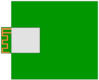
If the RF antenna of the module is traced along the ANT pin and backplane (the PCB board on which the module is mounted) to connect to the antenna, the RF trace (ANT pin is broken out) on the backplane should be surrounded by grounding copper and designed to provide 50Ω impedance matching. The bottom layer under the RF trace should not be traced to ensure a complete ground plane. If you do not use the companion antenna of the module, you can reserve the π network for antenna matching.
Is this page helpful?
YesFeedbackIs this page helpful?
YesFeedback


