ZTLC5 Module Datasheet
ZTLC5 is a Zigbee module that Tuya has developed. It consists of a highly integrated RF chip (Z2) and a few peripherals. ZTLC5 is embedded with a low-power 32-bit CPU, 1024-KB flash memory, 64-KB RAM, and rich peripheral resources.
Overview
Based on ZTLC5, you can develop embedded Zigbee products as required.
Features
- Embedded with low-power 32-bit CPU processor
- The clock rate: 48 MHz
- Wide operating voltage: 1.8 to 3.6 V
- Peripherals: 3 GPIOs, and 1 UART
- Zigbee connectivity
- Support 802.15.4 MAC/PHY
- Working channels 11 to 26 @2.400 to 2.483 GHz, air interface rate: 250 Kbps
- Up to +10dBm output power and dynamic output power > 35 dB
- Monopole antenna with a gain of 1.8 dBi
- Operating temperature: -40℃ to 105℃
- Support hardware encryption and AES 128
Applications
- Intelligent building
- Smart household and home appliances
- Smart socket and light
- Industrial wireless control
- Baby monitor
- Intelligent bus
Module interfaces
Dimensions and package
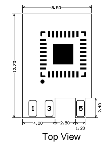
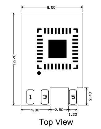
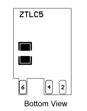
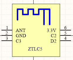
ZTLC5 has 6 pins at the front and back sides for plug-in assembly.
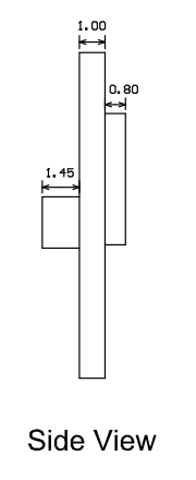
The ZTLC5 dimensions are 8.50±0.35 mm (W)×12.7±0.35 mm (L) ×3.07±0.15 mm (H).
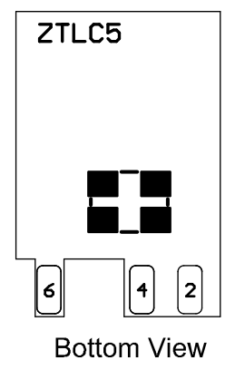
Pin definition
| Pin number | Symbol | I/O type | Function |
|---|---|---|---|
| 1 | ANT | I/O | Antenna pin, external monopole antenna |
| 2 | GND | P | Power supply reference ground |
| 3 | C3 | I/O | Support hardware PWM and correspond to C3 (Pin 23) on the internal IC |
| 4 | D2 | I/O | Support hardware PWM and correspond to D2 (Pin 31) on the internal IC |
| 5 | C2 | I/O | Support hardware PWM and correspond to C2 (Pin 22) on the internal IC |
| 6 | 3V3 | P | Power supply pin of the module (The typical power supply voltage: 3.3V |
| R | RXD | I/O | Uart_RXD, which corresponds to B7 (Pin 17) on the internal IC |
| T | TXD | I/O | Uart_TXD, which corresponds to B1 (Pin 6) of the IC |
| S | SWS | I/O | Burning pin, which corresponds to SWS (Pin 5) on the internal IC |
Note: P indicates a power supply pin and I/O indicates an input/output pin. R, T, and S are the test points
Electrical parameters
Absolute electrical parameters
| Parameter | Description | Minimum value | Maximum value | Unit |
|---|---|---|---|---|
| Ta | Operating temperature | -40 | 105 | ℃ |
| VBAT | Power supply voltage | 1.8 | 3.6 | V |
| ESD voltage (human body model) | TAMB-25℃ | - | 2 | KV |
| ESD voltage (machine model) | TAMB-25℃ | - | 0.5 | KV |
Normal working conditions
| Parameter | Description | Minimum Value | Typical Value | Maximum Value | Unit |
|---|---|---|---|---|---|
| Ta | Operating temperature | -40 | - | 105 | ℃ |
| VCC | Operating voltage | 1.8 | 3.3 | 3.6 | V |
| VIL | I/O low level input | - | - | VDD*0.3 | V |
| VIH | I/O high level input | VDD*0.7 | - | - | V |
| VOL | I/O low level output | - | - | VDD*0.2 | V |
| VOH | I/O high level output | VDD*0.8 | - | - | V |
TX and RX power consumption
| Working status | Mode | Rate | Transmit power/receive | Average value | Peak value (Typical value) | Unit |
|---|---|---|---|---|---|---|
| Transmit | - | 250 Kbps | +0 dBm | 3.85 | 23 | mA |
| Transmit | - | 250 Kbps | +10 dBm | 8.66 | 38.7 | mA |
| Receive | - | 250 Kbps | Constantly receive | 6.54 | 6.58 | mA |
Operating current
| Working mode | Working status, Ta = 25°C | Average value | Maximum value (Typical value) | Unit |
|---|---|---|---|---|
| Quick connection state | The module is in the fast network connection state | 8.23 | 8.67 | mA |
| Connected | The module is connected to the network | 8.13 | 9.64 | mA |
| Deep sleep mode | Deep sleep mode, reserve 32-KB SRAM | 2.8 | - | μA |
RF parameters
Basic RF features
| Parameter | Description |
|---|---|
| Working frequency | 2.405 to 2.480 GHz |
| Zigbee standard | IEEE 802.15.4 |
| Data transmission rate | 250 Kbps |
| Antenna type | Monopole antenna with a gain of 1.8 dBi |
TX performance
TX performance
| Parameter | Minimum value | Typical value | Maximum value | Unit |
|---|---|---|---|---|
| Maximum output power (250Kbps) | - | 10 | - | dBm |
| Minimum output power (250Kbps) | - | -25 | - | dBm |
| Output power adjustment stepping | - | 0.5 | 1 | dBm |
| Output spectrum adjacent channel suppression | - | -31 | - | dBc |
| Frequency error | -15 | - | 15 | ppm |
RX performance
RX sensitivity
| Parameter | Minimum value | Typical value | Maximum value | Unit |
|---|---|---|---|---|
| PER<8%, RX sensitivity (250 Kbps) | -102 | -101 | -99 | dBm |
Module power-on timing requirements
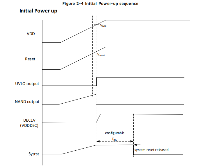
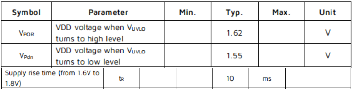
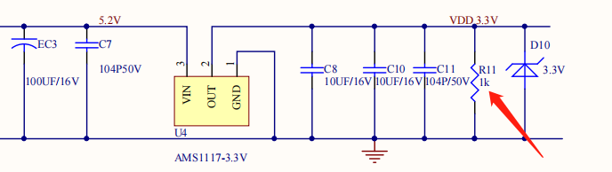
The Z2 chip has requirements on the power-on sequence. During the power-on process, the system starts when the RST pin reaches 1.62V. At this time, the VCC needs to reach more than 1.8V within 10ms. Because the RST pin has the RC link, the VCC of the bare module is much more than 1.8V when the RST reaches 1.62V.
In some cases that the large capacitance in the power driver connected to the Z2 chip module charges or discharges, if the module voltage is not fully discharged below 0.6V, the module will probably crash when it is restarted. It is required that the power supply pin VCC_3.3V of the module needs to be connected with a dummy load of 1K to release power quickly. You can refer to the following figure which shows parts of power-driven links.
Antenna information
Antenna type
ZTLC5 uses a monopole antenna.
Antenna interference reduction
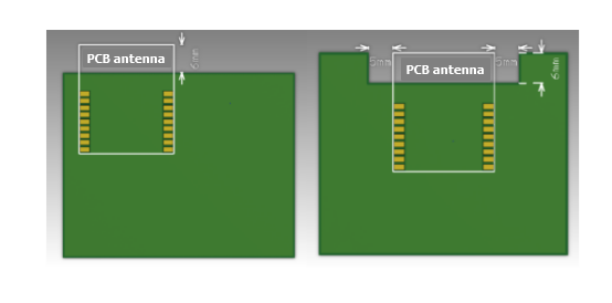
To ensure the optimal Zigbee performance when the Zigbee module uses a monopole antenna, it is recommended that the antenna be at least 15 mm away from other metal parts.
To prevent an adverse impact on the antenna radiation performance, avoid copper or traces along the antenna area on the PCB.
Packaging information and production instructions
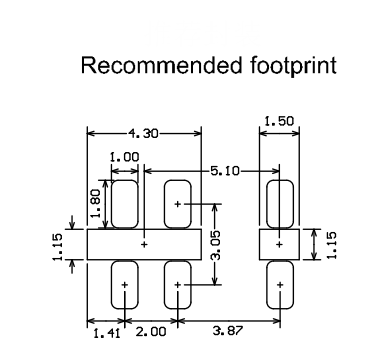
Mechanical dimensions
The PCB dimensions are 12.7±0.35 mm (L)×8.5±0.35 mm (W) ×1.0±0.1 mm (H).
Schematic diagram of footprint
Recommended PCB footprint: In-line manner
ZTLC5 module adopts the in-line manner.
Production instructions
-
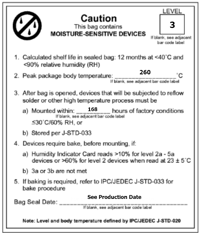
For the Tuya in-line module, wave soldering is most preferred and manual soldering is less preferred. After being unpacked, the module must be soldered within 24 hours. Otherwise, it must be put into the drying cupboard where the RH is not greater than 10%; or it needs to be packaged under vacuum again and record the exposure time (the total exposure time cannot exceed 168 hours).
-
Wave soldering devices and materials:
- Wave soldering equipment
- Wave soldering fixture
- Constant-temperature soldering iron
- Tin bar, tin wire, and flux
- Thermal profiler
-
Baking devices:
- Cabinet oven
- Anti-electrostatic and heat-resistant trays
- Anti-electrostatic and heat-resistant gloves
-
The module needs to be baked in the following cases:
- The packaging bag is damaged before unpacking.
- There is no humidity indicator card (HIC) in the packaging bag.
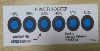
- After unpacking, circles of 10% and above on the HIC become pink.
- The total exposure time has lasted for over 168 hours since unpacking.
- More than 12 months have passed since the sealing of the bag.
-
Baking settings:
- Temperature: 40°C and ≤ 5% RH for reel package and 125°C and ≤5% RH for tray package (please use the heat-resistant tray rather than a plastic container)
- Time: 168 hours for reel package and 12 hours for tray package
- Alarm temperature: 50°C for reel package and 135°C for tray package
- Production-ready temperature after natural cooling: < 36°C
- Re-baking situation: If a module remains unused for over 168 hours after being baked, it needs to be baked again.
- If a batch of modules is not baked within 168 hours, do not use the wave soldering to solder them. Because these modules are Level-3 moisture-sensitive devices, they are very likely to get damp when exposed beyond the allowable time. In this case, if they are soldered at high temperatures, it may result in device failure or poor soldering.
-
In the whole production process, take electrostatic discharge (ESD) protective measures.
-
To guarantee the quality of products, you must pay attention to the following items: The amount of soldering flux, the height of the wave peak, whether the tin slag and copper content in the wave soldering tank exceed standards, whether the window and thickness of the wave soldering fixture are appropriate, and whether the wave soldering oven temperature curve is appropriate.
Recommended oven temperature curve and temperature
Set oven temperatures according to the following temperature curve of wave soldering. The peak temperature is 260°C±5°C.
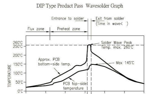
Recommended soldering temperature:
| Suggestions on oven temperature curve of wave soldering | Suggestions on manual soldering temperature | ||
|---|---|---|---|
| Preheat temperature | 80 to 130 °C | Soldering temperature | 360±20°C |
| Preheat time | 75 to 100s | Soldering time | <3s/point |
| Peak contact time | 3 to 5s | NA | NA |
| Temperature of tin cylinder | 260±5°C | NA | NA |
| Ramp-up slope | ≤2°C/s | NA | NA |
| Ramp-down slope | ≤6°C/s | NA | NA |
Storage conditions
Storage conditions for a delivered module:
-
The moisture-proof bag is placed in an environment where the temperature is below 40°C and the relative humidity is lower than 90%.
-
The shelf life of a dry-packaged product is 12 months from the date when the product is packaged and sealed.
-
There is a humidity indicator card (HIC) in the packaging bag.
MOQ and packaging information
| Product model | MOQ (pcs) | Packing method | The number of modules per reel | The number of reels per carton |
|---|---|---|---|---|
| ZTLC5 | 6000 | Tape reel | 1500 | 4 |
Appendix: Statement
FCC Caution: Any changes or modifications not expressly approved by the party responsible for compliance could void the user’s authority to operate this device.
This device complies with Part 15 of the FCC Rules. Operation is subject to the following two conditions: (1) This device may not cause harmful interference, and (2) this device must accept any interference received, including interference that may cause undesired operation.
Note: This device has been tested and found to comply with the limits for a Class B digital device, according to part 15 of the FCC Rules. These limits are designed to provide reasonable protection against harmful interference in a residential installation. This device generates, uses, and can radiate radio frequency energy and, if not installed and used following the instructions, may cause harmful interference to radio communications. However, there is no guarantee that interference will not occur in a particular installation.
If this device does cause harmful interference to radio or television reception, which can be determined by turning the device off and on, the user is encouraged to try to correct the interference by one or more of the following measures:
- Reorient or relocate the receiving antenna.
- Increase the separation between the device and receiver.
- Connect the device into an outlet on a circuit different from that to which the receiver is connected.
- Consult the dealer or an experienced radio/TV technician for help.
Radiation Exposure Statement
This device complies with FCC radiation exposure limits set forth for an uncontrolled rolled environment. This device should be installed and operated with a minimum distance of 20cm between the radiator and your body.
Important Note
This radio module must not be installed to co-locate and operating simultaneously with other radios in the host system except following FCC multi-transmitter product procedures. Additional testing and device authorization may be required to operate simultaneously with other radios.
The availability of some specific channels and/or operational frequency bands are country dependent and are firmware programmed at the factory to match the intended destination. The firmware setting is not accessible by the end-user.
The host product manufacturer is responsible for compliance with any other FCC rules that apply to the host not covered by the modular transmitter grant of certification. The final host product still requires Part 15 Subpart B compliance testing with the modular transmitter installed.
The end-user manual shall include all required regulatory information/warnings as shown in this manual, including "This product must be installed and operated with a minimum distance of 20 cm between the radiator and user body".
This device has got an FCC ID: 2ANDL-ZTLC5. The end product must be labeled in a visible area with the following: "Contains Transmitter Module FCC ID: 2ANDL-ZTLC5".
This device is intended only for OEM integrators under the following conditions:
The antenna must be installed such that 20cm is maintained between the antenna and users, and the transmitter module may not be co-located with any other transmitter or antenna.
As long as the 2 conditions above are met, further transmitter tests will not be required. However, the OEM integrator is still responsible for testing their end-product for any additional compliance requirements required with this module installed.
Declaration of Conformity European Notice

Hereby, Hangzhou Tuya Information Technology Co., Ltd declares that this module product is in compliance with essential requirements and other relevant provisions of Directive 2014/53/EU,2011/65/EU. A copy of the Declaration of conformity can be found at https://www.tuya.com.

This product must not be disposed of as normal household waste, in accordance with the EU directive for waste electrical and electronic equipment (WEEE-2012/19/EU). Instead, it should be disposed of by returning it to the point of sale, or to a municipal recycling collection point.
The device could be used with a separation distance of 20cm to the human body.
Is this page helpful?
YesFeedbackIs this page helpful?
YesFeedback


