LZ2x1 Series Hardware Design Guidelines
These guidelines are intended to serve as the reference when you develop with LZ2x1 series modules. It helps you get an overall understanding of the product specifications and assists in developing IoT products and applications.
This topic describes the hardware design guidelines in terms of features, specifications, reliability tests, test standards, development process, radio frequency (RF) metrics, and circuit designs.
Background
Glossary
| Abbreviation | Spelled-out |
|---|---|
| ESD | Electrostatic discharge |
| USB | Universal serial bus |
| UART | Universal asynchronous receiver-transmitter |
| SIM | Subscriber identification module |
| SPI | Serial peripheral interface |
| I2C | Inter-integrated circuit |
| I/O | Input/Output |
| GPIO | General-purpose input/output |
| TBD | To be determined |
| RTC | Real time clock |
| ADC | Analog-to-digital converter |
References
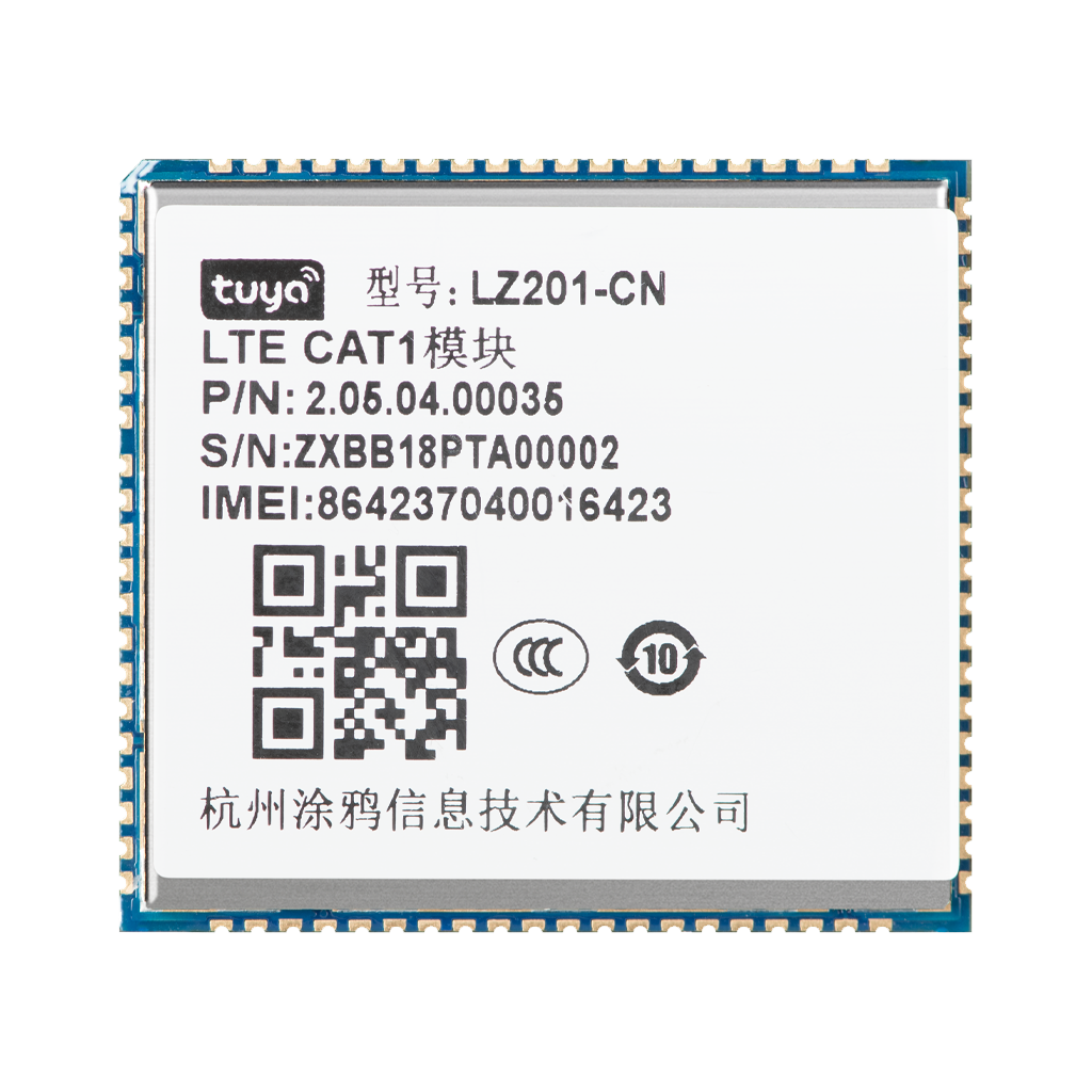
These guidelines apply to LZ2x1 series modules, including LZ201-CN, LZ211-CN, LZ201-EAU, and LZ211-EAU.
- LZ201-CN Datasheet
- LZ211-CN Datasheet
- LZ211-EAU Datasheet
- LZ2x1 Series Hardware Design Guidelines (This documentation)
- LZ2x1 Series Schematic Diagram
- LZ2x1 Series Open CPU GPIO Configuration
- LTE Cat.1 Serial Protocol
Product overview
The LZ2x1 series is a family of LTE Cat.1 cellular modules from Tuya Smart. The LZ2x1 module consists of a highly integrated LTE Cat.1 chip UIS8910DM and peripheral circuits. It has a built-in LTE Cat.1 network communication protocol stack and library functions.
The LZ2x1 module is built around an Arm Cortex-A5 processor and Cat.1 bis modem and embedded with 64 MB NOR flash and 128 MB PSRAM. It provides a wide array of interfaces including USB, UART, SDIO, SPI, I2C, I2S, and ADC for supporting peripherals such as the display, camera, keyboard matrix circuit, microphone, speaker, charger, microSD card, and USIM card.
Models
| Frequency bands | LZ201-CN | LZ211-CN | LZ201-EAU | LZ211-EAU |
|---|---|---|---|---|
| LTE FDD | Band 1, 3, 5, 8 | Band 1, 3, 5, 8 | Band 1, 3, 5, 7, 8, 20, 28A | Band 1, 3, 5, 7, 8, 20, 28A |
| LTE TDD | Band 34, 38, 39, 40, 41 | Band 34, 38, 39, 40, 41 | Band 38, 40, 41 | Band 38, 40, 41 |
| GSM | Not supported | Not supported | 900/1800 | 900/1800 |
| GNSS | Not supported | Support | Not supported | Support |
| Bluetooth Low Energy 4.2 | Support | Support | Not supported | Not supported |
| Wi-Fi Scan | Support | Support | Not supported | Support |
Features
- 1 Within the operation temperature range, the module is 3GPP compliant.
- 2 Within the extended temperature range, the module remains the ability to operate properly. Only the values of one or more parameters like output power might exceed the specified tolerances of 3GPP specifications.
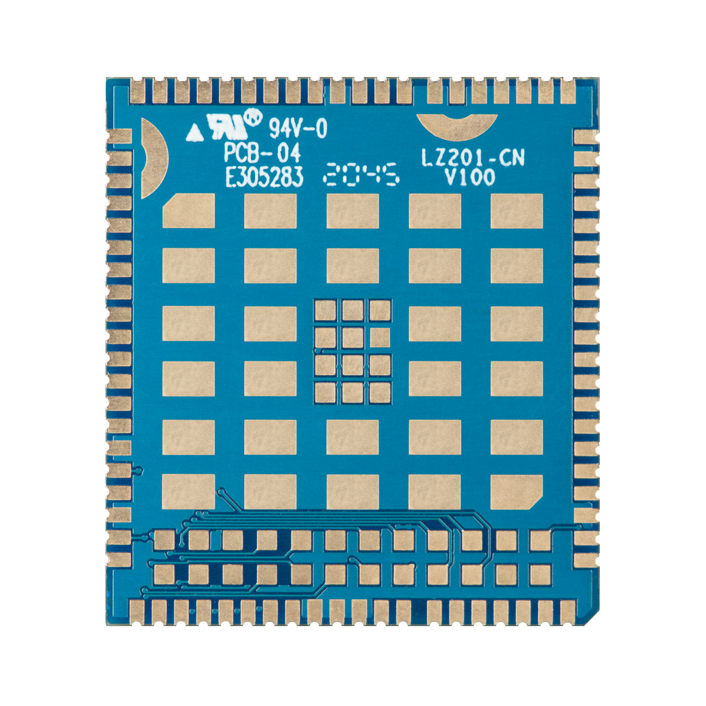
Appearance
Pin configuration and functions
LZ2x1 is equipped with a total of 144 pins, including 80 LCC pins and 64 LGA pins.
The pinout is as follows:
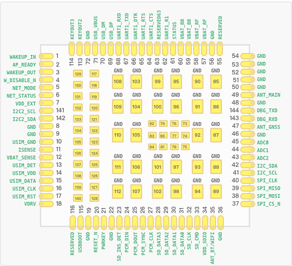
I/O parameters definition
| Type | Description |
|---|---|
| P | Power supply |
| I | Input |
| O | Output |
| IO | Input/Output |
Pin description
| Pin No. | Pin name | I/O type | Description |
|---|---|---|---|
| 1 | WAKEUP_IN | I | External circuit wakes up the module. It can be used as GPIO10 in OpenCPU mode. If it is unused, keep it open. |
| 2 | AP_READY* | I | Used to inform the module whether the application processor is in sleep mode. It can be used as GPIO11 in OpenCPU mode. If it is unused, keep it open. |
| 3 | WAKEUP_OUT* | O | The module wakes up the external circuit. It can be used as GPIO5 in OpenCPU mode. If it is unused, keep it open. |
| 4 | W_DISABLE_N* | I | Used to force the module into airplane mode. It can be used as GPIO8 in OpenCPU mode. If it is unused, keep it open. |
| 5 | NET_MODE | PI | Indicate the module’s network registration mode, which applies when the module operates in self-processing mode. NET_MODE is a current source and connected to the LED GND pin. |
| 6 | NET_STATUS* | O | Indicate the module network activity status. It can be used as GPIO9 in OpenCPU mode. |
| 7 | VDD_EXT | PO | 1.8V voltage output. It can provide pull-up for the external circuit. If it is unused, keep it open. |
| 8 | GND | - | The ground pin. |
| 9 | GND | - | The ground pin. |
| 10 | USIM_GND | - | The ground pin. It shares the same network as GND. |
| 11 | ISENSE | I | Measure the charge current. |
| 12 | VBAT_SENSE | I | Measure battery voltage. Connect it close to the positive terminal of batteries to sense the battery voltage. If the battery is not used, disable low voltage shutdown in the software. Otherwise, the module will shut down on low voltage. |
| 13 | USIM_DET | I | USIM card hot-plug detection, which is disabled by default in the software. Pull this pin up to VDD_EXT. |
| 14 | USIM_VDD | PO | Power supply for the USIM card. Either 1.8V or 3.0V is supported by the module automatically. |
| 15 | USIM_DATA | IO | Data signal of USIM card. |
| 16 | USIM_CLK | O | USIM card clock signal. |
| 17 | USIM_RST | O | Reset signal of the USIM card. |
| 18 | VDRV | O | Enable the charger circuit. |
| 19 | GND | - | The ground pin. |
| 20 | RESET_N | I | Reset the module. Active low. |
| 21 | PWRKEY | I | Power on or off the system. |
| 22 | GND | - | The ground pin. |
| 23 | SD_INS_DET | I | SD card insertion detection. It can be used as GPIO7 in OpenCPU mode. |
| 24 | PCM_DIN | I | PCM data input. It can be used as GPIO2 in OpenCPU mode. |
| 25 | PCM_DOUT | O | PCM data output. It can be used as GPIO3 in OpenCPU mode. |
| 26 | PCM_SYNC | IO | PCM data sync. It can be used as GPIO1 in OpenCPU mode. |
| 27 | PCM_CLK | IO | PCM audio clock signal. It can be used as GPIO0 in OpenCPU mode. |
| 28 | SD_DATA3 | I | SD card SDIO data bit 3. It can be used as WLAN SDIO. |
| 29 | SD_DATA2 | I | SD card SDIO data bit 2. It can be used as WLAN SDIO. |
| 30 | SD_DATA1 | I | SD card SDIO data bit 1. It can be used as WLAN SDIO. |
| 31 | SD_DATA0 | I | SD card SDIO data bit 0. It can be used as WLAN SDIO. |
| 32 | SD_CLK | O | SD card SDIO clock signal. It can be used as WLAN SDIO. |
| 33 | SD_CMD | IO | SD card SDIO command signal. It can be used as WLAN SDIO. |
| 34 | VDD_SDIO | PO | Power supply for SD card. It can be used as WLAN SDIO. |
| 35 | ANT_BT/WIFI | AIO | Bluetooth and Wi-Fi antenna. |
| 36 | GND | - | The ground pin. |
| 37 | SPI_CS_N | I | SPI chip select |
| 38 | SPI_MOSI | I | SPI MOSI |
| 39 | SPI_MISO | O | SPI MISO |
| 40 | SPI_CLK | O | SPI clock signal |
| 41 | I2C_SCL | OD | I2C clock signal. It can be used as GPIO14 in OpenCPU mode. |
| 42 | I2C_SDA | OD | I2C data signal. It can be used as GPIO15 in OpenCPU mode. |
| 43 | ADC2 | AI | Analog to digital converter interface 2. |
| 44 | ADC1 | AI | Analog to digital converter interface 1. |
| 45 | ADC0 | AI | Analog to digital converter interface 0. |
| 46 | GND | - | The ground pin. |
| 47 | ANT_GNSS | AI | GNSS antenna, supported by LZ211 series and not supported by LZ201 series. |
| 48 | GND | - | The ground pin. |
| 49 | ANT_MAIN | AIO | Main antenna interface. |
| 50 to 54 | GND | - | The ground pin. |
| 55 | RESERVED | - | Reserved |
| 56 | GND | - | The ground pin. |
| 57 | VBAT_RF | P | Power supply for module RF part. Supply voltage: 3.4V to 4.3V. Nominal voltage: 3.8V. Peak current: 2A. |
| 58 | VBAT_RF | P | Power supply for module RF part. Supply voltage: 3.4V to 4.3V. Nominal voltage: 3.8V. Peak current: 2A. |
| 59 | VBAT_BB | P | Power supply for baseband part. Supply voltage: 3.4V to 4.3V. Nominal voltage: 3.8V. Current: 1A. |
| 60 | VBAT_BB | P | Power supply for baseband part. Supply voltage: 3.4V to 4.3V. Nominal voltage: 3.8V. Current: 1A. |
| 61 | STATUS* | O | Module status output. |
| 62 | UART1_RI* | O | Ring indicator. It can be used as GPIO12 in OpenCPU mode. |
| 63 | RESERVED63 | O | Reserved |
| 64 | UART1_CTS | O | UART 1 clear to send. It can be used as GPIO18 in OpenCPU mode. |
| 65 | UART1_RTS | I | UART 1 request to send. It can be used as GPIO19 in OpenCPU mode. |
| 66 | UART1_DTR* | I | Wake up the module. |
| 67 | UART1_TXD | O | UART 1 transmit data. It can be connected to an external MCU. |
| 68 | UART1_RXD | I | UART 1 receive data. It can be connected to an external MCU. |
| 69 | USB_DP | IO | USB high-speed differential transceiver (positive). It can be used to download code to the module. |
| 70 | USB_DM | IO | USB high-speed differential transceiver (negative). It can be used to download code to the module. |
| 71 | USB_VBUS | PI | Detect USB insertion. |
| 72 | GND | - | The ground pin. |
| 73 | SPK_P | O | Speaker output signal (positive). |
| 74 | SPK_N | O | Speaker output signal (negative). |
| 75 | MIC_P | I | Microphone input signal (positive). |
| 76 | GND | - | The ground pin. |
| 77 | MIC_N | I | Microphone input signal (negative). |
| 78 | KEYIN1 | IO | Key input 1. |
| 79 | KEYIN2 | IO | Key input 2. |
| 80 | KEYIN3 | IO | Key input 3. |
| 81 | KEYIN4 | IO | Key input 4. |
| 82 | KEYIN5 | IO | Key input 5. |
| 83 | KEYOUT0 | IO | Key output 0. |
| 84 | KEYOUT1 | IO | Key output 1. |
| 85 to 112 | GND | - | The ground pin. |
| 113 | KEYOUT2 | IO | Key output 2. |
| 114 | KEYOUT3 | IO | Key output 3. |
| 115 | USBBOOT | IO | Key input 0. Pulling up this pin to VDD_EXT before power-on will make the module enter USB download mode. Leaving this pin floating will boot the module in normal mode. |
| 116 | RESERVED116 | - | Reserved. Keep it open. |
| 117 | CLK26M_OUT* | O | 26M clock signal. |
| 118 | RESERVED118 | - | Reserved. Keep it open. |
| 119 | LCD_FMARK | O | SPI LCD frame sync signal |
| 120 | LCD_RSTB | O | SPI LCD reset signal |
| 121 | LCD_SEL | O | SPI LCD selection |
| 122 | LCD_CS | O | SPI LCD chip select |
| 123 | LCD_CLK | O | SPI LCD clock signal |
| 124 | LCD_SDC | O | SPI LCD data command selection |
| 125 | LCD_SIO | O | SPI LCD data signal |
| 126 | VDDLCD | P | External LCD power supply |
| 127 | PM_ENABLE | O | External power LDO control. It can be used as GPIO13 in OpenCPU mode. |
| 128 | VDDCAMA | P | Power supply for camera VCAMA |
| 129 | CAM_PWDN | IO | Camera CAM_PWDN signal |
| 130 | CAM_SI1 | IO | Camera CAM_SI1 signal |
| 131 | CAM_SI0 | IO | Camera CAM_SI0 signal |
| 132 | CAM_RSTL | IO | Camera CAM_RSTL signal |
| 133 | CAM_REFCLK | O | Camera CAM_REFCLK signal |
| 134 | CAM_SCK | IO | Camera CAM_SCK signal |
| 135 | UART2_RXD/WAKE_WLAN | O | UART 2 receive data. It can be used for the external Wi-Fi module to wake up the LZ201* module or used as GPIO20 in OpenCPU mode. Downloading code to the module is supported. |
| 136 | UART2_TXD/WLAN_EN | O | UART 2 transmit data. It can be used to enable the external Wi-Fi module* or used as GPIO21 in OpenCPU mode. Downloading code to the module is supported. |
| 137 | UART3_RXD/KEYOUT4 | I | UART 3 receive data. It can be used as KEYOUT4. |
| 138 | UART3_TXD/KEYOUT5 | O | UART 3 transmit data. It can be used as KEYOUT5. |
| 139 | ZSP_UART_TXD/BT_EN | O | ZSP log output. It can be used to enable the external Bluetooth Low Energy mesh module* or used as GPIO22 in OpenCPU mode. |
| 140 | VDDCAMD | P | Power supply for camera VCAMD |
| 141 | I2C2_SCL | IO | I2C clock signal. |
| 142 | I2C2_SDA | IO | I2C data signal. It can be used as GPIO17 in OpenCPU mode. |
| 143 | DBG_RXD | I | Debugging interface, used for the module to receive data. |
| 144 | DBG_TXD | O | Debugging interface, used for the module to transmit data. |
Pindicates the power pin.I/Oindicates the input and output pin.*indicates this feature is not supported currently.
Power supply
Power and ground pins
LZ2X1 can be powered by a battery or an external power supply. The ground pin and signal ground pin must be connected to the ground plane on the PCB. Otherwise, the overall performance of the module might be affected.
| Pin No. | Signal | Description | Min | Typical | Max | Unit |
|---|---|---|---|---|---|---|
| 59 and 60 | VBAT_BB | Power supply for the baseband part. | 3.4 | 3.8 | 4.3 | V |
| 57 and 58 | VBAT_PA | Power supply for the RF part. | 3.4 | 3.8 | 4.3 | V |
| 8, 9, 10, 19, 22, 36, 46, 48, 50-54, 56, 72, 76, 85-112 | GND | GND | - | - | - | - |
Power supply requirements
-
The supply voltage of the LZ2X1 module ranges from 3.4V to 4.3V, with a peak current of 2A.
- If the difference between the input and output voltage is small, you can use a low-dropout (LDO) regulator to maintain the required system voltage.
- If the difference between the input and output voltage is large, you can use a DC-to-DC converter to regulate the output voltage.
-
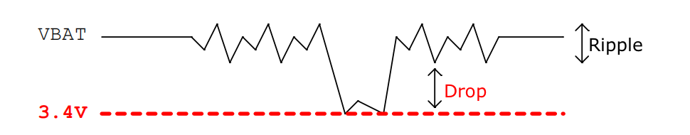
Voltage drop: When the module is working, make sure its input voltage will never drop below 3.4V and the ripple voltage is less than 300 mV.
-
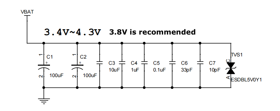
Voltage regulator and filter capacitor:
- Capacitors used for the voltage regulation circuit of a power supply: 100 μF × 2, 10 μF
- Filter capacitors on digital signals: 1 μF, 0.1 μF
- Filter capacitors on high-frequency signals: 33 pF, 10 pF
-
Electrostatic discharge protection: Add a TVS diode on the VBAT trace (near VBAT pins) to improve surge voltage withstand capability.
-
In principle, star routing topology is required. The longer the VBAT trace is, the wider it should be.
-
If the module is powered by a battery, you can enable low voltage (less than 3.38V) shutdown, with consideration of the power of other components on the backplane. Otherwise, the module might not be powered on due to battery over-discharge.
A reference circuit for the power supply is illustrated in the following figure.
Power on/reset
Pin description
| Pin No. | Signal | Description |
|---|---|---|
| 21 | PWRKEY | Power on the module. |
| 20 | RESET_N | Reset the module. |
Applications
-
Power on: The module will be powered on after the
PWRKEYpin is driven to a low level for at least 1.5 seconds and then pulled up or left floating.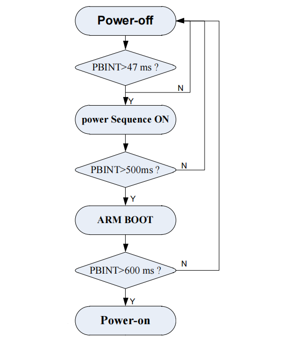
-
Auto power-on: If you want the module to be powered on whenever a power source is connected and do not need the shutdown feature, you can pull down
PWRKEYto ground. -
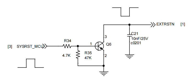
Reset: The module will be reset after the
RESETpin is driven to a low level for at least 35 ms and then pulled up or left floating.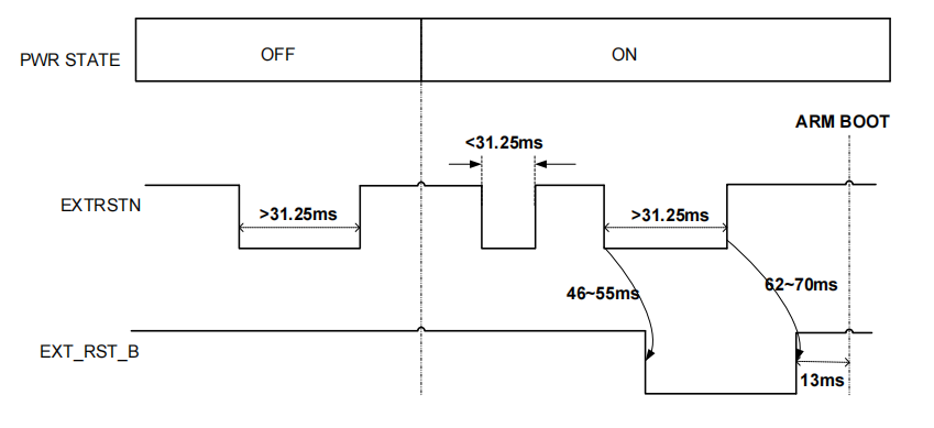
-
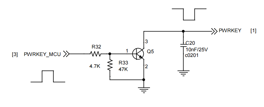
An open drain/collector driver is recommended, as shown in the following schematics.
- Power-on circuit
- Reset circuit
UART interface
Pin description
The module provides three UART interfaces:
-
UART 1: used to connect to your MCU. The serial data transmission follows Tuya’s protocol. The baud rate is 115200 bps by default.
-
UART 2: used to connect to peripheral devices. For modules with the GNSS feature, this interface has been occupied by the internal GNSS chip.
-
UART 3: used to connect to peripheral devices.
Pin No. Signal Description 68 UART1_RXD UART 1 receive data. 67 UART1_TXD UART 1 transmit data. 64 UART1_CTS UART 1 clear to send. 65 UART1_RTS UART 1 request to send. 135 UART2_RXD UART 2 receive data. 136 UART2_TXD UART 2 transmit data. 137 UART3_RXD UART 3 receive data. 138 UART3_TXD UART 3 transmit data.
Applications
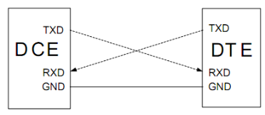
The module provides 1.8V UART interfaces. A level translator should be used if the application is equipped with a 3.3V or 5V UART interface. As shown in the following figure:
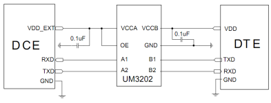
Alternatively, use a triode to translate voltage levels.
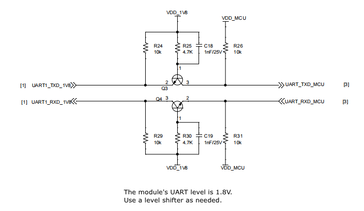
See the circuit diagram above for how UART 1, UART 2, and UART 3 are connected.
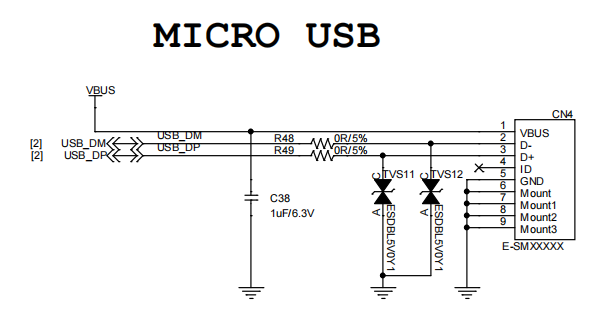
USB interface
Pin description
The USB interface conforms to USB 2.0 specifications and can be used to download code to the module.
For all your projects, it is strongly recommended to reserve a USB port for program download and debugging.
| Pin No. | Signal | Description |
|---|---|---|
| 69 | USB_DP | USB high-speed differential transceiver (positive). It can be used to download code to the module. |
| 70 | USB_DM | USB high-speed differential transceiver (negative). It can be used to download code to the module. |
| 71 | USB_VBUS | Data signal of USIM card. |
| 115 | USBBOOT | Pulling up this pin to VDD_EXT before power-on will make the module enter USB download mode. Leaving this pin floating will boot the module in normal mode. |
Applications
-
MCU solutions
-
Micro-USB cable
Circuit design
-
Pull up
USBBOOTtoVDD_EXTto boot the module in USB download mode. -
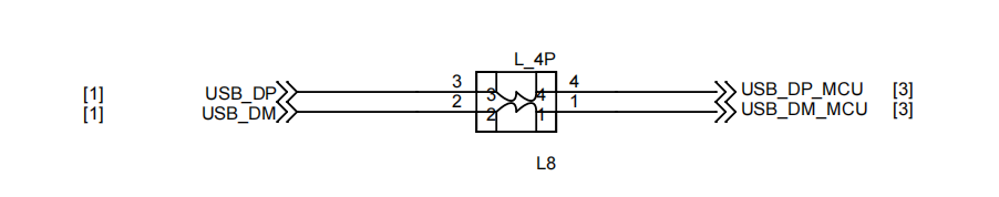
Make sure to route the USB signal traces as differential pairs with total grounding. The impedance of USB differential trace is 90Ω.
-
Do not route signal traces under the power supply, RF signal traces, and other sensitive signal traces. It is important to route the USB differential traces in the inner layer with ground shielding on not only the upper and lower layers but also the right and left sides.
-
Connect a common mode choke between the MCU and module in series to improve EMI suppression.
-
VBUSis used to detect the presence of the USB bus. If the USB port on your MCU does not support the suspend mode, you can disconnectVBUSto make the module enter sleep mode.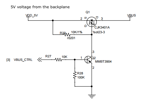
-
Considering connection to micro-USB devices, place the TVS diode as close to the USB port as possible with a parasitic capacitance of less than 2 pF.
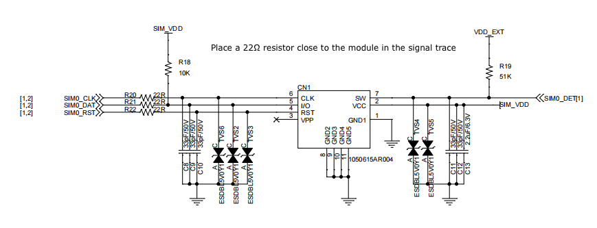
SIM card interface
Pin description
| Pin No. | Signal | Description |
|---|---|---|
| 13 | USIM_DET | USIM card hot-plug detection, which is disabled by default in the software. Pull this pin up to VDD_EXT. |
| 14 | USIM_VDD | Power supply for USIM card. Either 1.8V or 3.0V is supported by the module automatically. |
| 15 | USIM_DATA | Data signal of USIM card. |
| 16 | USIM_CLK | USIM card clock signal. |
| 17 | USIM_RST | Reset signal of the USIM card. |
Applications
Circuit design
- Place the SIM card connector near the module. Keep the trace length as less than 200 mm as possible.
- Place a 2.2 μF decouple capacitor between
USIM_VDDand GND, close to the SIM card connector. - Place a 10 to 20K pull-up resistor on the
USIM_DATAto reduce EMI. - Place the RF bypass capacitors (33 pF) close to the SIM card connector on all signal traces (
USIM_DATA,USIM_RST, andUSIM_CLK) to improve EMI suppression. - Keep USIM card signals away from RF and VBAT traces. To avoid crosstalk between
SIM_DATAandSIM_CLK, keep them away from each other. - In order to offer good ESD protection, it is recommended to add a TVS diode array with a parasitic capacitance of less than 15 pF. The ESD protection device should be placed as close to the SIM card connector as possible, and make sure the SIM card signal lines go through the ESD protection device first and then to the module.
- For the design of SIM card hot-swapping, the
USIM_DETis shorted to the ground when no card is inserted. When a card is inserted,USIM_DETfloats and is pulled up byVDD_EXT. If you do not useUSIM_DET, pull it up toVDD_EXT.
SD card interface
Pin description
The memory card interface provides access to memory cards compliant with SD 2.0 and SDIO 1.1 standards.
| Pin No. | Signal | Description |
|---|---|---|
| 28 | SD_DATA3 | SD card SDIO data bit 3. |
| 29 | SD_DATA2 | SD card SDIO data bit 2. |
| 30 | SD_DATA1 | SD card SDIO data bit 1. |
| 31 | SD_DATA0 | SD card SDIO data bit 0. |
| 32 | SD_CLK | SD card SDIO clock signal. |
| 33 | SD_CMD | SD card SDIO command signal. |
| 34 | VDD_SDIO | SD card SDIO bus pull-up power. |
Applications
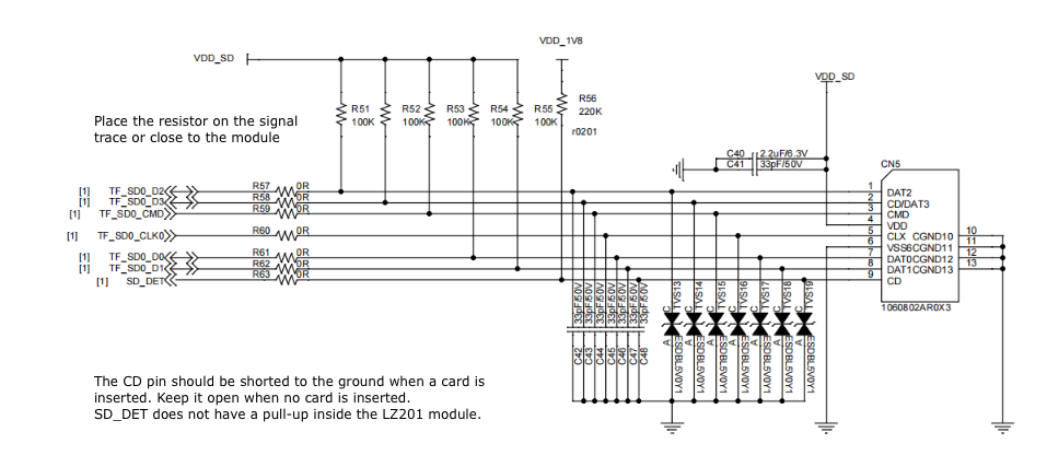
Circuit design
- The maximum output current of
VDD_SDIOis 150 mA. If the SD card current consumption exceeds 150 mA, an external power supply is needed. - Connect a 22Ω resistor between the
SD_CLKand SD signal trace in series to reduce EMI. - Reserve a pad for 0201 33 pF capacitor on the signal trace.
- Reserve a pad for a pull-up resistor (100 kΩ is recommended) on the SD signal trace for increasing the stability of the bus line.
VDD_SDIOis the pull-up power supply. SD_CLKneeds ground shielding. Surround SD signal traces with total grounding to prevent any possible crosstalk and noise coupling from other signal sources.- It is recommended to keep the same trace length for
SD_CLK,SD_DATA[0:3], andSD_CMD, with a length difference of less than 1 mm. The total length should not exceed 50 mm. - In order to offer good ESD protection, it is recommended to add a TVS diode array with a parasitic capacitance of less than 15 pF. The ESD protection device should be placed as close to the SIM card connector as possible, and make sure the SIM card signal lines go through the ESD protection device first and then to the module.
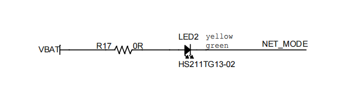
Network status indication
Pin description
| Pin No. | Signal | Description |
|---|---|---|
| 5 | NET_MODE | Indicate the module’s network registration mode, which applies when the module operates in self-processing mode. NET_MODE is a current source and connected to the LED GND pin. |
Applications
- Status indication is disabled by default. The module reports the network status to the MCU through the serial port. To turn on status indication, you need to enable self-processing mode in the software.
NET_MODEis the current source so it should be connected to the negative terminal of the LED.
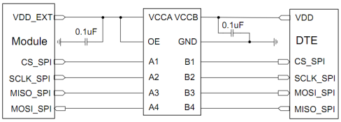
SPI interface
Pin description
| Pin No. | Signal | Description |
|---|---|---|
| 37 | SPI_CS_N | SPI chip select |
| 38 | SPI_MOSI | Controller out and agent in |
| 39 | SPI_MISO | Controller in and agent out |
| 40 | SPI_ SCLK | SPI serial clock signal |
Applications
The module provides 1.8V SPI interface. A level translator should be used if the application is equipped with a 3.3V UART interface.
A reference circuit is illustrated in the following figure.
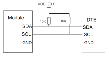
I2C bus
Pin description
| Pin No. | Signal | Description |
|---|---|---|
| 41 | I2C_SCL | I2C serial clock line |
| 42 | I2C_SDA | I2C serial data line |
I2C is a simple serial communication bus protocol that uses just two bus wires, a serial data wire (SDA) and a serial clock wire (SCL). I2C is integrated into many ICs and allows devices to communicate directly with each other. Each device is recognized by a unique address to differentiate from other devices on the same I2C bus and can operate either as a transmitter or a receiver depending on its function.
Applications
The I2C bus must be pulled up to VDD_EXT.
PCM interface
Pin description
| Pin No. | Signal | Description |
|---|---|---|
| 24 | PCM_DIN | PCM audio input |
| 25 | PCM_DOUT | PCM audio output |
| 26 | PCM_SYNC | PCM audio sync |
| 27 | PCM_CLK | PCM audio clock signal |
Applications
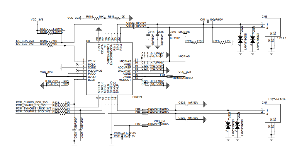
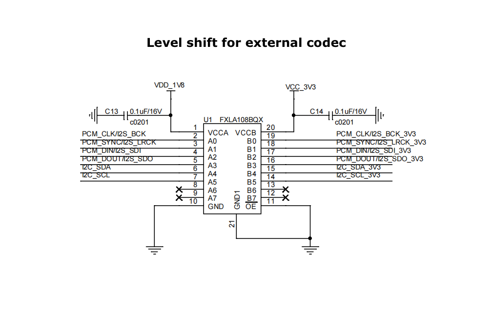
The PCM and I2C are 1.8V. If the codec chip is 3.3V, a level converter is required.
SPI flash interface
The module has a built-in 64 MB NOR flash. If it is not sufficient for your applications, you can add an external SPI flash. This interface can be reused as SPI LCD.
Pin description
| Pin No. | Signal | Description |
|---|---|---|
| 119 | LCD_FRAMK | Reuse SPI flash 1 serial data3 |
| 121 | LCD_SEL | Reuse SPI flash 1 serial data2 |
| 122 | LCD_CS | Reuse SPI flash 1 serial data1 |
| 123 | LCD_CLK | Reuse SPI flash 1 serial data0 |
| 124 | LCD_SDC | Reuse SPI flash 1 CS |
| 125 | LCD_SIO | Reuse SPI flash 1 clock |
Applications
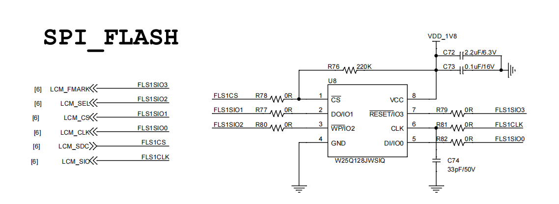
For more information about the supported flash models, see the embedded development documentation.
Charger interface
| Pin No. | Signal | Description |
|---|---|---|
| 11 | ISENSE | Measure the charge current. |
| 12 | VBAT_SENSE | Measure battery voltage. Connect it close to the positive terminal of batteries to sense the battery voltage. If the battery is not used, disable low voltage shutdown in the software. Otherwise, the module will shut down on low voltage. |
| 18 | VDRV | Enable the charger circuit. |
| 71 | USB_VBUS | Detect charging voltage input. |
Applications
-
Linear charger circuit diagram:
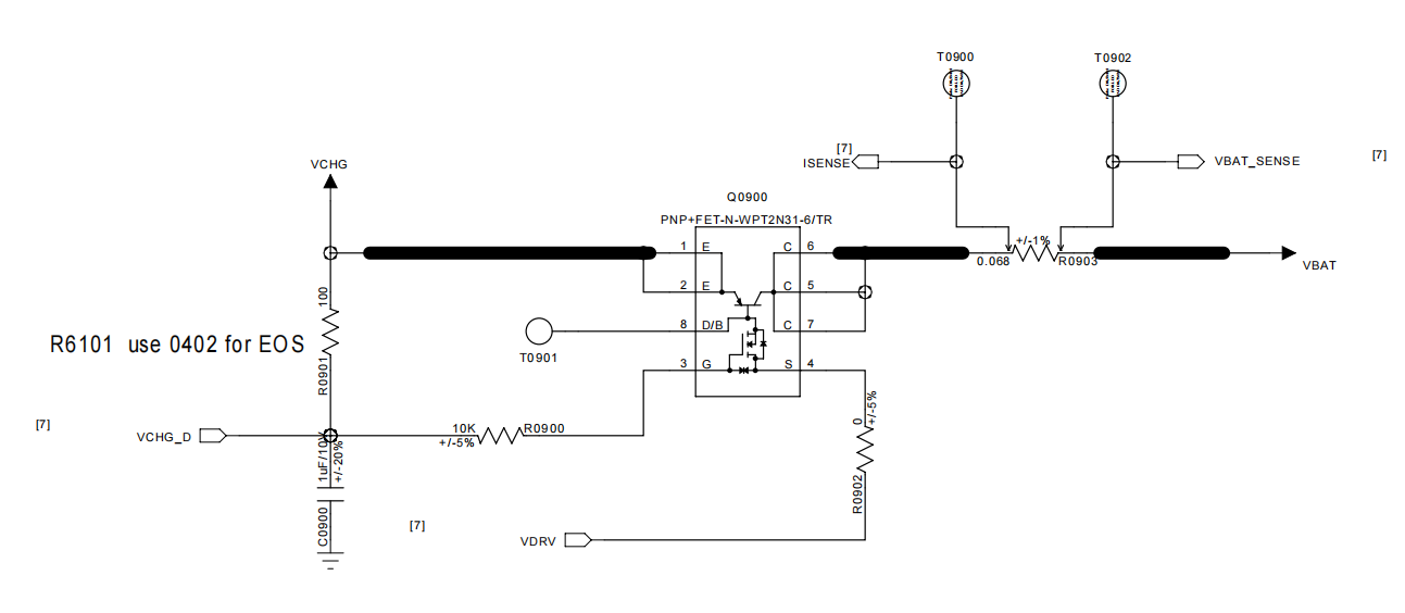
-
Discrete component circuit diagram:
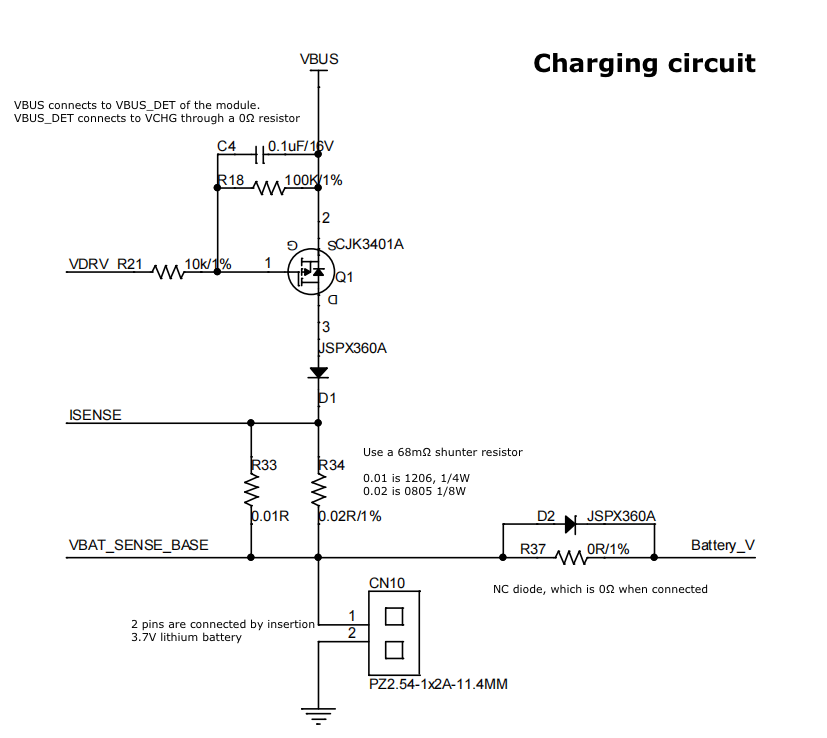
Circuit design
- Considering the thermal design, you can use a linear charger if the charge current is less than 0.7A. Otherwise, switching chargers are recommended.
- To get an accurate charging current,
ISENSEandVBAT_SENSEcan be routed as a pseudo-differential mode (0.075 mm/0.075 mm/0.075 mm). Route the differential traces with ground shielding on the right and left sides. - Place the shunt resistor (0.068Ω±1%, 0.125W, 0805) close to the PNP triode. The trace width of the charger should not be less than 1 mm. The 4-Pin Land Pattern Design from UNISOC is recommended.
- The copper pour for the anode (collector) of the PNP triode should not be less than 30 mm². It is recommended to connect the adjacent layers to the ground for better heat dissipation.
- You can add an NTC thermistor within 1.5 mm around the PNP component to control temperature.
GPIO interface
Some pins can be used as GPIOs if the module uses open CPU SDK-based firmware.
For more information, see LZ2x1 Series Open CPU GPIO Configuration.
Antenna
Pin description
| Pin No. | Signal | Description |
|---|---|---|
| 35 | ANT_BT/WIFI | Bluetooth Low Energy or Wi-Fi antenna |
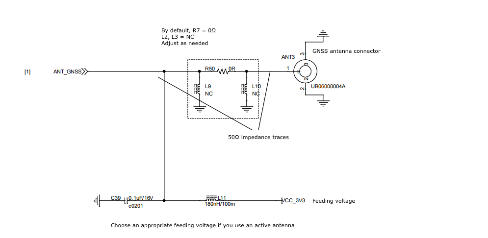
| 47 | ANT_GNSS | GNSS antenna, supported by LZ211 and not supported by LZ201. |
| 49 | ANT_MAIN | LTE antenna |
Antenna matching circuit
In order to achieve better RF performance, it is recommended to place the π-type matching components as close to the antenna as possible.
By default, the capacitors (C1/C2) are not mounted and a 0Ω resistor is mounted on L1.
-
LTE, Bluetooth Low Energy, and Wi-Fi antennas as well as GNSS passive antennas
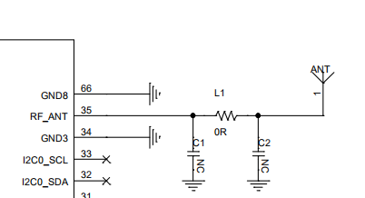
-
GNSS passive/active antennas
Select a passive or active antenna as needed. If you use an active antenna, choose an appropriate feeding voltage based on the antenna datasheet.
RF layout
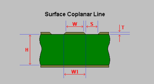
For MCU PCB, the characteristic impedance of all RF traces should be controlled as 50Ω. A microstrip line is used for impedance control.
Microstrip line design on PCB
Principles in RF layout design:
- The distance between the RF pins and the RF connector should be as short as possible. All the right angle traces should be changed to 135° or curved ones.
- The reference ground of RF traces should be complete. Add some ground vias around RF traces. The distance between the ground vias and RF traces should be no less than two times the width of RF signal traces.
- The GND pins are adjacent to RF pins and should be fully connected to the ground.
- There should be a distance between the pad connected to the signal pin and the ground plane.
- Use impedance simulation tool to control the characteristic impedance of RF traces as 50Ω.
- If you use an external antenna, add a TVS diode to prevent ESD damage. The TVS diode’s junction capacitance (Cj in pF) should be less than 0.5 pF.
The following figure provides parameters used for impedance control. You can adjust the trace width properly to get the trace impedance closer to 50Ω.
Antenna design requirements
- The antenna should be kept away from components that are more likely to generate EMI, such as power source and data line.
- To maximize the RF performance, the distance between the antenna and the PCB or mental materials should be at least 15 mm.
- Make sure that the enclosure surrounding the antenna is not metal materials. Otherwise, the radiation performance might be degraded. It is recommended to hollow out the breakout board around the antenna area.
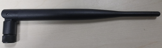
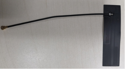
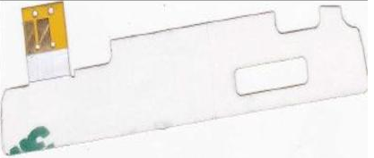
Antenna types
This module does not come with an antenna, so an external antenna is required. You can choose one from the external rubber antenna, helical antenna, FPC antenna with IPEX connector, and PCB antenna. The antenna type can be monopole, planar inverted-F antenna (PIFA), inverted-F antenna (IFA), loop, and more.
The following figure shows the common antennas.
-
Rubber antenna
-
FPC antenna with IPEX connector
-
Built-in FPC antenna
-
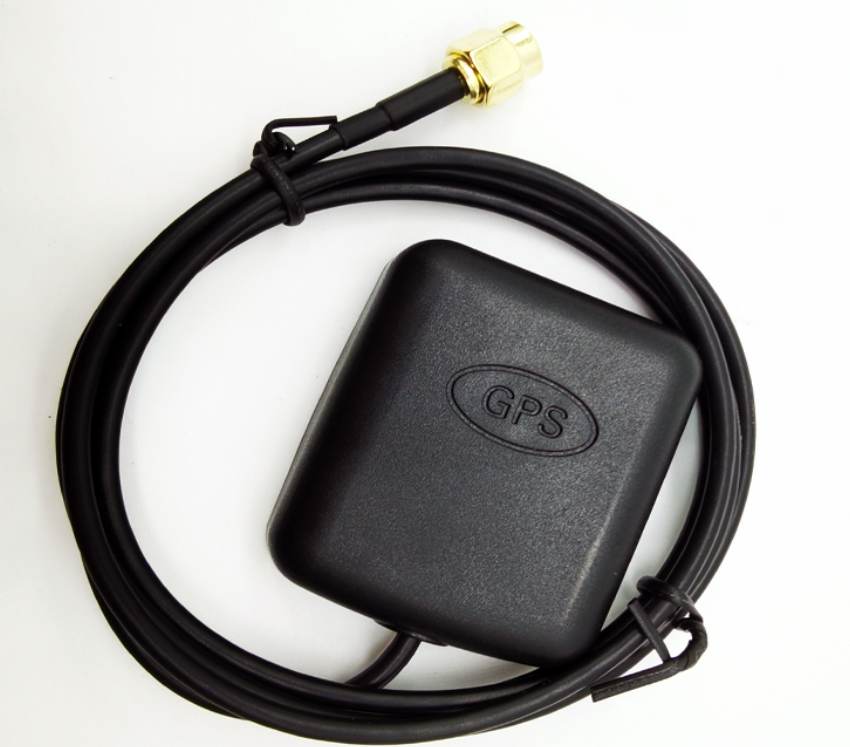
GPS antenna
Adopt an active antenna by adding an external power source.
-
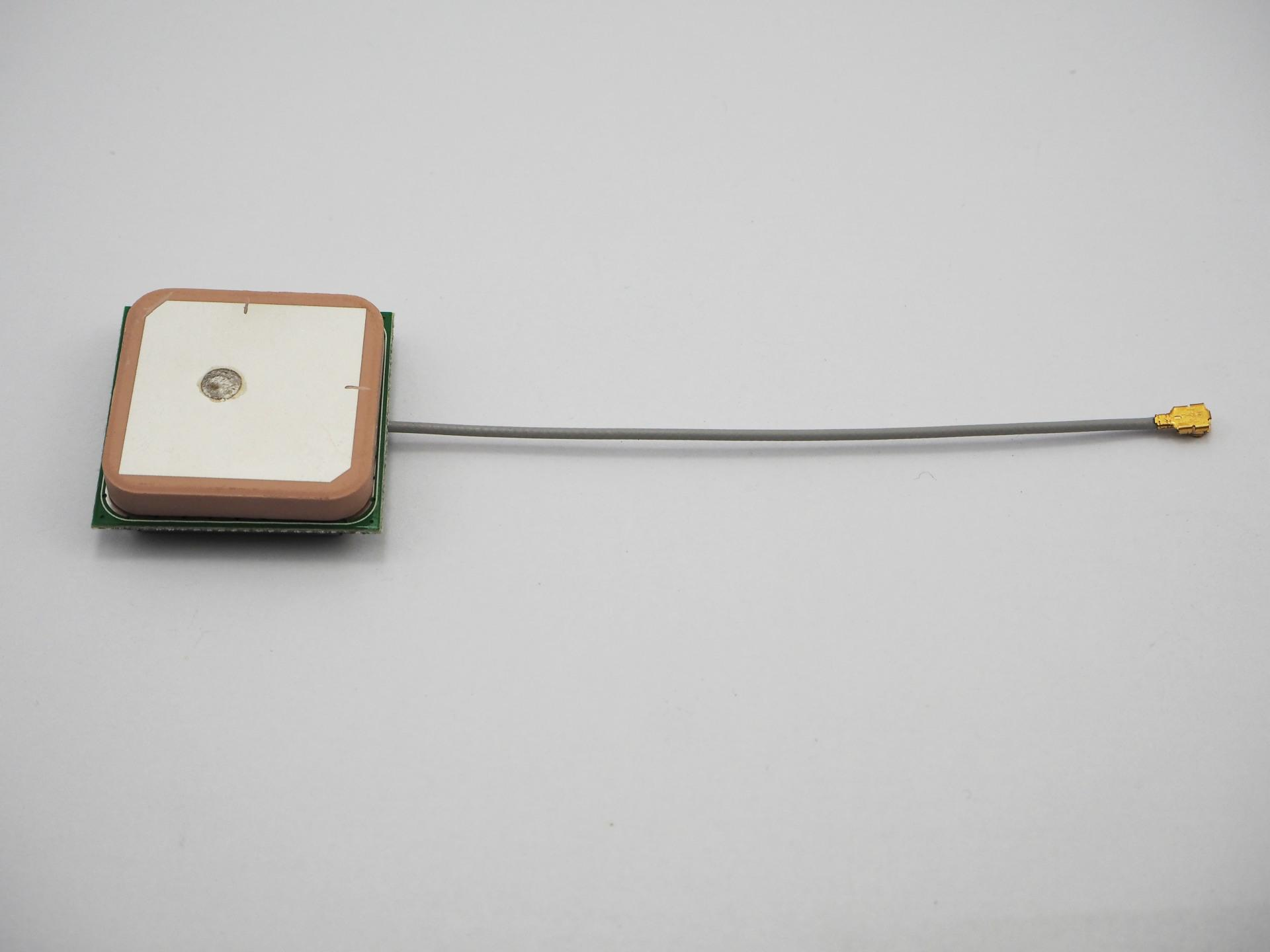
Ceramic GPS antenna
-
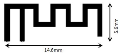
PCB antennas for Bluetooth
Reliability design
EMC and ESD suppression design guide
Electromagnetic compatibility (EMC) is one of the essential considerations in designing for signal integrity and power integrity.
- When you design the peripheral circuit, have two times the width of the trace when routing signals close to each other to minimize noise coupling and generation.
- Place decoupling capacitors close to voltage pins. Keep the high-frequency and high-speed circuits and sensitive circuits away from the edge of the PCB. To reduce crosstalk between signals, increase the spacing between the traces. Provide shielding for components that emit RFI and EMI waves to protect sensitive signals from interference.
Design considerations for ESD circuit protection.
- Place ESD protection devices close to the critical signal I/Os, such as the SIM card, USB port, and TF card.
- In PCB layout and design, make sure the metal shielding enclosure is fully connected to the ground.
PCB pad design
It is recommended to design the 64 pads placed in the middle of the PCB as per the dimensions specified in the structure diagram. Extend the 80 pads around the PCB to the module for over 0.3 mm and the other three sides of the pads for 0.05 mm.
Thermal design
The module generates heat when it works or might be affected by high-temperature components. The module design ensures good heat dissipation. When connecting the module to the PCB, connect the thermal pad to the ground properly to ensure thermal conduction and balance and better electrical performance.
-
Place the module away from the power supply and high-speed signals and protect the traces of sources of EMI.
-
Place the antenna and the coaxial cable that is used to connect the antenna and network interface controller (NIC) away from these sources of EMI.
-
Place the module away from components that generate a large amount of heat such as the CPU. Otherwise, the RF performance might be degraded.
Packing and manufacturing
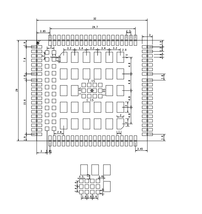
Mechanical dimensions
The dimensions are 29 mm±0.35 (W) × 32 mm±0.35 (L) × 2.4 mm±0.15 (H), as shown below. The PCB thickness is 0.8 mm ±0.1 mm.
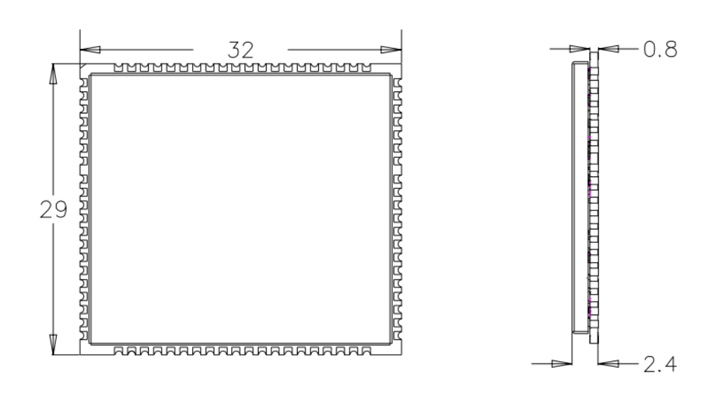
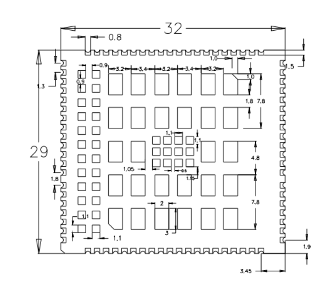
The tolerances for dimensions of length and width, height, and PCB thickness are ±0.35 mm, ±0.15 mm, and ±0.1 mm respectively.
SMT package
Stencil opening design
- Stencil thickness: The stencil thickness of the area for the module should be partly stepped up to 0.18 mm–0.2 mm.
- LCC pins: The stencil openings are shrunk inward by 0.1 mm, and moved outward by 1 mm along the direction of length. Along the width direction, the stencil openings are shrunk inward by 0.16 mm (each side by 0.08 mm) with a length of 1.4 mm (module’s lead length, avoiding solder beads), and are moved outward by 0.2 mm (each side by 0.1 mm) with a length of 2 mm (exposed on the areas outside of the bottom of the module leads to increase tinning).
- LGA pins: The total opening area of the stencil should be 60% of the total. If it exceeds 60%, you can set a pitch of 0.3 mm.
Is this page helpful?
YesFeedbackIs this page helpful?
YesFeedback


